récepteur 406mhz fsk et caf de f1lvt th71101 de chez …
TRANSCRIPT


Modules de réception UHF
des balises de détresse
à l’attention des ADRASEC
L’approvisionnement des platines Wawix est arrivé à son terme, il convient donc de
chercher un autre type de module de réception 406Mhz. Mon choix s’est porté sur une puce de chez
Melexis le TH71101 qui est en tout point identique au composant de chez Microchip rfRxd0420
qui, malheureusement, n’est plus fabriqué, ce composant permet la réception en mode FSK.
Pour dessiner le circuit j’utilise KICAD, mais l’ancienne version
(2013.07.07-BZR4022_win_full_version.exe ), cette version se trouve sur le site de KICAD,
download, windows, lien en bas de la page.
Le schéma ne pose guère de problème, les composants sont des cms, on peut trouver la
puce sur internet « Melexis TH71101 » ou chez « Mouser » ou chez « DIGIKEY » ou ailleurs,
chacun fera son choix, je préconise de se grouper afin d’avoir un prix d’achat pas trop élevé, pour
ma part, je l’ai acheté chez « DIGIKEY » mais les frais de douane sont élevés.
Je peux vous faire parvenir le dossier zippé pour Kicad,
Quelques infos sur cette réalisation, j’ai rajouté au schéma d’origine le montage de
Jean-Paul F1LVT sur la recherche automatique de l’émission de la balise, ainsi que la possibilité de
tester la variation de fréquence manuellement. La diode varicap est de récupération, la plage de
fonctionnement est de 17pF à 27pf, à laquelle on rajoute une capa de 8 à 10pf afin d’obtenir une
variation de 35pf à 25pf, le quartz est taillé à 24,70825Mhz, soit une fréquence centrale de 406,032,
ce qui doit permettre de balayer une bande de 406,025Mhz à 406,040Mhz. Pour tester la valeur de
la varicap, je joins le schéma du montage test.
En ce qui concerne le discriminateur 10,7Mhz, j’ai prévu deux type d’emplacement,
soit un CMS (empreinte = SM2010), soit un composant ordinaire, auquel il faudra rajouter un
condensateur de 10 à 12pf en // sur le discri comme prévu sur le plan.
Cordiales 73
F5LEB, Denis


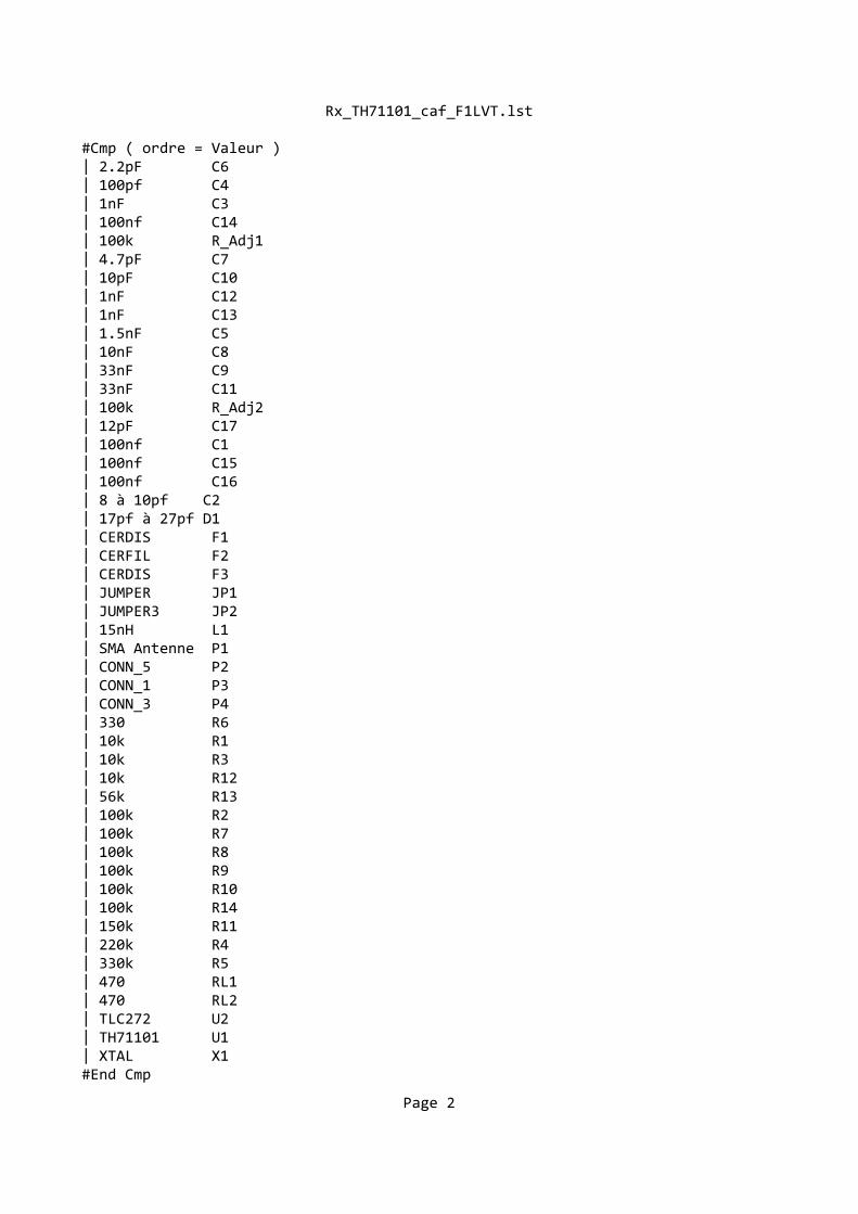
Rx_TH71101_caf_F1LVT.lsteeschema (2013-07-07 BZR 4022)-stable >> Creation date: 30/07/2018 20:44:57#Cmp ( ordre = Référence )| C1 100nf | C2 8 à 10pf | C3 1nF | C4 100pf | C5 1.5nF | C6 2.2pF | C7 4.7pF | C8 10nF | C9 33nF | C10 10pF | C11 33nF | C12 1nF | C13 1nF | C14 100nf | C15 100nf | C16 100nf | C17 12pF | D1 17pf à 27pf| F1 CERDIS | F2 CERFIL | F3 CERDIS | JP1 JUMPER | JP2 JUMPER3 | L1 15nH | P1 SMA Antenne | P2 CONN_5 | P3 CONN_1 | P4 CONN_3 | R1 10k | R2 100k | R3 10k | R4 220k | R5 330k | R6 330 | R7 100k | R8 100k | R9 100k | R10 100k | R11 150k | R12 10k | R13 56k | R14 100k | R_Adj1 100k | R_Adj2 100k | RL1 470 | RL2 470 | U1 TH71101 | U2 TLC272 | X1 XTAL #End Cmp
Page 1
Rx_TH71101_caf_F1LVT.lst
#Cmp ( ordre = Valeur )| 2.2pF C6 | 100pf C4 | 1nF C3 | 100nf C14 | 100k R_Adj1 | 4.7pF C7 | 10pF C10 | 1nF C12 | 1nF C13 | 1.5nF C5 | 10nF C8 | 33nF C9 | 33nF C11 | 100k R_Adj2 | 12pF C17 | 100nf C1 | 100nf C15 | 100nf C16 | 8 à 10pf C2 | 17pf à 27pf D1 | CERDIS F1 | CERFIL F2 | CERDIS F3 | JUMPER JP1 | JUMPER3 JP2 | 15nH L1 | SMA Antenne P1 | CONN_5 P2 | CONN_1 P3 | CONN_3 P4 | 330 R6 | 10k R1 | 10k R3 | 10k R12 | 56k R13 | 100k R2 | 100k R7 | 100k R8 | 100k R9 | 100k R10 | 100k R14 | 150k R11 | 220k R4 | 330k R5 | 470 RL1 | 470 RL2 | TLC272 U2 | TH71101 U1 | XTAL X1 #End Cmp
Page 2

Rx_TH71101_caf_F1LVT.lst
#End List
Page 3
TH71101 315/433MHz
FSK/ASK Receiver
39010 71101 Page 1 of 21 Data Sheet Rev. 018 Jun/13
Features Single-conversion superhet architecture for low external component count FSK demodulation with phase-coincidence demodulator Low current consumption in active mode and very low standby current Switchable LNA gain for improved dynamic range RSSI allows signal strength indication and ASK detection 32-pin Low profile Quad Flat Package (LQFP)
Ordering Code Product Code Temperature Code Package Code Option Code Packing Form Code TH71101 E NE CAA-000 RE TH71101 E NE CAA-000 TR
-40°C to 85°C
!""#"$%%$###$
Application Examples General digital data transmission Tire Pressure Monitoring Systems (TPMS) Remote Keyless Entry (RKE) Wireless access control Alarm and security systems Garage door openers Remote Controls Home and building automation Low-power telemetry systems
Pin Description
General Description The TH71101 FSK/ASK single-conversion superheterodyne receiver IC is designed for applications in the European 433MHz industrial-scientific-medical (ISM) band, according to the EN 300 220 telecommunications standard. It can also be used for any other system with carrier frequencies ranging from 300MHz to 450MHz (e.g. for applications according to FCC part 15 and ARIB STD-T67).
VE
E_LN
AC
OU
T_LN
A
IN_
MIX
1
VE
E_M
IX
IF_1P
IF_1N
VC
C_
MIX
GA
IN_L
NA
VC
C_B
IAS
VE
E_B
IAS
OA
P
OA
NO
UT
_O
A
RS
SI
OU
TP
VEE_RO
RO
ENRX
VEE_LNA
IN_LNA
VCC_LNA
LF
VCC_PLL
OUT_IFA
FBC1
FBC2
IN_IFA
VEE_IF
OUT_MIX2
VCC_IF
1
32
8
9
2425
1716

TH71101 315/433MHz
FSK/ASK Receiver
39010 71101 Page 2 of 21 Data Sheet Rev. 018 Jun/13
Document Content
1 Theory of Operation ...................................................................................................3
1.1 General .............................................................................................................................. 3
1.2 Technical Data Overview ................................................................................................... 3
1.3 Block Diagram.................................................................................................................... 4
1.4 Mode Configurations .......................................................................................................... 4
1.5 LNA GAIN Control.............................................................................................................. 4
1.6 Frequency Planning ........................................................................................................... 4
1.6.1 Selected Frequency Plans ........................................................................................................... 5
1.6.2 Maximum Frequency Coverage................................................................................................... 5
2 Pin Definitions and Descriptions ..............................................................................6
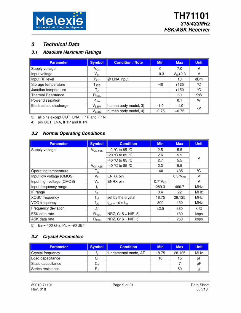
3 Technical Data............................................................................................................9
3.1 Absolute Maximum Ratings................................................................................................ 9
3.2 Normal Operating Conditions ............................................................................................. 9
3.3 Crystal Parameters ............................................................................................................ 9
3.4 DC Characteristics ........................................................................................................... 10
3.5 AC System Characteristics............................................................................................... 11
4 Test Circuits .............................................................................................................12
4.1 Standard FSK Reception.................................................................................................. 12
4.1.1 Standard FSK Application Circuit............................................................................................... 12
4.1.2 Standard FSK Component List .................................................................................................. 13
4.2 Narrow Band FSK Reception ........................................................................................... 14
4.2.1 Narrow Band FSK Application Circuit ........................................................................................ 14
4.2.2 Narrow Band FSK Component List............................................................................................ 15
4.3 ASK Reception................................................................................................................. 16
4.3.1 ASK Application Circuit .............................................................................................................. 16
4.3.2 ASK Component List.................................................................................................................. 17
5 Package Description................................................................................................18
5.1 Soldering Information ....................................................................................................... 18
6 Standard information regarding manufacturability of Melexis products with different soldering processes .................................................................................19
7 ESD Precautions ......................................................................................................19
8 Disclaimer .................................................................................................................20

TH71101 315/433MHz
FSK/ASK Receiver
39010 71101 Page 3 of 21 Data Sheet Rev. 018 Jun/13
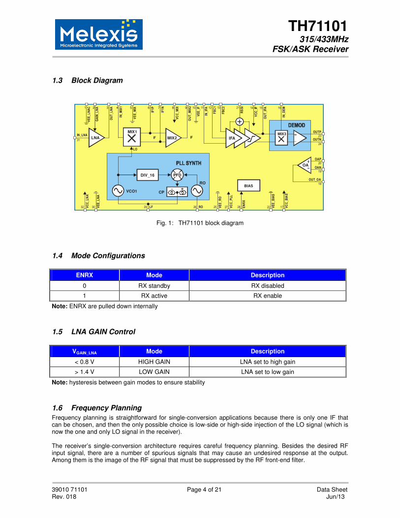
1 Theory of Operation
1.1 General
With the TH71101 receiver chip, various circuit configurations can be arranged in order to meet a number of different customer requirements. For FSK reception the IF tank used in the phase coincidence demodulator can be constituted by an external ceramic discriminator. In ASK configuration, the RSSI signal is fed to an ASK detector, which is constituted by the operational amplifier. A double-conversion variant, called TH71102, is also available. This receiver IC allows a higher degree of image rejection, achieved in conjunction with an RF front-end filter. Both RXICs have the same die. At the TH71102, the second mixer (MIX2) is used to down-convert the first IF (IF1) to the second IF (IF2). At the TH71101, MIX2 operates as an amplifier. Efficient RF front-end filtering is realized by using a SAW, ceramic or helix filter in front of the LNA and by adding an LC filter at the LNA output. The TH71101 receiver IC consists of the following building blocks: PLL synthesizer (PLL SYNTH) for generation of the local oscillator signal LO, parts of the PLL SYNTH
are: the high-frequency VCO1, the feedback divider DIV_16, a phase-frequency detector (PFD) with charge pump (CP) and a crystal-based reference oscillator (RO)
Low-noise amplifier (LNA) for high-sensitivity RF signal reception First mixer (MIX1) for down-conversion of the RF signal to the IF IF pre amplifier which is a mixer cell (MIX2) that operates as an amplifier IF amplifier (IFA) to amplify and limit the IF signal and for RSSI generation Phase coincidence demodulator (DEMOD) with third mixer (MIX3) to demodulate the IF signal Operational amplifier (OA) for data slicing, filtering and ASK detection Bias circuitry for bandgap biasing and circuit shutdown
1.2 Technical Data Overview
Input frequency range: 300to 450 MHz Power supply range: 2.3 to 5.5 V @ ASK Temperature range: -40 to +85 °C Standby current: 50 nA Operating current: 6.5 mA @ low gain 8.2 mA @ high gain Sensitivity: -113 dBm @ ASK 1) -107 dBm @ FSK 2) Maximum data rate: 260 kbps NRZ @ ASK 180 kbps NRZ @ FSK
Range of IF: 400 kHz to 22 MHz Maximum input level: -10 dBm @ ASK 0 dBm @ FSK Image rejection: > 45 dB (e.g. with 433.92
MHz SAW front-end filter and at 10.7 MHz IF) Spurious emission: < -70 dBm
Input frequency acceptance range: up to ±100 kHz RSSI range: 70 dB
FSK deviation range: ±2.5 kHz to ±80 kHz
1) at 4 kbps NRZ, BER = 3⋅10-3
, 180 kHz IF filter BW, without SAW front-end-filter loss
2) at 4 kbps NRZ, BER = 3⋅10-3
, ± 20 kHz FSK deviation, 180 kHz IF filter BW, without SAW front-end-filter loss
TH71101 315/433MHz
FSK/ASK Receiver
39010 71101 Page 4 of 21 Data Sheet Rev. 018 Jun/13
1.3 Block Diagram
Fig. 1: TH71101 block diagram
1.4 Mode Configurations
ENRX Mode Description
0 RX standby RX disabled
1 RX active RX enable
Note: ENRX are pulled down internally
1.5 LNA GAIN Control
VGAIN_LNA Mode Description
< 0.8 V HIGH GAIN LNA set to high gain
> 1.4 V LOW GAIN LNA set to low gain
Note: hysteresis between gain modes to ensure stability
1.6 Frequency Planning
Frequency planning is straightforward for single-conversion applications because there is only one IF that can be chosen, and then the only possible choice is low-side or high-side injection of the LO signal (which is now the one and only LO signal in the receiver). The receiver’s single-conversion architecture requires careful frequency planning. Besides the desired RF input signal, there are a number of spurious signals that may cause an undesired response at the output. Among them is the image of the RF signal that must be suppressed by the RF front-end filter.
MIX1
4
8
5
6 7
9
BIAS
VCO1
PFD
RO
CP
OA
LNA
32
MIX2
MIX3
IFA
DIV_16

TH71101 315/433MHz
FSK/ASK Receiver
39010 71101 Page 5 of 21 Data Sheet Rev. 018 Jun/13
By using the internal PLL synthesizer of the TH71101 with the fixed feedback divider ratio of N = 16 (DIV_16), two types of down-conversion are possible: low-side injection of LO and high-side injection of LO. The following table summarizes some equations that are useful to calculate the crystal reference frequency (REF) and the LO frequency, for a given RF and IF.
Injection type low high
REF (RF – IF)/16 (RF + IF)/16
LO 16 • REF 16 • REF
IF RF – LO LO – RF
RF image RF – 2IF RF + 2IF
1.6.1 Selected Frequency Plans
The following table depicts crystal, LO and image signals considering the examples of 315 MHz and 433.92 MHz RF reception at IF = 10.7 MHz.
Signal type RF = 315 MHz RF = 315 MHz RF = 433.92 MHz RF = 433.92 MHz
Injection type low high low high
REF / MHz 19.01875 20.35625 26.45125 27.78875
LO / MHz 304.3 325.7 423.22 444.62
RF image / MHz 293.6 336.4 412.52 455.32
The selection of the reference crystal frequency is based on some assumptions. As for example: the image frequency should not be in a radio band where strong interfering signals might occur (because they could represent parasitic receiving signals), the LO signal should be in the range of 300 MHz to 450 MHz (because this is the optimum frequency range of the VCO1). Furthermore the IF should be as high as possible to achieve highest RF image rejection. The columns in bold depict the selected frequency plans to receive at 315 MHz and 433.92 MHz, respectively.
1.6.2 Maximum Frequency Coverage
Parameter fmin fmax
Injection type high low
RF / MHz 289.3 460.7
REF / MHz 18.75 28.125
LO / MHz 300 450
IF/ MHz 10.7 10.7
TH71101 315/433MHz
FSK/ASK Receiver
39010 71101 Page 6 of 21 Data Sheet Rev. 018 Jun/13
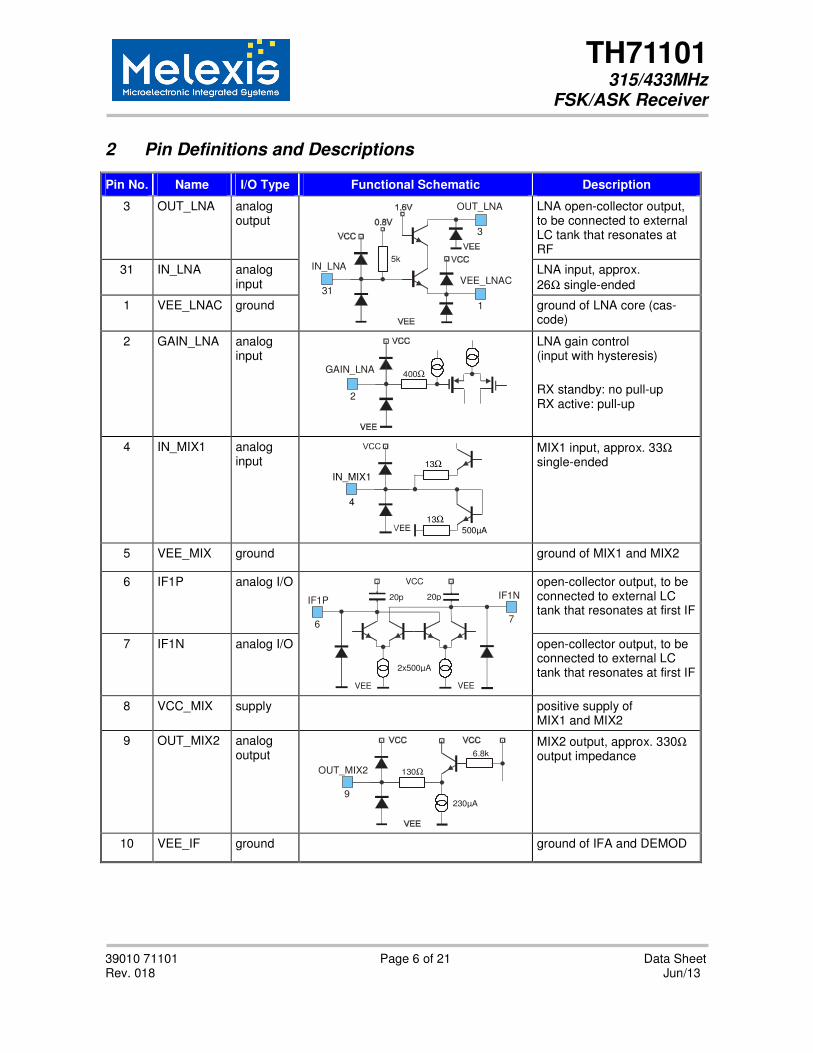
2 Pin Definitions and Descriptions
Pin No. Name I/O Type Functional Schematic Description
3 OUT_LNA analog output
LNA open-collector output, to be connected to external LC tank that resonates at RF
31 IN_LNA analog input
LNA input, approx.
26Ω single-ended
1 VEE_LNAC ground
OUT_LNA
3
5k
VEE_LNAC
1
IN_LNA
31
ground of LNA core (cas-code)
2 GAIN_LNA analog input
GAIN_LNA
2
400Ω
LNA gain control (input with hysteresis)
RX standby: no pull-up RX active: pull-up
4 IN_MIX1 analog input
IN_MIX1
4
500µA
13Ω
13Ω
MIX1 input, approx. 33Ω single-ended
5 VEE_MIX ground ground of MIX1 and MIX2
6 IF1P analog I/O open-collector output, to be connected to external LC tank that resonates at first IF
7 IF1N analog I/O
20p20p
2x500µA
IF1P
6
VEE
VCC
VEE
IF1N
7
open-collector output, to be connected to external LC tank that resonates at first IF
8 VCC_MIX supply positive supply of MIX1 and MIX2
9 OUT_MIX2 analog output
130Ω
6.8k
OUT_MIX2
9230µA
MIX2 output, approx. 330Ω output impedance
10 VEE_IF ground ground of IFA and DEMOD

TH71101 315/433MHz
FSK/ASK Receiver
39010 71101 Page 7 of 21 Data Sheet Rev. 018 Jun/13
Pin No. Name I/O Type Functional Schematic Description
11 IN_IFA analog input
IFA input, approx. 2.2kΩ input impedance
12 FBC1 analog I/O to be connected to external IFA feedback capacitor
13 FBC2 analog I/O
2.2k 2.2k
200µA
IN_IFA
11
VEE
VEE
VCC
VEE
VCC
12
FBC1
FBC2
13
VEE
VCC
to be connected to external IFA feedback capacitor
14 VCC_IF supply positive supply of IFA and DEMOD
15 OUT_IFA analog I/O
OUT_IFA
1540µA
IFA output and MIX3 input (of DEMOD)
16 IN_DEM analog input
IN_DEM
16
47k
DEMOD input, to MIX3 core
17 VCC_BIAS supply positive supply of general bias system and OA
18 OUT_OA analog output
OUT_OA
18
50Ω
OA output, 40uA current drive capability
19 OAN analog input
negative OA input
20 OAP analog input
20µA
19
OAN 50Ω
20
OAP50Ω
positive OA input

TH71101 315/433MHz
FSK/ASK Receiver
39010 71101 Page 8 of 21 Data Sheet Rev. 018 Jun/13
Pin No. Name I/O Type Functional Schematic Description
21 RSSI analog output
I (Pi)RSSI
21
50Ω
36k
RSSI output, for RSSI and ASK detection, approx.
36kΩ output impedance
22 VEE_BIAS ground ground of general bias system and OA
23 OUTP analog output
FSK positive output, output
impedance of 100kΩ to
300kΩ
24 OUTN analog output
OUTPOUTN
2324
50Ω
20µA 20µA
FSK negative output, output
impedance of 100kΩ to
300kΩ
25 VEE_RO ground ground of DIV, PFD, RO and charge pump
26 RO analog input
RO
26
30p
30p
50k
RO input, Colpitts type oscillator with internal feed-back capacitors
27 VCC_PLL supply positive supply of DIV, PFD, RO and charge pump
28 ENRX digital input
ENRX
28
1.5k
mode control input, CMOS-compatible with internal pull-down circuit
29 LF analog I/O
LF
29
200Ω
400Ω
4p
charge pump output and VCO1 control input
30 VEE_LNA ground ground of LNA biasing
32 VCC_LNA supply positive supply of LNA biasing
TH71101 315/433MHz
FSK/ASK Receiver
39010 71101 Page 9 of 21 Data Sheet Rev. 018 Jun/13
3 Technical Data
3.1 Absolute Maximum Ratings
Parameter Symbol Condition / Note Min Max Unit
Supply voltage VCC 0 7.0 V
Input voltage VIN - 0.3 Vcc+0.3 V
Input RF level PiRF @ LNA input 10 dBm
Storage temperature TSTG -40 +125 °C
Junction temperature TJ +150 °C
Thermal Resistance RthJA 60 K/W
Power dissipation Pdiss 0.1 W
VESD1 human body model, 3) -1.0 +1.0 Electrostatic discharge
VESD2 human body model, 4) -0.75 +0.75 kV
3) all pins except OUT_LNA, IF1P and IF1N
4) pin OUT_LNA, IF1P and IF1N
3.2 Normal Operating Conditions
Parameter Symbol Condition Min Max Unit
0 °C to 85 °C 2.5 5.5
-20 °C to 85 °C 2.6 5.5
VCC, FSK
-40 °C to 85 °C 2.7 5.5
Supply voltage
VCC, ASK -40 °C to 85 °C 2.3 5.5
V
Operating temperature TA -40 +85 ºC
Input low voltage (CMOS) VIL ENRX pin 0.3*VCC V
Input high voltage (CMOS) VIH ENRX pin 0.7*VCC V
Input frequency range fi 289.3 460.7 MHz
IF range fIF 0.4 22 MHz
XOSC frequency fref set by the crystal 18.75 28.125 MHz
VCO frequency fLO fLO = 16 • fref 300 450 MHz
Frequency deviation ∆f ±2.5 ±80 kHz
FSK data rate RFSK NRZ, C15 = NIP, 5) 180 kbps
ASK data rate RASK NRZ, C16 = NIP, 5) 260 kbps
5) BIF = 400 kHz, PIN = -90 dBm
3.3 Crystal Parameters
Parameter Symbol Condition Min Max Unit
Crystal frequency f0 fundamental mode, AT 18.75 28.125 MHz
Load capacitance CL 10 15 pF
Static capacitance C0 7 pF
Series resistance R1 50 Ω

TH71101 315/433MHz
FSK/ASK Receiver
39010 71101 Page 10 of 21 Data Sheet Rev. 018 Jun/13
3.4 DC Characteristics
all parameters under normal operating conditions, unless otherwise stated; typical values at TA= 23 °C and VCC = 3 V
Parameter Symbol Condition Min Typ Max Unit
Operating Currents
Standby current ISBY ENRX=0 50 100 nA
Supply current at low gain ICC, low ENRX=1 GAIN_LNA=1
4.0 6.5 12.0 mA
Supply current at high gain ICC, high ENRX=1 GAIN_LNA=0
4.5 8.2 14.0 mA
Digital Pin Characteristics
Input low voltage CMOS VIL ENRX pin -0.3 0.3*Vcc V
Input high voltage CMOS VIH ENRX pin 0.7*VCC VCC+0.3 V
Pull down current ENRX pin
IPDEN ENRX=1 0.1 2 10 µA
Low level input current ENRX pin
IINLEN ENRX=0 0.05 µA
Analog Pin Characteristics
High level input current GAIN_LNA pin
IINHGAIN GAIN_LNA=1 0.05 µA
Pull up current GAIN_LNA pin active
IPUGAINa GAIN_LNA=0
ENRX=1
0.08 0.15 0.3 µA
Pull up current GAIN_LNA pin standby
IPUGAINs GAIN_LNA=0
ENRX=0
0.05 µA
High gain input voltage VIHGAIN ENRX=1 0.7 V
Low gain input voltage VILGAIN ENRX=1 1.5 V
Opamp Characteristics
Opamp input offset voltage Voffs -35 35 mV
Opamp input offset current Ioffs IOAP – IOAN -50 50 nA
Opamp input bias current Ibias 0.5 * (IOAP + IOAN) -150 150 nA
RSSI Characteristics
RSSI voltage at low input level VRSSI, low Pi = -65 dBm, GAIN_LNA=1
0.5 1.0 1.5 V
RSSI voltage at high input level VRSSI, high Pi = -35 dBm, GAIN_LNA=1
1.2 1.9 2.5 V

TH71101 315/433MHz
FSK/ASK Receiver
39010 71101 Page 11 of 21 Data Sheet Rev. 018 Jun/13
3.5 AC System Characteristics
all parameters under normal operating conditions, unless otherwise stated; typical values at TA = 23 °C and VCC = 3 V, RF at 433.92 MHz; SAW frond-end filter loss and IF at 10.7 MHz; all parameters based on test circuits as shown in Fig. 2, Fig.3 and Fig. 5
Parameter Symbol Condition Min Typ Max Unit
Receive Characteristics
Input sensitivity – FSK (standard)
Pmin, ST BIF = 180kHz,
∆f = ±20kHz, 4kbps NRZ,
BER ≤ 3⋅10-3
, 6)
-104 dBm
Input sensitivity – FSK (narrow band)
Pmin, NB BIF = 30kHz,
∆f = ±5kHz, 4kbps NRZ,
BER ≤ 3⋅10-3
, 6)
-108 dBm
Input sensitivity – ASK Pmin, ASK BIF = 180kHz, 4kbps NRZ,
BER ≤ 3⋅10-3
, 6)
-110 dBm
Maximum input signal – FSK Pmax, FSK BER ≤ 3⋅10-3
GAIN_LNA = 1
0 dBm
Maximum input signal – ASK Pmax, ASK BER ≤ 3⋅10-3
GAIN_LNA = 1
-10 dBm
Spurious emission Pspur -70 dBm
Image rejection ∆Pimag 45 dB
Start-up Parameters
Crystal start-up time TXTL ENRX from 0 to 1 0.9 ms
Receiver start-up time TRX ENRX from 0 to 1,
depends on data slicer time constant, valid data at output
TXTL
+
R4 · C17
PLL Parameters
VCO gain KVCO 250 MHz/V
Charge pump current ICP 60 µA
6) incl. 3 dB loss of front-end SAW filter
TH71101 315/433MHz
FSK/ASK Receiver
39010 71101 Page 12 of 21 Data Sheet Rev. 018 Jun/13
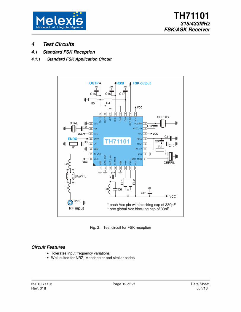
4 Test Circuits
4.1 Standard FSK Reception
4.1.1 Standard FSK Application Circuit
Fig. 2: Test circuit for FSK reception
Circuit Features
• Tolerates input frequency variations
• Well-suited for NRZ, Manchester and similar codes
CERFIL
OU
TP
VE
E
OU
T_
LN
A
IN_
MIX
1
VE
E
IF1
P
IF1
N
VC
C
GA
IN_
LN
A
VEE
OUT_MIX2
IN_IFA
FBC1
FBC2
VCC
OUT_IFA
LF
VEE
IN_LNA
VCC
VEE
ENRX
VCCV
CC
VE
E
OA
P
OA
N
OU
T_
OA
RS
SI
32
31
30
29
28
27
26
25
17
18
19
20
21
22
23
24
9
10
11
12
13
14
15
16
81 2 3 4 5 6 7
ROC12
CERDIS
XTAL
C11
C10
C9
CB*VCC
C16C15
R4R5
C1
C3
R1
RL
2
RL
1
C7
L3 C6
C17
R2
TH71101ENRX
FSK outputRSSIOUTP
* each Vcc pin with blocking cap of 330pF* one global Vcc blocking cap of 33nF
L2
L1
RF input
50
SAWFIL46
1 3

TH71101 315/433MHz
FSK/ASK Receiver
39010 71101 Page 13 of 21 Data Sheet Rev. 018 Jun/13
4.1.2 Standard FSK Component List
Part Size Value
@ 433.92 MHz Tolerance Description
C1 0805 27 pF ±5% crystal series capacitor
C3 0603 1 nF ±10% loop filter capacitor
C6 0603 4.7 pF ±5% LNA output tank capacitor
C7 0603 2.2 pF ±5% MIX1 input matching capacitor
C9 0603 33 nF ±10% IFA feedback capacitor
C10 0603 1 nF ±10% IFA feedback capacitor
C11 0603 1 nF ±10% IFA feedback capacitor
C12 0805 10 pF ±5% DEMOD phase-shift capacitor
C15 0805 100 pF ±5% demodulator output low-pass capacitor, this value for data rates < 20 kbps NRZ
C16 0805 1.5 nF ±10% RSSI output low-pass capacitor
C17 0805 10 nF ±10% data slicer capacitor, this value for data rates > 0.8 kbps NRZ
R1 0603 10 kΩ ±5% loop filter resistor
R2 0603 330 Ω ±5% optional CERFIL output matching resistor
R4 0805 330 kΩ ±5% data slicer resistor
R5 0805 220 kΩ ±5% loading resistor
RL1 0805 470 Ω ±5% MIX1 bias resistor
RL2 0805 470 Ω ±5% MIX1 bias resistor
L1 0603 68 nH ±5%
L2 0603 82 nH ±5%
SAW filter matching inductor from Würth-Elektronik (WE-KI series), or equivalent part
L3 0603 15 nH ±5% LNA output tank inductor from Würth-Elektronik (WE-KI series), or equivalent part
XTAL SMD 6x3.5
26.45125 MHz @ RF = 433.92 MHz
±25ppm cal.
±30ppm temp.
fundamental-mode crystal from Telcona/Horizon or equivalent part
SAWFIL SMD 3x3
SAFCC433MBL0X00 (f0 = 433.92 MHz)
B3dB = 840 kHz low-loss SAW filter from Murata, or equivalent part
CERFIL SMD 3.45x3.1
SFECF10M7HA00 B3dB = 180 kHz ceramic filter from Murata, or equivalent part
CERDIS SMD 4.5x2
CDSCB10M7GA135 ceramic discriminator from Murata, or equivalent part
• For component values for other frequencies, please refer to the EVB descriptions
TH71101 315/433MHz
FSK/ASK Receiver
39010 71101 Page 14 of 21 Data Sheet Rev. 018 Jun/13
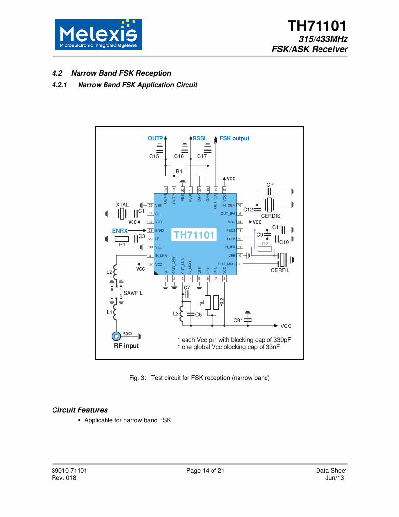
4.2 Narrow Band FSK Reception
4.2.1 Narrow Band FSK Application Circuit
Fig. 3: Test circuit for FSK reception (narrow band)
Circuit Features
• Applicable for narrow band FSK
CERFIL
OU
TP
VE
E
OU
T_
LN
A
IN_
MIX
1
VE
E
IF1
P
IF1
N
VC
C
GA
IN_
LN
A
VEE
OUT_MIX2
IN_IFA
FBC1
FBC2
VCC
OUT_IFA
LF
VEE
IN_LNA
VCC
VEE
ENRX
VCCV
CC
VE
E
OA
P
OA
N
OU
T_
OA
RS
SI
32
31
30
29
28
27
26
25
17
18
19
20
21
22
23
24
9
10
11
12
13
14
15
16
81 2 3 4 5 6 7
ROC12
XTAL
C11
C10
C9
CB*VCC
C16C15
R4
C1
C3
R1
RL
2
RL
1
C7
L3 C6
C17
R2
TH71101ENRX
FSK outputRSSIOUTP
* each Vcc pin with blocking cap of 330pF* one global Vcc blocking cap of 33nF
CP
CERDIS
L2
L1
RF input
50
SAWFIL46
1 3

TH71101 315/433MHz
FSK/ASK Receiver
39010 71101 Page 15 of 21 Data Sheet Rev. 018 Jun/13
4.2.2 Narrow Band FSK Component List
Part Size Value
@ 433.92 MHz Tolerance Description
C1 0805 27 pF ±5% crystal series capacitor
C3 0603 1 nF ±10% loop filter capacitor
C6 0603 4.7 pF ±5% LNA output tank capacitor
C7 0603 2.2 pF ±5% MIX1 input matching capacitor
C9 0603 33 nF ±10% IFA feedback capacitor
C10 0603 1 nF ±10% IFA feedback capacitor
C11 0603 1 nF ±10% IFA feedback capacitor
C12 0805 1.5 pF ±5% DEMOD phase-shift capacitor
C15 0805 220 pF ±5% demodulator output low-pass capacitor, this value for data rates < 10 kbps NRZ
C16 0805 1.5 nF ±10% RSSI output low-pass capacitor
C17 0805 10 nF ±10% data slicer capacitor, this value for data rates > 0.8 kbps NRZ
CP 0603 6.8 - 8.2 pF ±5% ceramic resonator loading capacitor
R1 0603 10 kΩ ±5% loop filter resistor
R2 0603 330 Ω ±5% optional CERFIL output matching resistor
R4 0805 330 kΩ ±5% data slicer resistor
RL1 0805 470 Ω ±5% MIX1 bias resistor
RL2 0805 470 Ω ±5% MIX1 bias resistor
L1 0603 68 nH ±5%
L2 0603 82 nH ±5%
SAW filter matching inductor from Würth-Elektronik (WE-KI series), or equivalent part
L3 0603 15 nH ±5% LNA output tank inductor from Würth-Elektronik (WE-KI series), or equivalent part
XTAL SMD 6x3.5
26.45125 MHz @ RF = 433.92 MHz
±25ppm cal.
±30ppm temp.
fundamental-mode crystal from Telcona/Horizon or equivalent part
SAWFIL SMD 3x3
SAFCC433MBL0X00 (f0 = 433.92 MHz)
B3dB = 840 kHz low-loss SAW filter from Murata, or equivalent part
SFKLA10M7NL00 B3dB = 30 kHz ceramic filter from Murata, or equivalent part CERFIL
Leaded type SFVLA10M7LF00 B3dB = 80 kHz optional, ceramic filter from Murata, or equivalent part
CERDIS SMD 4.5x2
CDSCB10M7GA135 ceramic discriminator from Murata, or equivalent part
• For component values for other frequencies, please refer to the EVB descriptions

TH71101 315/433MHz
FSK/ASK Receiver
39010 71101 Page 16 of 21 Data Sheet Rev. 018 Jun/13
4.3 ASK Reception
4.3.1 ASK Application Circuit
Fig. 5: Test circuit for ASK reception
CERFIL
OU
TP
VE
E
OU
T_
LN
A
IN_
MIX
1
VE
E
IF1
P
IF1
N
VC
C
GA
IN_
LN
A
VEE
OUT_MIX2
IN_IFA
FBC1
FBC2
VCC
OUT_IFA
LF
VEE
IN_LNA
VCC
VEE
ENRX
VCC
VC
C
VE
E
OA
P
OA
N
OU
T_
OA
RS
SI
32
31
30
29
28
27
26
25
17
18
19
20
21
22
23
24
9
10
11
12
13
14
15
16
81 2 3 4 5 6 7
RO
XTAL
C11
C10
C9
CB*VCC
C16
R4
C1
C3
R1
RL
2
RL
1
C7
L3 C6
C17
R2
TH71101ENRX
ASK outputRSSI
* each Vcc pin with blocking cap of 330pF* one global Vcc blocking cap of 33nF
L2
L1
RF input
50
SAWFIL46
1 3
TH71101 315/433MHz
FSK/ASK Receiver
39010 71101 Page 17 of 21 Data Sheet Rev. 018 Jun/13
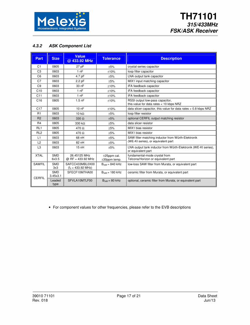
4.3.2 ASK Component List
Part Size Value
@ 433.92 MHz Tolerance Description
C1 0805 27 pF ±5% crystal series capacitor
C3 0603 1 nF ±10% loop filter capacitor
C6 0603 4.7 pF ±5% LNA output tank capacitor
C7 0603 2.2 pF ±5% MIX1 input matching capacitor
C9 0603 33 nF ±10% IFA feedback capacitor
C10 0603 1 nF ±10% IFA feedback capacitor
C11 0603 1 nF ±10% IFA feedback capacitor
C16 0805 1.5 nF ±10% RSSI output low-pass capacitor, this value for data rates < 10 kbps NRZ
C17 0805 10 nF ±10% data slicer capacitor, this value for data rates > 0.8 kbps NRZ
R1 0603 10 kΩ ±5% loop filter resistor
R2 0603 330 Ω ±5% optional CERFIL output matching resistor
R4 0805 330 kΩ ±5% data slicer resistor
RL1 0805 470 Ω ±5% MIX1 bias resistor
RL2 0805 470 Ω ±5% MIX1 bias resistor
L1 0603 68 nH ±5%
L2 0603 82 nH ±5%
SAW filter matching inductor from Würth-Elektronik (WE-KI series), or equivalent part
L3 0603 15 nH ±5% LNA output tank inductor from Würth-Elektronik (WE-KI series), or equivalent part
XTAL SMD 6x3.5
26.45125 MHz @ RF = 433.92 MHz
±25ppm cal.
±30ppm temp.
fundamental-mode crystal from Telcona/Horizon or equivalent part
SAWFIL SMD 3x3
SAFCC433MBL0X00 (f0 = 433.92 MHz)
B3dB = 840 kHz low-loss SAW filter from Murata, or equivalent part
SMD 3.45x3.1
SFECF10M7HA00 B3dB = 180 kHz ceramic filter from Murata, or equivalent part
CERFIL Leaded
type SFVLA10M7LF00 B3dB = 80 kHz optional, ceramic filter from Murata, or equivalent part
• For component values for other frequencies, please refer to the EVB descriptions
TH71101 315/433MHz
FSK/ASK Receiver
39010 71101 Page 18 of 21 Data Sheet Rev. 018 Jun/13
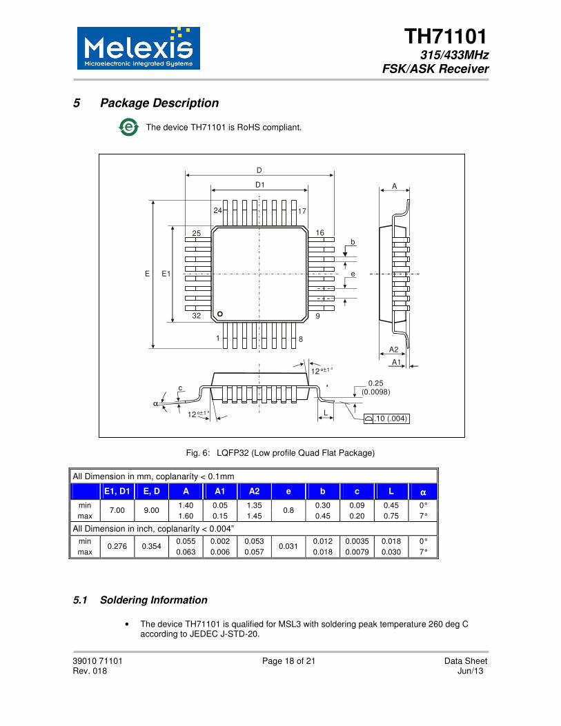
5 Package Description
The device TH71101 is RoHS compliant.
Fig. 6: LQFP32 (Low profile Quad Flat Package)
All Dimension in mm, coplanaríty < 0.1mm
E1, D1 E, D A A1 A2 e b c L αααα
min 1.40 0.05 1.35 0.30 0.09 0.45 0°
max 7.00 9.00
1.60 0.15 1.45 0.8
0.45 0.20 0.75 7°
All Dimension in inch, coplanaríty < 0.004”
min 0.055 0.002 0.053 0.012 0.0035 0.018 0°
max 0.276 0.354
0.063 0.006 0.057 0.031
0.018 0.0079 0.030 7°
5.1 Soldering Information
• The device TH71101 is qualified for MSL3 with soldering peak temperature 260 deg C according to JEDEC J-STD-20.
1
32
25
1724
8
9
16
D
D1
E1 e
b
E
A2
A
A1
L
c0.25
(0.0098)
12° 1°+
12° 1°+
.10 (.004)

TH71101 315/433MHz
FSK/ASK Receiver
39010 71101 Page 19 of 21 Data Sheet Rev. 018 Jun/13
6 Standard information regarding manufacturability of Melexis products with different soldering processes
Our products are classified and qualified regarding soldering technology, solderability and moisture sensitiv-ity level according to following test methods: Reflow Soldering SMD’s (Surface Mount Devices)
• IPC/JEDEC J-STD-020 Moisture/Reflow Sensitivity Classification for Nonhermetic Solid State Surface Mount Devices (classification reflow profiles according to table 5-2)
• EIA/JEDEC JESD22-A113 Preconditioning of Nonhermetic Surface Mount Devices Prior to Reliability Testing (reflow profiles according to table 2)
Wave Soldering SMD’s (Surface Mount Devices) and THD’s (Through Hole Devices)
• EN60749-20 Resistance of plastic- encapsulated SMD’s to combined effect of moisture and soldering heat
• EIA/JEDEC JESD22-B106 and EN60749-15 Resistance to soldering temperature for through-hole mounted devices
Iron Soldering THD’s (Through Hole Devices)
• EN60749-15 Resistance to soldering temperature for through-hole mounted devices
Solderability SMD’s (Surface Mount Devices) and THD’s (Through Hole Devices)
• EIA/JEDEC JESD22-B102 and EN60749-21 Solderability
For all soldering technologies deviating from above mentioned standard conditions (regarding peak tempera-ture, temperature gradient, temperature profile etc) additional classification and qualification tests have to be agreed upon with Melexis. The application of Wave Soldering for SMD’s is allowed only after consulting Melexis regarding assurance of adhesive strength between device and board. Melexis is contributing to global environmental conservation by promoting lead free solutions. For more in-formation on qualifications of RoHS compliant products (RoHS = European directive on the Restriction Of the use of certain Hazardous Substances) please visit the quality page on our website: http://www.melexis.com/quality.aspx
7 ESD Precautions Electronic semiconductor products are sensitive to Electro Static Discharge (ESD). Always observe Electro Static Discharge control procedures whenever handling semiconductor products.

TH71101 315/433MHz
FSK/ASK Receiver
39010 71101 Page 20 of 21 Data Sheet Rev. 018 Jun/13
8 Disclaimer Devices sold by Melexis are covered by the warranty and patent indemnification provisions appearing in its Term of Sale. Melexis makes no warranty, express, statutory, implied, or by description regarding the infor-mation set forth herein or regarding the freedom of the described devices from patent infringement. Melexis reserves the right to change specifications and prices at any time and without notice. Therefore, prior to de-signing this product into a system, it is necessary to check with Melexis for current information. This product is intended for use in normal commercial applications. Applications requiring extended temperature range, unusual environmental requirements, or high reliability applications, such as military, medical life-support or life-sustaining equipment are specifically not recommended without additional processing by Melexis for each application. The information furnished by Melexis is believed to be correct and accurate. However, Melexis shall not be liable to recipient or any third party for any damages, including but not limited to personal injury, property damage, loss of profits, loss of use, interrupt of business or indirect, special incidental or consequential damages, of any kind, in connection with or arising out of the furnishing, performance or use of the technical data herein. No obligation or liability to recipient or any third party shall arise or flow out of Melexis’ rendering of technical or other services. © 2013 Melexis NV. All rights reserved.
For the latest version of this document, go to our website at www.melexis.com
Or for additional information contact Melexis Direct:
Europe, Africa, Asia: America:
Phone: +32 1367 0495 Phone: +1 248 306 5400 E-mail: [email protected] E-mail: [email protected]
ISO/TS 16949 and ISO14001 Certified
