solutions et matériaux nouveaux pour guide d'onde
TRANSCRIPT
UNIVERSITÉ DE SHERBROOKE
Faculté de génie
Département de génie Électrique
Solutions et Matériaux Nouveaux pour Guide d'Onde
Térahertz
Novel Solutions and Materials for Terahertz Wave
Guiding
Thèse de doctorat
Spécialité: génie électrique
Seyed Ali Malek Abadi
Jury: François Boone (directeur)
Serge Charlebois (co-directeur)
Dominic Deslandes (co-directeur)
Denis Morris
Pierre Berini
Daryoosh Saeedkia
Sherbrooke (Québec) Canada Avril 2014

i
To my father, mother and my lovely wife
Sarvenaz
ii
RÉSUMÉ
Dans cette thèse, une étude approfondie sur des matériaux et des solutions pratiques est
réalisée afin de répondre aux difficultés rencontrées dans la propagation des ondes à des
fréquences térahertz (THz). Deux matériaux ont été identifiés comme étant prometteur: le
graphène et le silicium à haute résistivité (HR-Si). Une première solution, basée sur des guides
d’ondes à plaques parallèles (parallel plate waveguide-PPWG) avec des conditions de
fermetures conducteur parfait (perfect electric conductor-PEC) -- graphène et graphène --
graphène a été analysée dans un premier temps. En considérant l'excitation du graphène par un
champ électrique seulement, puis par un champ électromagnétique statique, les équations de
Maxwell ont été résolues sous ces deux conditions et les constantes de propagations des
différents modes ont été extraites. La démonstration de l'existence d'un mode propagatif
hybride à l'intérieur du guide est faite dès que le graphène est excité par un champ magnétique.
De plus, il est montré que l'intensité de chaque type de modes, transverse électrique (TE) ou
transverse magnétique (TM), peut être ajustée suivant les champs d'excitation du graphène.
Bien que le guide à plaques parallèles utilisant du graphène permette d'avoir des propriétés
agiles, soit le contrôle des modes selon l'excitation du graphène, il n'en reste pas moins vrai
que la faible conductivité intrinsèque au graphène conduit à un problème d'atténuation
importante de l'onde. De plus, la difficulté d'obtenir des couches de graphène de taille
adéquate entrave le développement de composants et de circuits fonctionnels, utilisables et à
un coût raisonnable. La thèse porte ensuite sur l’étude du silicium haute résistivité pour guider
des ondes aux fréquences térahertz. Tout d’abord, un guide composé d'une couche de HR-Si,
de section rectangulaire dont la largeur est très grande par rapport à la hauteur, est caractérisé
en utilisant un système de spectroscopie dans le domaine du temps, système permettant
d'obtenir un large spectre de fréquences dans le domaine THz. Par cette caractérisation, les
faibles pertes et la faible dispersion du HR-Si est démontrée. Cependant, il est aussi démontré
que la géométrie du guide n'est pas optimale, conduisant à des pertes par dispersion de l'onde à
l'intérieur du guide au fur et à mesure de sa propagation. Aussi, pour éviter cette dispersion, un
confinement de l'onde est proposé en réduisant la largeur de la couche HR-Si pour la rendre de
l'ordre de la hauteur (confinement en x et y, propagation en z) conduisant ainsi à la réalisation
d'un guide d’ondes diélectrique en ruban (dielectric ribbon waveguide-DRW). Une analyse
approfondie de la propagation d'une telle structure a conduit à concevoir un guide à faibles
pertes d'une part, mais également à propagation monomode sur une large bande de fréquence.
Une méthode de fabrication simple a été développée pour réaliser ce type de guide et un banc
de mesure spécifique a été mis en place pour caractériser ce nouveau guide. Les mesures
réalisées utilisent un analyseur de réseaux vectoriel (un PNA-X d'Agilent) auquel est branché
deux têtes de mesure de la compagnie Virginia Diode Inc's (VDI) pour obtenir les bandes de
fréquences désirées. Les sorties sont alors en guide rectangulaire standard, soit WR-8, soit
WR-5 selon la plage de fréquence visée. Les résultats des mesures se comparent très bien avec
les simulations réalisées avec un logiciel utilisant la méthode des éléments finis en trois
dimensions (HFSS de la compagnie ANSYS) permettant d'obtenir les paramètres de la matrice
de diffraction (S) mesurée par l'analyseur de réseau vectoriel. Finalement, dans le chapitre 6,
un filtre passe-bande est développé comme preuve de concept pour l'utilisation du guide DRW
utilisant le matériau HR-Si. Outre les faibles pertes et la propagation monomode d'un tel guide
DRW, il est aussi montré dans cette thèse la facilité du processus de fabrication, le faible coût

iii
de ce procédé ainsi que la possibilité d'intégration avec d'autres composants passifs et actifs.
Avec toutes ces caractéristiques très intéressantes sur différents plans, le guide DRW en HR-Si
apparaît comme une solution très compétitive pour devenir un standard dans la bande de
fréquence des THz.
Mots clés: graphène, silicium haute résistivité, guide d'onde à base de couche diélectrique,
guide d'onde DRW, filtre passe-bande.
iv
ABSTRACT
In this dissertation, novel materials and solutions are scrutinized to circumvent the guiding
difficulties in terahertz (THz) region. Two materials, graphene and high-resistivity silicon
(HR-silicon), are chosen for our research. Parallel plate waveguide (PPWG) with Perfect
Electric Conductor (PEC)-graphene and graphene-graphene plates are considered as the first
possible solution. Assuming that the graphene layers are biased with an electric field only and
both electric and magnetic fields, the Maxwell’s equations are solved and the propagating
modes are derived. It is shown that a hybrid mode propagates inside the guide while the
graphene layers are biased with magnetic fields. Also, it is proved that the intensity of each
propagating modes (TE and TM) can be tuned by the applied bias fields. Although graphene’s
interesting properties gave the PPWG agile capabilities (altering the guiding wave by the
applied electric and magnetic fields), the attenuation problem still remains due to graphene’s
low conductivity. Moreover, lack of proper size graphene layers hinders the development of
practical high-frequency components/circuits. Chapters 4, 5 and 6 of this dissertation are
dedicated to the study of HR-silicon waveguides. Initially, an HR-silicon slab waveguide is
characterized using THz time domain spectroscopy (THz-TDS) system. The low-loss and low-
dispersive nature of the HR-silicon is proved. However, the waveguide present attenuations
due to wave broadening as it propagates down the slab. To eliminate this attenuation source,
the wave is confined, in both x- and y-directions (assuming propagation toward the z-axis) by
limiting the slab in its infinite direction (so-called dielectric ribbon waveguide – DRW). A
modal analysis of the DRW leads to a design method for low-loss and mono-mode
propagation. A fabrication method is developed for the DRWs and a measurement setup is
proposed. An Agilent PNA-X network analyser with Virginia Diodes Inc.’s (VDI) WR-8 and
WR-5 extension modules is employed to characterize the designed guide. The measurement
results agree very well with simulations performed by finite element method based simulation
software from Ansys (HFSS). Finally, in Chapter 6, bandpass filter design process is
developed based on the DRWs. In addition to low-loss and mono-mode characteristics of the
DRWs, their cheap and straightforward fabrication process and the feasibility of realizing and
integrating with other passive/active components make them an outstanding candidate for the
THz guiding applications.
Key words: graphene, high resistivity silicon, dielectric slab waveguide, dielectric ribbon
waveguide, bandpass filter

v
ACKNOWLEDEGMENTS
First and foremost, I would like to thank my advisors Profs. François Boone, Serge Charlebois
and Dominic Deslandes for not only giving me the opportunity to work on this project but also
for advising me along the way. Your insight, support, and patience have guided me through
difficult periods.
I also would like to thank Prof. Denis Morris for sharing his lab and Dr. Daryoosh Saeedkia
and Prof. Pierre Berini for agreeing to serve on my thesis committee. I also would like to
appreciate all the helps and supports from the staff at 3IT.
Finally, I wish to thank my parents, my wife Sarvenaz, my brothers and my friends for their
unconditional love and support during this journey.
vi
TABLE OF CONTENTS
RÉSUMÉ ................................................................................................................................ ii
ABSTRACT .......................................................................................................................... iv
ACKNOWLEDEGMENTS .................................................................................................... v
TABLE OF CONTENTS ....................................................................................................... vi
LIST OF FIGURES ................................................................................................................ x
LIST OF TABLES ................................................................................................................ xv
1 THE TERAHERTZ GAP: “A PART OF SPECTRUM THAT HAS BEEN LEAST
EXPLORED”.......................................................................................................................... 1
1.1 The THz gap ............................................................................................................ 1
1.2 THz Applications .................................................................................................... 2
1.3 THz generation and detection .................................................................................. 3
1.4 Needs for new materials and solutions ..................................................................... 4
1.5 Thesis outline .......................................................................................................... 5
2 STATE OF THE ART: NOVEL MATERIALS FOR TERAHERTZ WAVEGUIDING .. 6
2.1 THz Wave Guiding Technology .............................................................................. 6
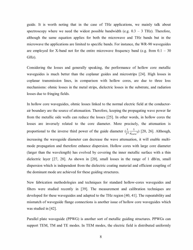
2.1.1 Metallic Waveguides ........................................................................................... 7
2.1.2 Dielectric Waveguides ....................................................................................... 10
2.2 Transparent Guiding Mediums............................................................................... 15
2.2.1 High Resistivity Silicon ..................................................................................... 15
vii
2.2.2 Graphene ........................................................................................................... 17
3 PARALLEL PLATE WAVEGUIDE WITH GRAPHENE PLATES ............................. 19
3.1 Avant-propos ......................................................................................................... 19
3.2 Parallel plate waveguide with anisotropic graphene plates: effect of electric and
magnetic biases ................................................................................................................. 24
3.2.1 Abstract ............................................................................................................. 24
3.2.2 Introduction ....................................................................................................... 24
3.2.3 Graphene Model ................................................................................................ 27
3.2.4 Parallel Plate Waveguide ................................................................................... 30
3.2.5 Conclusion......................................................................................................... 47
4 HIGH-RESISTIVITY SILICON DIELECTRIC SLAB WAVEGUIDE ......................... 48
4.1 Avant-Propos......................................................................................................... 48
4.3 Low-loss low-dispersive high-resistivity silicon dielectric slab waveguide for THz
region 52
4.3.1 Abstract ............................................................................................................. 52
4.3.2 Introduction ....................................................................................................... 52
4.3.3 Theory and Analysis .......................................................................................... 53
4.3.4 Fabrication and Measurement ............................................................................ 54
4.3.5 Conclusion......................................................................................................... 59
5 SILICON DIELECTRIC RIBBON WAVEGUIDE ....................................................... 60
5.1 Avant-Propos......................................................................................................... 60
viii
5.2 High-resistivity silicon dielectric ribbon waveguide for single-mode low-loss
propagation at F/G-bands .................................................................................................. 64
5.2.1 Abstract ............................................................................................................. 64
5.2.2 Introduction ....................................................................................................... 64
5.2.3 Theory and analysis ........................................................................................... 68
5.2.4 Fabrication and measurement ............................................................................. 76
5.2.5 Conclusion......................................................................................................... 81
6 BANDPASS FILTER DESIGN .................................................................................... 82
6.1 Introduction ........................................................................................................... 82
6.2 Electrical characteristics of typical DRW discontinuity .......................................... 83
6.3 Equivalent model ................................................................................................... 84
6.3.1 T-equivalent circuit ............................................................................................ 84
6.3.2 Impedance invertor ............................................................................................ 85
6.4 Chebyshev filters ................................................................................................... 87
6.4.1 Reminder ........................................................................................................... 87
6.4.2 Design Chebyshev filters ................................................................................... 87
6.5 Conclusion ............................................................................................................ 91
7 CONCLUSION AND FUTURE WORK ....................................................................... 92
7.1 Conclusions ........................................................................................................... 92
7.2 Suggested future work ........................................................................................... 93

ix
7.3 Conclusions (en français) ....................................................................................... 94
7.4 Travaux futurs ....................................................................................................... 95
APPENDIX A....................................................................................................................... 97
A.1 Effect of chemical potential (μc) and bias magnetic field (B0) on the graphene
conductivity ...................................................................................................................... 97
APPENDIX B ..................................................................................................................... 102
B.1 Deriving the dispersion equation 3.8 .................................................................... 102
B.2 Deriving the dispersion equation 3.15 .................................................................. 107
APPENDIX C ..................................................................................................................... 113
C.1 Modal analysis of silicon dielectric slab waveguide ............................................. 113
REFERENCES ................................................................................................................... 117

x
LIST OF FIGURES
Figure 1.1 (Top) THz and its neighbouring frequency bands. (Middle) comparison of
electromagnetic wave generation in RF (left) and optics (right). (Bottom) Some waveguiding
techniques from each neighbouring bands. .............................................................................. 2
Figure 1.2 THz-TDS system configuration. ............................................................................. 4
Figure 2.1 (a) THz-TDS arrangement of the parallel plate structure incorporating four
reflections [34]. (b) The diagram of the optical set-up and coupling mechanism of the
propagating mode on a metal wire waveguide [36]. (c) Metallic slit waveguide and two-
dimensional distribution of the electric field amplitude [37]. ................................................. 10
Figure 2.2 Cross section of an air-core terahertz photonic band-gap fiber [56]....................... 12
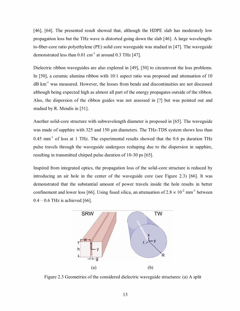
Figure 2.3 Geometries of the considered dielectric waveguide structures: (a) A split
rectangular waveguide and (b) a tube waveguide [66]. .......................................................... 13
Figure 2.4 Schematic of the cross section of a porous terahertz fiber with subwavelength air
holes [52]. ............................................................................................................................. 14
Figure 2.5 Schematic of the plasmonic waveguide. A rectangular groove at the input end is
used to promote coupling in the out-of-plane direction [71]. .................................................. 15
Figure 2.6 Absorption of some dielectrics and semiconductor in THz region. The numbers are
derived from [78]. ................................................................................................................. 17
Figure 3.1 The PPWG supported by PEC and graphene plates (cross section view). The
graphene layer is biased with electric and magnetic fields. The electric field is provided by
applying a gate voltage VG between the graphene and PEC plates and the magnetic field B0 is
considered uniform (brought by an external magnet place below the PEC as illustrated here).
The distance between the plates is assumed to be d. .............................................................. 30
Figure 3.2 The real and imaginary parts of the propagation constant of PEC-graphene and
PEC-conductor (σ=1 s/m) PPWGs. (a) and (b) first three modes (TM0, TM1 and TE1) for the
xi
plate separation of 100 μm (solid line: µc = 0.2 eV, dash line: µc = 0.5 eV and dots: conductor
with σ=1 s/m). (c) and (d) first mode (TM0) for the plate separation of 10 nm and 100 nm. All
in the absence of the external magnetic field . .......................................... 36
Figure 3.3 Real and Imaginary-parts of propagation constants of PPWG with PEC-graphene
walls. These results are derived from solving equation 3.8. The graphene conductivities
derived from equations (1) and (2) assuming . The plate separations are (a), (b)
100 nm and (c), (d) 10 nm. .................................................................................................... 40
Figure 3.4 The proportion of time average power in TE and TM modes for PEC-graphene as a
function of the chemical potential (gate voltage VG) and bias magnetic field at f=100 GHz and
for d=100 nm. ....................................................................................................................... 41
Figure 3.5 The PPWG supported by graphene plates (y-z plane). The graphene layers are
biased with electric and magnetic fields. ............................................................................... 42
Figure 3.6 Real and Imaginary-parts of propagation constants of PPWG with graphene-
graphene walls. These results are derived from solving equation 3.15. The graphene
conductivities derived from equations (1) and (2) assuming . The plate separation
is 100 nm. ............................................................................................................................. 45
Figure 3.7 The proportion of time average power in TE and TM modes for graphene-graphene
as a function of the chemical potential (gate voltage VG) and bias magnetic field at f=100 GHz
and for d=100 nm. ................................................................................................................. 46
Figure 4.1 The dielectric slab waveguide geometry. The wave propagates toward the z
direction. The THz signal will illuminate the side wall of the slab shown by the hatched
circular area. ......................................................................................................................... 54
Figure 4.2 Wave propagation inside two different width size dielectric slab waveguides (d =
200 μm and L = 0.5 mm). (a) ω = 250 μm, S11 = -24 dB and S12 = -0.434 dB, (b) ω = 1 mm,
S11 = -17.9 dB and S12 = -1.94 dB both at f = 1 THz. The HR-silicon is considered to the
electric permittivity of εr = 11.9............................................................................................. 55

xii
Figure 4.3 (a) measurement setup. (b) and (c) demonstration of THz wave meeting the air-
silicon interface. By introducing plano-cylindrical lens, the incident angle θi will decrease
result in poor confinement of THz wave. ............................................................................... 57
Figure 4.4 THz pulses transmitted through the air and silicon waveguides. From bottom to top
travelled in: air, air with absorbers, silicon waveguide with L = 5 mm and L = 10 mm (see
Figure 4.4). The width of the waveguide is w = 15 mm for both cases. The baselines of the
pulses have been offset for clarity. ........................................................................................ 58
Figure 4.5 Measured transmission spectra of reference and transmitted THz signals. From top
to bottom travelled in: air, air in the presence of the absorbers, silicon waveguide with L = 5
mm and L = 10 mm. The width of the waveguide is w = 15 mm for both cases. .................... 58
Figure 55D.1 Electric field distribution of the first four modes inside DRW with . ....... 62
Figure 5.2 (a) Perspective view of the DRW and coordinate system (b) Cross-section of the
guide and ignored boundary condition (in red) and regions (shaded) in Marcatili method. ..... 68
Figure 5.3 Propagation constant of the rectangular DRW surrounded by air calculated with
Marcatili and multiline methods. The required S-matrix in the multi-line method is obtained
from HFSS. and are the propagation constants of the dielectric (HR-silicon) and
surrounded mediums (air), respectively. is 0 when (unguided, in air) and 1
when (all confined in guide).. .............................................................................. 69
Figure 5.4 (a) Perspective view of the DRW and coordinate system (b) Cross-section of the
guide and ignored boundary condition (in red) and regions (shaded) in Marcatili method. ..... 71
Figure 5.5 Normalized propagation constant of the DRW as function of normalized frequency
(a) (b) (c) . The propagation constants are calculated using the
Marcatili method. Optimal single mode propagation is achievable for ......................... 74
Figure 5.6 Normalized propagation constant of the DRW as function of normalized frequency
(a) (b) (c) . The propagation constants are calculated using the
Marcatili method. Optimal single mode propagation is achievable for ......................... 75

xiii
Figure 5.7 Calculated radiated power from bended DRW as function of radius . The
lines L1 and L2 are results for straight guides of equal length (solid line L1 for WR8 and
dashed line L2 for WR5). ...................................................................................................... 77
Figure 5.8 (a) The measurement setup consists of the DRW with its tether lattice support and
rectangular waveguide flanges. Top left: wireframe (cross section) of support and DRW, h is
designed to place the DRW at the center of the rectangular waveguide (b) photo of the setup
for F-band with DRW before connecting the second flange. .................................................. 78
Figure 5.9 Etched angles of the walls of the DRWs due to the DRIE process. The etched angle
is ˚ for WR8 and 1.95˚ for WR5. The dimensions of (a) WR8: atop = 575μm, abottom =
520μm, and b = 590μm and (b) WR5: atop = 375μm, abottom = 345μm, and b = 370μm. .......... 79
Figure 5.10 Measured propagation constant of the DRWs compared with the simulation of the
real structure geometry with sloped walls. ............................................................................. 80
Figure 5.11 Comparison between measured and simulated S-parameters. (a) F- and (b) G-
bands. For both cases the length of the waveguide is 15mm. ................................................. 81
Figure 6.1 The discontinuity topology which can be modelled with K/J invertors and thus the
T/π equivalent circuits. .......................................................................................................... 83
Figure 6.2 (a) Simulation setup and (b) K/Z0 and φ of the impedance invertor and as function
of d for different t values. These values are calculated from the S-parameters obtained from
simulations with HFSS at 120 GHz. ...................................................................................... 87
Figure 6.3 Block diagram of a typical passband filter using impedance invertors................... 87
Figure 6.4 (a) 5th order bandpass filter and (b) Simulation results derived from HFSS. The
dimensions for the 3rd
order filter are t1 = 145, t2 = 90 μm, l1 = 488 μm, l2 = 448 μm and d1 =
d2 = 75μm. Also, for the 5th
order filter the dimensions are t1 = 275 μm, t2 = 290 μm, t3 = 380
μm, l1 = 454 μm, l2 = 447 μm, l3 = 403 μm and d1 = d2 = d3 = 75 μm. .................................... 91
Figure 0.1 The dielectric slab waveguide geometry. The wave propagates toward the z
direction. Theoretically, it is assumed that the guide is infinite along the x direction............ 114

xiv
Figure C.2 Dispersion diagram of the dielectric ribbon waveguide. The dielectric thickness is
(a) d = 100 μm, (b) d = 385 μm and (c) d = 585 μm. ............................................................ 116
xv
LIST OF TABLES
Table 3.1. Comparison between graphene and copper conductivities (DC) ............................ 27
Table 3.2. Attenuation (α dB/μm) of PEC-graphene PPWG with d = 100 nm. ....................... 38
Table 3.3. Attenuation (α dB/μm) of graphene-graphene PPWG with d = 100 nm. ................ 46
Table 5.1. Some key characteristics of dielectric waveguides ................................................ 67
Table 6.1. Definition of two band-pass filters. ....................................................................... 87
1
1 THE TERAHERTZ GAP: “A PART OF
SPECTRUM THAT HAS BEEN LEAST
EXPLORED”
1.1 The THz gap
The terahertz (THz) band does not have a universal definition yet. In some references, it is
applied to sub-millimeter wave range (0.3 - 3 THz) [1, 2], while in others, it refers to the band
that lies between the microwave and the infrared frequency regions of the electromagnetic
spectrum (0.1 - 30 THz) [3]. A 1 THz electromagnetic wave has a period of 1 ps, wavelength
of 300 μm, wavenumber of 33.3 cm-1
, photon energy of 4.14 meV and equivalent temperature
of 48 K. As an electromagnetic wave of any frequency, the Maxwell equations also rule the
terahertz world. However, THz waves are difficult to handle and cannot be treated with
techniques commonly used in the neighborhood bands. For example, realizing efficient and
practical sources and sensors is still a challenge. Hence, the spectrum which is located
between microwave and optics, which are both mature and technologically developed, is
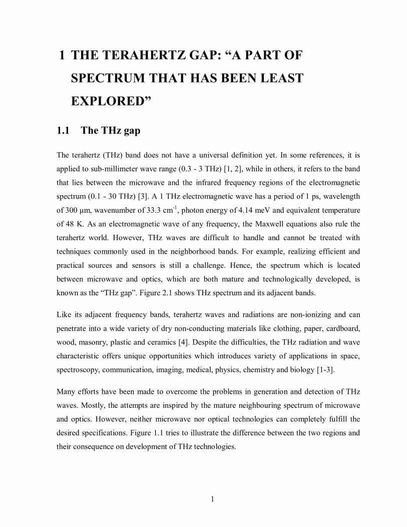
known as the “THz gap”. Figure 2.1 shows THz spectrum and its adjacent bands.
Like its adjacent frequency bands, terahertz waves and radiations are non-ionizing and can
penetrate into a wide variety of dry non-conducting materials like clothing, paper, cardboard,
wood, masonry, plastic and ceramics [4]. Despite the difficulties, the THz radiation and wave
characteristic offers unique opportunities which introduces variety of applications in space,
spectroscopy, communication, imaging, medical, physics, chemistry and biology [1-3].
Many efforts have been made to overcome the problems in generation and detection of THz
waves. Mostly, the attempts are inspired by the mature neighbouring spectrum of microwave
and optics. However, neither microwave nor optical technologies can completely fulfill the
desired specifications. Figure 1.1 tries to illustrate the difference between the two regions and
their consequence on development of THz technologies.
2
Figure 1.1 (Top) THz and its neighbouring frequency bands. (Middle) comparison of
electromagnetic wave generation in RF (left) and optics (right). (Bottom) Some waveguiding
techniques from each neighbouring bands.
1.2 THz Applications
THz applications often exploit the unique signature of substances in this frequency region.
Astronomers look at radiated power in different wavelengths (range of 1 mm to 100 μm) of,
for instance, the interstellar dust to analyse their spectral contents (see Figure 2 of Ref. [4]).
These signals are not detectable with the Earth-based observations, thus, the space
astrophysics instruments are using or will use THz technologies to detect the interstellar or
intergalactic signals [4]. This feature is also used in spectroscopic applications to identify the
materials [4] where the strength of the emission and absorption lines of the molecules, which
tend to increase in strength as f 2 or even f
3, often peaks in the submillimeter. Adding the non-
ionizing and penetrability of THz waves, other application like non-destructive and non-

3
invasive testing and inspection, quality control of pharmaceutical and food and security
control are foreseen.
Considering the never-ending need for bandwidth in mobile traffic, THz communication
seems to be a very good candidate for future systems providing 10 Gb/s data rate [5].
However, the atmospheric attenuation and group velocity dispersion (GVD) are the main
drawbacks for THz communication. Regarding only the attenuation of atmosphere for
frequencies above 1 THz, it is somewhat impossible to make a long haul communications.
Also, due to the rain and other weather conditions attenuations, it seems that the THz
communication will be bound to indoor links [5]. These systems can be used for secure
communications, e.g. for battle field applications, or for huge throughputs in mobile handsets
[5]. For instance, in [6, 7], a 167 m atmosphere link with 51% relative humidity at 21 °C is
realized and signal to noise ratio of 200 is measured.
1.3 THz generation and detection
THz sources are based either on down conversion of laser pulses or up conversion of
microwave continuous-wave (CW) signals. Down conversion technique is implementable by
using photoconductive (PC) antennas excited by a pulsed laser beam. Also, mixing two laser
beams with different frequencies (ωT = ω2 – ω1) is another way to generate THz signal. The
later will produce a continuous wave THz signal while the former will for generate wide band
pulsed THz signals. On the other hand, from the microwave side, schottky diodes were used to
up convert a microwave source to a continuous wave THz signal.
The pulsed THz wave emitter and detector were, for the first time, introduced in the late 1980s
by the means of PC antennas [8, 9]. The PC antenna emitters are capable of providing 40 μW
and bandwidth of 10 THz [10, 11]. Optical rectification, which is based on the inverse process
of the electro-optic (EO) effect, is the other common technique for the generation of the THz
pulses [12]. The bandwidth of optical rectification based emitters can reach to 100 THz, as the
pulse comes directly from the laser (not by the response of the material) [13-15].
Time domain spectroscopy (TDS) is the most well-known THz pulsed generation and
detection technique that may use EO crystals or PC antennas [16]. It is used to image an object
4
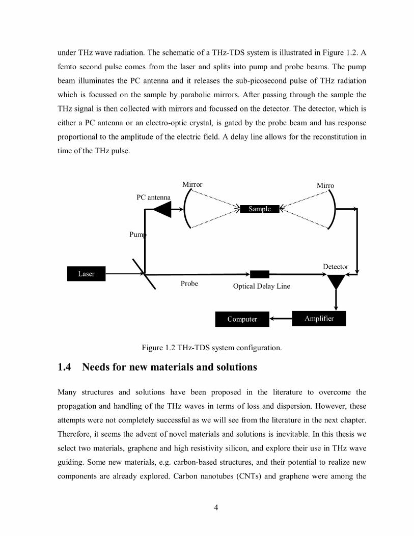
under THz wave radiation. The schematic of a THz-TDS system is illustrated in Figure 1.2. A
femto second pulse comes from the laser and splits into pump and probe beams. The pump
beam illuminates the PC antenna and it releases the sub-picosecond pulse of THz radiation
which is focussed on the sample by parabolic mirrors. After passing through the sample the
THz signal is then collected with mirrors and focussed on the detector. The detector, which is
either a PC antenna or an electro-optic crystal, is gated by the probe beam and has response
proportional to the amplitude of the electric field. A delay line allows for the reconstitution in
time of the THz pulse.
Figure 1.2 THz-TDS system configuration.
1.4 Needs for new materials and solutions
Many structures and solutions have been proposed in the literature to overcome the
propagation and handling of the THz waves in terms of loss and dispersion. However, these
attempts were not completely successful as we will see from the literature in the next chapter.
Therefore, it seems the advent of novel materials and solutions is inevitable. In this thesis we
select two materials, graphene and high resistivity silicon, and explore their use in THz wave
guiding. Some new materials, e.g. carbon-based structures, and their potential to realize new
components are already explored. Carbon nanotubes (CNTs) and graphene were among the
Laser
Optical Delay Line
Sample
PC antenna
Mirror Mirro
r
Amplifier
Detector
Computer
Probe
Pump
5
candidates according to their unique electronic properties [17]. Carbon nanotube can have
either metallic or semiconductor characteristics by using single-walled nanotube (SWNT) or
multi-walled nanotube (MWNT), respectively [17]. Therefore, CNTs have been used to realize
different passive (e.g. antennas [18]) and active components (e.g. field-effect transistors [19]).
However, THz and Microwave applications of graphene layers have not yet been extensively
explored, mainly due to the small size of the layers available until recently. Thereafter, we
investigated the performance of high resistivity silicon in THz region. The results demonstrate
that the high resistivity silicon ribbon waveguide can be the superior guiding mechanism in
THz region.
1.5 Thesis outline
This thesis includes seven chapters structured on three published articles. The state of art is
presented in chapter 2, which also includes the overall scientific notions required to
understand the subsequent chapters. The project definition and objectives are also discussed in
the named chapter. Chapter 3 covers the results of studying parallel plate waveguide with
anisotropic graphene plates. These graphene plates are biased by electric and magnetic fields.
The closed form dispersion equations are derived and numerically solved. The unique
properties of graphene lead to a waveguide with mode selection capability for THz band
region. Afterward, in chapter 4, 5 and 6, HR-silicon is considered and studied as another
material for THz wave guiding. Chapter 4 covers the simulation and characterization of
dielectric slab waveguide made of HR-silicon. The slab guide is characterized with THz-TDS
system. Chapter 5 describes the detailed design and simulation of dielectric ribbon waveguide.
This structure is fabricated using microfabrication techniques and characterized by an Agilent
PNA-X network analyser with Virginia Diodes Inc.'s (VDI) extension modules. Chapter 6
focuses on THz filter design based on HR-silicon the dielectric ribbon waveguide described in
chapter 5. Design method and fabrication process for third and fifth order bandpass filters are
provided for F/G-band regions. Lastly, Chapter 7 provides conclusions and suggestions for
future work.
6
2 STATE OF THE ART: NOVEL MATERIALS
FOR TERAHERTZ WAVEGUIDING
Although the THz spectrum attracted extensive attention during the past decade, guiding the
THz wave is still a challenge. Many waveguide structures, both inspired from microwave and
infrared/optic regions, have been proposed to fulfill the application specifications. However,
both categories didn’t succeed to bring a suitable technology addressing the major hitches.
Although, some of the proposed designed configurations managed to overcome the loss and
dispersion problems, a few drawbacks like integrability, fabrication cost and feasibility of
realization of other passive components still remain. Looking into the current technologies and
their problems, the incapacity of the current state of the art is evident. The need of new
materials and solutions is inevitable. In this chapter, we will take a look at the current state of
the art guiding mechanisms and technologies in THz region and discuss their pros and cons.
Thereafter, we will talk about the new possible material solutions that will be discussed, in
more details, in the next chapters.
2.1 THz Wave Guiding Technology
The waveguides derived from the microwave part of the spectrum are mainly hollow metallic
guides. In contrast, those transferred from the optical/infrared region are generally made of
dielectrics. The main concerns are propagation losses (including ohmic, absorption and
radiation losses). In metallic waveguides the ohmic losses are dominant, while on the other
hand, in dielectric structures absorption is the leading loss mechanism. The power losses are
expressed in cm-1
[21]. The power propagation loss, α, can also be expressed in [dB/cm] by
the following equation (inspired from [21])
[
] [ ] [ ] 2.1

7
In the following sub-sections the current state of the art of the metallic and dielectric
waveguides and their weaknesses and strength are studied.
2.1.1 Metallic Waveguides
Many guiding mechanisms have been studied as potential candidates for low-loss, low-
dispersive THz interconnects. Classic metallic waveguides which have been extensively used
in microwave region were evaluated for THz propagation by many researchers [22-37]. In
1991, M. Y. Frankel demonstrated that a coplanar waveguide (CPW) and a coplanar strip
(CPS) which are printed on GaAs and sapphire, respectively, have 2.5 mm-1
and 2 mm-1
loss at
1 THz [22]. Circular and rectangular metallic waveguides (so-called metallic hollow core
waveguides) were also investigated in [23], [24]. Beyond the ohmic losses of 7 mm-1
at 1 THz,
those hollow core waveguides were highly dispersive near the cutoff frequencies. This can be
proved by looking at the group velocity of rectangular waveguides which can be derived from
[38]
[ ( )
]
⁄
2.2
At the cutoff frequency (where f = fc), the group velocity is equal to the speed of light. As the
frequency increases the group velocity becomes less than the speed of light. This frequency
dependence leads to the dispersion of traveling signal down the waveguide. Assuming a
rectangular waveguide with length L, a wave with frequency f0 needs L/VGroup seconds, so-
called group delay, to propagate down the waveguide. However, this group delay changes for
adjacent frequencies. Using equation 2.2 one can write differential changes in group delay as
[ (
)
]
2.3
where Tg= L/VGroup is the group delay. From equation 2.3 it can be observed that at close to the
cutoff frequency the group delay changes drastically representing the dispersive nature of the
8
guide. It is worth noting that in the case of THz applications, we mainly talk about
spectroscopy where we need the widest possible bandwidth (e.g. 0.3 – 3 THz). Therefore,
although the same equation applies for both the microwave and THz bands but in the
microwave the applications are limited to specific bands. For instance, the WR-90 waveguides
are employed for X-band not for the entire microwave frequency band (e.g. from 0.1 – 30
GHz).
Considering the losses and generally speaking, the performance of hollow core metallic
waveguides is much better than the coplanar guides and microstrips [24]. High losses in
coplanar transmission lines, in comparison with hollow cores, are due to three loss
mechanisms: ohmic losses in the metal strips, dielectric losses in the substrate, and radiation
losses due to fringing fields.
In hollow core waveguides, ohmic losses linked to the normal electric field at the conductor-
air boundary are the source of attenuation. Therefore, keeping the propagating wave power far
from the metallic side walls can reduce the losses [25]. In other words, in hollow cores the
losses are inversely related to the core diameter. More precisely, the attenuation is
proportional to the inverse third power of the guide diameter (
) [20, 26]. Although,
increasing the waveguide diameter can decrease the wave attenuation, it will enable multi-
mode propagation and therefore enhance dispersion. Hollow cores with large core diameter
(larger than the wavelength) has evolved by covering the inner metallic surface with a thin
dielectric layer [27, 28]. As shown in [20], small losses in the range of 1 dB/m, small
dispersion which is independent from the dielectric coating material and efficient coupling of
the dominant mode are achieved for these guiding structures.
New fabrication methodologies and techniques for standard hollow-cores waveguides and
filters were studied recently in [39]. The measurement and calibration techniques are
developed for these waveguides and adapted to the THz region [40, 41]. The repeatability and
mismatch of waveguide flange connections is another issue of hollow core waveguides which
was studied in [42].
Parallel plate waveguide (PPWG) is another sort of metallic guiding structures. PPWGs can
support TEM, TM and TE modes. In TEM modes, the electric field is distributed uniformly
9
between the plates. Therefore, one can expect moderately high loss for TEM mode as
discussed in [29, 30]. A PPWG excited by TEM mode shows 0.5 - 2 mm-1
attenuation in the
0.5 - 3 THz frequency band [29]. Also, THz pulses become broader after propagating inside
the waveguide which is due to frequency dependence loss despite a negligible group velocity
dispersion [29].
Unlike TEM modes, the TE1 mode, in which the electric fields vanish at metallic plates, has
lower ohmic losses. As studied in [31, 32], the attenuation of PPWG with 0.5 mm plate
separation for TEM and TE1 modes is 0.023 and 5.7×10⁻⁴
mm-1
at 1 THz, respectively [31].
One should note that the difference between the reported results in [29] and [31] is due to
different plate separations that they used (90 μm in [29] and 0.5 mm in [31]). Like hollow core
structure, increasing the plate separation will decrease the loss at the expense of introducing
higher modes [30, 33].
Due to their low-loss and low-dispersive characteristics, PPWGs attract many researchers. A
PPWG which incorporated quasi-optical elements was proposed (see Figure 2.1 (a)) in [34]. It
was shown that, the mirrors have a minimal effect on the overall loss of the transmission line
and the dominant mode were still TEM, for significant length of propagation and multiple
reflections [34]. Also, a THz transmitter which was integrated inside a PPWG is studied in
[35]. The PPT transmitter was realized by using the PPWG metallic plates as means of
applying a bias voltage while layer of semi-insulating gallium arsenide lies between [35].
Metal wires (Figure 2.1 (b)) demonstrate substantially lower loss in comparison with other
metallic waveguides and almost no dispersion [36]. This is related to the low exposure of the
metal to THz wave which propagates as a weakly guided radial surface waves. In [36], it is
shown that a 0.9 mm diameter stainless steel wire has an attenuation of less than 3.0 × 10⁻³
over 0.25 – 0.75 THz. However, the waveguide suffers from radiation losses at bends or
discontinuities.
As mentioned earlier, the metal wires are low loss structures due to their loose confinement of
the electric field. Increasing the wave confinement is possible but it results in more exposure
of the metal to THz wave. In other words, “there is a fundamental trade-off between strong
mode confinement and low attenuation characteristics for metallic waveguides” [37]. One

10
solution, as suggested in [37], is to use the dual configuration of the metal wires (so-called
metallic slit waveguide) shown in Figure 2.1 (c). The suggested structure consists of two
metallic slabs separated by a slit and surrounded by air. This guiding structure shows less than
5.7 × 10⁻²
mm-1
at 0.1 – 1 THz frequency band and almost zero dispersion [37].
(a)
(b)
(c)
Figure 2.1 (a) THz-TDS arrangement of the parallel plate structure incorporating four
reflections [34]. (b) The diagram of the optical set-up and coupling mechanism of the
propagating mode on a metal wire waveguide [36]. (c) Metallic slit waveguide and two-
dimensional distribution of the electric field amplitude [37].
2.1.2 Dielectric Waveguides
Unlike the metallic structures in which confinement and propagation down the guide is due to
metallic reflection from the walls, dielectric waveguides have different type of propagation
mechanisms including total internal reflection, antiresonance and photonic bandgap. Recently,
11
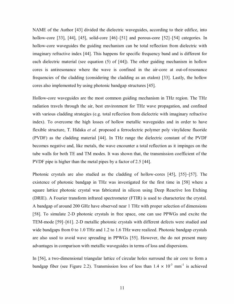
NAME of the Author [43] divided the dielectric waveguides, according to their edifice, into
hollow-core [33], [44], [45], solid-core [46]–[51] and porous-core [52]–[54] categories. In
hollow-core waveguides the guiding mechanism can be total reflection from dielectric with
imaginary refractive index [44]. This happens for specific frequency band and is different for
each dielectric material (see equation (5) of [44]). The other guiding mechanism in hollow
cores is antiresonance where the wave is confined in the air-core at out-of-resonance
frequencies of the cladding (considering the cladding as an etalon) [33]. Lastly, the hollow
cores also implemented by using photonic bandgap structures [45].
Hollow-core waveguides are the most common guiding mechanism in THz region. The THz
radiation travels through the air, best environment for THz wave propagation, and confined
with various cladding strategies (e.g. total reflection from dielectric with imaginary refractive
index). To overcome the high losses of hollow metallic waveguides and in order to have
flexible structure, T. Hidaka et al. proposed a ferroelectric polymer poly vinylidene fluoride
(PVDF) as the cladding material [44]. In THz range the dielectric constant of the PVDF
becomes negative and, like metals, the wave encounter a total reflection as it impinges on the
tube walls for both TE and TM modes. It was shown that, the transmission coefficient of the
PVDF pipe is higher than the metal pipes by a factor of 2.5 [44].
Photonic crystals are also studied as the cladding of hollow-cores [45], [55]–[57]. The
existence of photonic bandgap in THz was investigated for the first time in [58] where a
square lattice photonic crystal was fabricated in silicon using Deep Reactive Ion Etching
(DRIE). A Fourier transform infrared spectrometer (FTIR) is used to characterize the crystal.
A bandgap of around 200 GHz have observed near 1 THz with proper selection of dimensions
[58]. To simulate 2-D photonic crystals in free space, one can use PPWGs and excite the
TEM-mode [59]–[61]. 2-D metallic photonic crystals with different defects were studied and
wide bandgaps from 0 to 1.0 THz and 1.2 to 1.6 THz were realized. Photonic bandgap crystals
are also used to avoid wave spreading in PPWGs [55]. However, the do not present many
advantages in comparison with metallic waveguides in terms of loss and dispersions.
In [56], a two-dimensional triangular lattice of circular holes surround the air core to form a
bandgap fiber (see Figure 2.2). Transmission loss of less than 1.4 × 10⁻³
mm-1
is achieved

12
between 1.55 – 1.85 THz [56]. The suggested waveguide demonstrated a low loss
characteristic due to propagation in air and low scattering losses in THz region [62].
In [57], methylpentene polymer was used to realize an air-rod holes photonic crystal. The
polymer has a dielectric constant of 2.1 and is almost lossless in the THz region [57]. The
photonic crystal specimen was fabricated by stacking ten 0.5 mm thick plates. Holes were
made using numerically controlled milling machine and the plates are stacked by using four
metal pins in each corner [57]. It was found that the transmitted wave’s phase changes by π for
each crystal plane (for n crystal planes along the direction of the incident wave the phase
should change by nπ across the band) [57].
Figure 2.2 Cross section of an air-core terahertz photonic band-gap fiber [56].
Solid core waveguides have air (e.g. [46]) or photonic crystal clads (e.g. [48]) where the
guiding mechanism is based on total internal reflection. Although the losses of hollow-core
structures are generally lower, solid-cores are easier and cheaper to fabricate. In solid cores
THz wave propagates inside the core region thus the absorption coefficient of the core
material becomes more significant. These waveguides are normally made of the polymers
which demonstrate a low absorption in THz region [63]. At the same time, the fabrication of
the polymer waveguides is easier in comparison with the others. Therefore, plenty of
researches are dedicated to finding low-loss and low-dispersive material to be used as the core
in these waveguides. In [46], a slab of high-density polyethylene (HDPE) is scrutinized using
THz-TDS system. It is claimed that, the TEM (TM0) mode is the dominant propagating mode,
although the input signal extends beyond the cutoff frequencies of several higher order modes
13
[46], [64]. The presented result showed that, although the HDPE slab has moderately low
propagation loss but the THz wave is distorted going down the slab [46]. A large wavelength-
to-fiber-core ratio polyethylene (PE) solid core waveguide was studied in [47]. The waveguide
demonstrated less than 0.01 cm-1
at around 0.3 THz [47].
Dielectric ribbon waveguides are also explored in [49], [50] to circumvent the loss problems.
In [50], a ceramic alumina ribbon with 10:1 aspect ratio was proposed and attenuation of 10
dB km-1
was measured. However, the losses from bends and discontinuities are not discussed
although being expected high as almost all part of the energy propagates outside of the ribbon.
Also, the dispersion of the ribbon guides was not assessed in [?] but was pointed out and
studied by R. Mendis in [51].
Another solid-core structure with subwavelength diameter is proposed in [65]. The waveguide
was made of sapphire with 325 and 150 μm diameters. The THz-TDS system shows less than
0.45 mm-1
of loss at 1 THz. The experimental results showed that the 0.6 ps duration THz
pulse travels through the waveguide undergoes reshaping due to the dispersion in sapphire,
resulting in transmitted chirped pulse duration of 10-30 ps [65].
Inspired from integrated optics, the propagation loss of the solid-core structure is reduced by
introducing an air hole in the center of the waveguide core (see Figure 2.3) [66]. It was
demonstrated that the substantial amount of power travels inside the hole results in better
confinement and lower loss [66]. Using fused silica, an attenuation of 2.8 × 10⁻²
mm-1
between
0.4 – 0.6 THz is achieved [66].
(a) (b)
Figure 2.3 Geometries of the considered dielectric waveguide structures: (a) A split

14
rectangular waveguide and (b) a tube waveguide [66].
Although there is high THz absorption in water vapour, air propagation is still the best
environment for THz waves, in comparison with polymers, semiconductors and dielectrics.
Therefore, to maximize the “in air” propagation a category of waveguides (so-called porous
fibers) are suggested by and shown in Figure 2.4 [52]–[54]. In these structures, subwavelength
air holes are created within the core of solid-core guide. Material losses are expected to
decrease as the fraction of the air holes to core material increase (this fraction is limited by
fabrication constraints). In [52], numerical results showed that the larger part of energy
propagates inside the air holes. This improved the absorption loss by a factor of ~ 10 – 20
[52]. In [52], total fiber loss of less than 1.1 × 10⁻³
mm-1
at 1 THz was predicted. It also has
been shown that for similar diameter, porous fibers offer better confinement and consequently
lower bend losses. Also, planar porous dielectric waveguides were proposed, fabricated and
characterized in view of their potential applications as low-loss waveguides and sensors in the
THz spectral range in [67]. It was shown that, the planar porous waveguide exhibits
considerably smaller transmission losses than a bulk material [67].
Figure 2.4 Schematic of the cross section of a porous terahertz fiber with subwavelength air
holes [52].
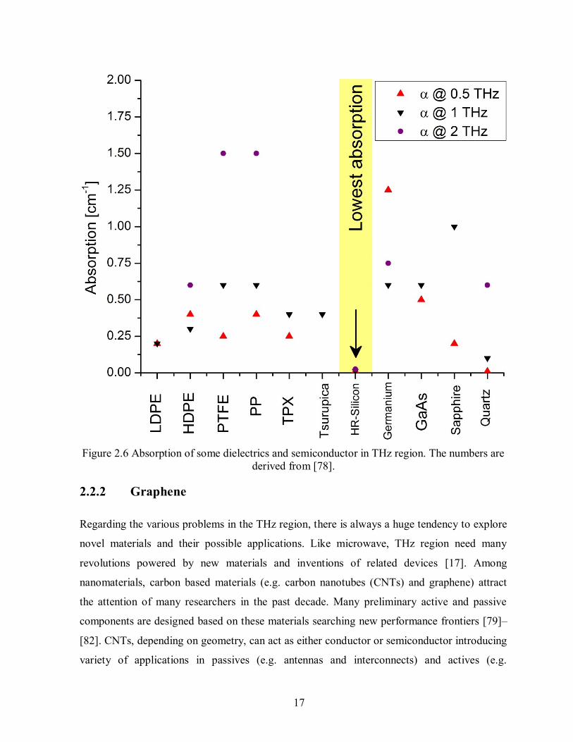
Finding a highly transparent material in THz region is the most crucial part of solid core
dielectric waveguide design. Some types of materials are highly transparent in the THz region
including polymers, dielectrics and semiconductors [63]. Polymers such as polyethylene,
Teflon (PTFE), and TPX are transparent and almost dispersionless at THz frequencies [63]
(see Figure 2.2). In dielectrics and semiconductors high-resistivity silicon attracts the
researchers. High-resistivity float-zone mono-crystalline silicon shows high transparency and
15
low dispersion in THz region [68], [69] (see Figure 2.2). In [53], it is shown that the HR-
silicon is one of the potential candidates since its absorption coefficient is estimated to be less
than 0.087 dB/cm (0.01 cm-1
) over the entire range of 0.1-1 THz. Also, the index of refraction
varies only by 0.0001 over this frequency range [69] which suggests very low dispersion
properties of the HR-silicon. This low dispersion characteristic is experimentally demonstrated
in Chapter 4 where we characterized a HR-silicon slab waveguide using THz-TDS system
[21].
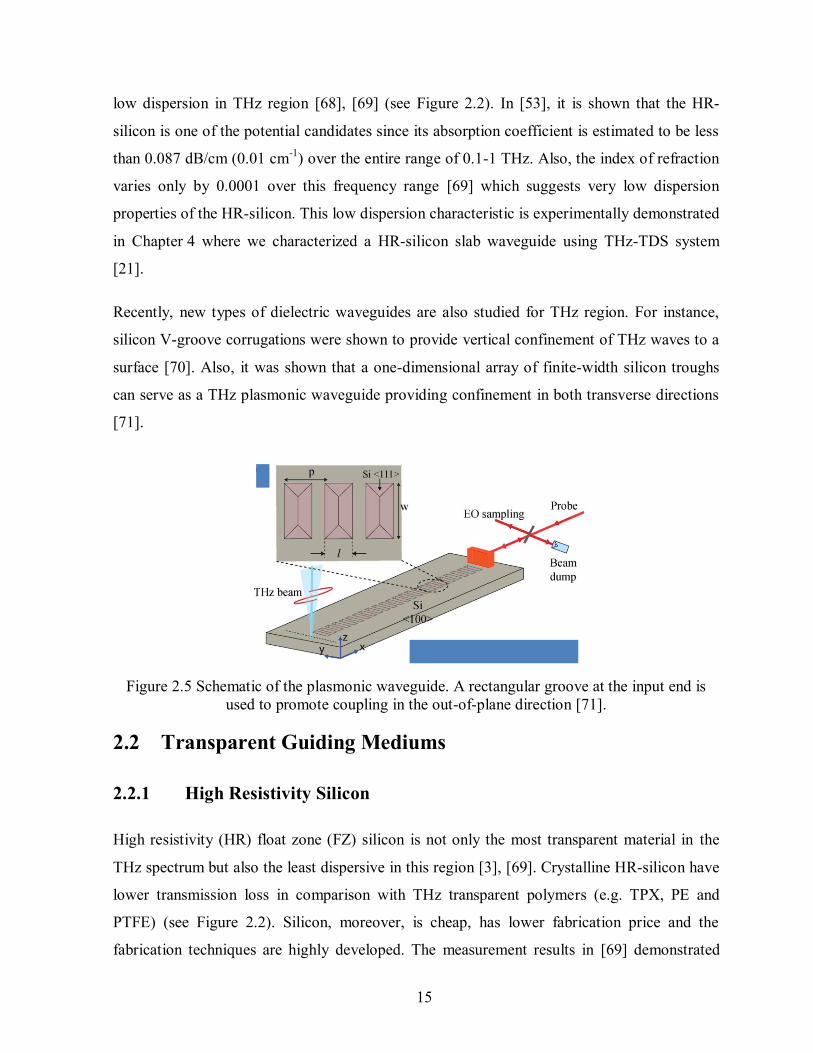
Recently, new types of dielectric waveguides are also studied for THz region. For instance,
silicon V-groove corrugations were shown to provide vertical confinement of THz waves to a
surface [70]. Also, it was shown that a one-dimensional array of finite-width silicon troughs
can serve as a THz plasmonic waveguide providing confinement in both transverse directions
[71].
Figure 2.5 Schematic of the plasmonic waveguide. A rectangular groove at the input end is
used to promote coupling in the out-of-plane direction [71].
2.2 Transparent Guiding Mediums
2.2.1 High Resistivity Silicon
High resistivity (HR) float zone (FZ) silicon is not only the most transparent material in the
THz spectrum but also the least dispersive in this region [3], [69]. Crystalline HR-silicon have
lower transmission loss in comparison with THz transparent polymers (e.g. TPX, PE and
PTFE) (see Figure 2.2). Silicon, moreover, is cheap, has lower fabrication price and the
fabrication techniques are highly developed. The measurement results in [69] demonstrated

16
that the index of refraction changes only 0.0001 over the range of 0.5 – 4.5 THz showing
dispersionless behavior of HR-silicon. Also, the absorption is measured to be less than 0.01
cm-1
at 1 THz (see Figure 5 of [69]). Moreover, high resistivity silicon was widely used in
realization of traditional rectangular waveguide components at sub-millimeter frequencies due
to its low cost micromachining process [72]–[75]. In [72], a first characterization of the silicon
rectangular waveguide was presented at 400 GHz. The silicon rectangular waveguide was
made using lithography, DRIE and metallization techniques [72]. The efforts were continued
by design and fabrication of waveguide components for the 325-500 GHz in [73]. The
integration of other active components for WR1.5 was discussed in [74]. Due to the alignment
problems at high frequencies, a pin system is developed in [75] to improve the wafer-to-wafer
alignment.
Other components such as frequency selective surfaces (FSSs) for quasi-optical filters, to
suppress harmonic in submillimeter and THz frequency band, was fabricated on HR-silicon
substrate and experimentally studied in [76]. In [77], planar Goubau line is fabricated on HR-
silicon substrate to decrease the losses of the line for THz applications. It is also used as the
host material for realization of other metallic components (e.g. hollow metallic waveguides)
according to its easy and precise fabrication process (especially DRIE). However, its guiding
properties didn’t scrutinize yet.
17
Figure 2.6 Absorption of some dielectrics and semiconductor in THz region. The numbers are
derived from [78].
2.2.2 Graphene
Regarding the various problems in the THz region, there is always a huge tendency to explore
novel materials and their possible applications. Like microwave, THz region need many
revolutions powered by new materials and inventions of related devices [17]. Among
nanomaterials, carbon based materials (e.g. carbon nanotubes (CNTs) and graphene) attract
the attention of many researchers in the past decade. Many preliminary active and passive
components are designed based on these materials searching new performance frontiers [79]–
[82]. CNTs, depending on geometry, can act as either conductor or semiconductor introducing
variety of applications in passives (e.g. antennas and interconnects) and actives (e.g.

18
transistors and diodes). Graphene, a 2D hexagonal lattice of carbon atoms, demonstrates
unique electrical and mechanical properties such as high mobility (can exceed 15,000 cm2V
-1s
-
1 under ambient conditions), Hall Effect at room temperature and tunability (by applied gate
voltage). Several components such as frequency selective surfaces [83], [84], antennas [85]–
[87], waveguides [88], [89], filters [90] and lenses [91], [92] are proposed and studied.
Many antenna configurations with different capabilities were proposed based on graphene
(e.g. [85] and [86]). In some designs the graphene layer is a radiating element [85], while in
others it used as parasitic element [86]. For instance in [86], a dipole antenna was printed on
the layer of graphene. The radiation pattern of the dipole changed by the varying of graphene
conductivity using a gate voltage [86]. Also, a switchable high impedance surface (HIS) was
realized, using single layer of graphene, and incorporated to develop a beam reconfigurable
antenna [87]. Simulation results were demonstrated that the beam of the suggested antenna can
scan ±30˚ [87]. A graphene leaky wave antenna, with beam scanning capabilities, was
designed and analyzed [85]. The designed antenna consists of a graphene sheet mounted on a
back-metallized substrate and a set of DC gating pads to control the conductivity of each
graphene section located beneath it [85].
Graphene is also employed to reach special guiding properties mostly in THz region (e.g. [88],
[89]). Shapoval, et al. investigated the plane wave scattering and absorption by infinite and
finite gratings of free space standing infinitely long graphene strips at THz frequencies [89].
Surface plasmon modes supported by graphene ribbon waveguides were also studied [93]. The
propagation of surface waves along single and parallel plate waveguides with graphene sheets
were studied in the absence of magnetic field [88]. The per unit length equivalent circuit of the
proposed waveguides were derived and discussed [88].
19
3 PARALLEL PLATE WAVEGUIDE WITH
GRAPHENE PLATES
3.1 Avant-propos
Auteurs et affiliation:
Ali Malekabadi : étudiant au doctorat, Université de Sherbrooke, Faculté de génie,
Département de génie électrique.
Serge A. Charlebois : professeur, Université de Sherbrooke, Faculté de génie,
Département de génie électrique.
Dominic Deslandes : professeur, Université de Québec à Montréal, Faculté de génie,
Département de génie électrique.
Date d’acceptation: 21 janvier 2013
État de l’acceptation: version finale publiée
Revue: Journal of Applied Physics
Référence: [94]
Titre français: Guides d'ondes à plaques parallèles constituées de graphène anisotropique:
effet d'un champ électrique et d'un champ magnétique externe.
Contribution à la thèse:
Le graphène semble présenter de nombreuses caractéristiques physiques qui pourraient être
utilisées dans de nombreux domaines. Dans cet article, on utilise une couche de graphène
comme condition aux limites pour former un guide d'onde. Les résultats obtenus, bien que ne
s'appliquant pas directement au térahertz sont toutefois remarquables et sont donc présentés.
D'une part, on a démontré pour la première fois la réalisabilité d'un tel guide et la propagation
d'un mode dans ce guide. Mais l'aspect très innovateur vient des propriétés de graphène en lui

20
même. Effectivement, par excitation électromagnétique extérieure, on peut contrôler le type de
mode se propageant, soit les modes TE ou TM, ou bien TE et TM simultanément conduisant à
un mode hybride HE. Ce dernier est obtenu lorsque le champ externe appliqué au graphène est
à la fois électrique et magnétique. D'autre part, on montre que l'intensité de chacune des
composantes du mode HE, soit les composantes TE et TM sont directement contrôlables par
l'intensité des champs externes, ce qui pave la voie à des composants à fonction contrôlable
comme des déphaseurs et des fonctions de rotation des modes. Il est à noter que le
développement mathématique réalisé pour résoudre les équations de Maxwell en présence du
graphène fait intervenir un tenseur de conductivité, tenseur pris de façon générale permettant
en fait d'analyser n'importe quel matériau, isotrope ou anisotrope, en présence de l’effet Hall.
Résumé français :
Les performances d'un guide à plaques parallèles composées soit d'un mur électrique parfait
(PEC) et de graphène, soit de deux films de graphène sont étudiées. Le comportement du
graphène est modélisé comme un milieu anisotrope avec un tenseur de conductivité dont les
éléments de la diagonale et les éléments croisés (conductivité de Hall) sont dérivés des
formules de Kubo. Les modes pouvant exister dans ces deux types de guide à plaques
parallèles sont analysés en résolvant les équations de Maxwell avec une condition aux limites
constituée du graphène soumis soit à un seul champ électrique soit à un champ électrique et un
champ magnétique. Il est démontré que lorsque le graphène est soumis à la fois à un champ
électrique et à un champ magnétique, un mode hybride HE, constitué de la superposition d'un
mode transverse électrique TE et d'un mode transverse magnétique TM, se propage dans le
guide d'onde. L'intensité de chacun des modes TE et TM peut être ajustée selon l'intensité des
champs externes appliqués. L'étude de différents guides montre aussi qu'en diminuant l'espace
entre les deux plaques, un meilleur confinement de l'onde est obtenu. Ce faisant, l'atténuation
de l'onde augmente également. Aussi, un meilleur confinement de l'onde peut-être obtenu en
insérant une couche de diélectrique entre les deux plaques. La procédure analytique utilisée est
générale et peut-être appliquée à d'autres structures guidantes ayant des plaques quelconques à
conductivités isotrope ou non.
Discussion
21
In this chapter, we studied the performances of a parallel plate waveguide (PPWG) supported
by perfect electric conductor (PEC)-graphene and graphene-graphene plates by solving the
Maxwell’s equations inside the structure and applying the boundary conditions while the
graphene layers are biased with both electric and magnetic fields simultaneously. The
graphene plate behavior is modeled as an anisotropic surface with both diagonal and Hall
conductivities derived from Kubo formula. The main difference between this work and other
researches on applications of graphene at microwave and terahertz frequencies (e.g. [95] and
[96]) is, for instance in [95], the use of Dyadic Green’s functions to represent the anisotropic
surface conductivity of the biased graphene. Effects due to magnetostatic bias fields, which
lead to a tensor conductivity were discussed. Also in [96], an exact solution was obtained for
the electromagnetic field due to an electric current in the presence of a surface conductivity
model of graphene. The solution of plane wave reflection and transmission was presented, and
surface wave propagation along graphene was studied in [96]. However, neither [95] and [96]
nor any other publication discussed the wave propagation characteristics inside a PPWG with
graphene plates while they are biased with both electric and magnetic fields simultaneously.
One should note that, by the word “anisotropic” we mean that the graphene sheet was modeled
as an infinitesimally-thin non-local two-sided surface characterized by a surface conductivity
tensor (
). In the only presence of an electric field, the graphene sheet is
characterized by a complex surface conductivity . In the case of graphene layer
biased with both electric and magnetic fields, the electric current density (Js) will have two
components (Jsx and Jsy). Each of the electric current density components will be related to the
x- and y- components of the electric field through the conductivity tensor. Therefore, the
boundary conditions change as described in equation 3.7 unlike in the isotropic mediums (J =
σ E) where J is in the direction of the electric field. We show that this results in hybrid TE-TM
modes propagating inside the waveguide. In the isotropic case (no magnetic field or negligible
Hall conductivity), the boundary conditions can be satisfied by either only TE or TM modes.
A fascinating property of graphene is the possibility to continuously drive the Fermi level
from the valence to the conduction band simply by applying a gate voltage Vg (see Figure
3D.1) resulting in a pronounced ambipolar electric field effect. As the Fermi level is driven
22
inside the conduction (valence) band, the conductivity σ increases with increasing the
concentrations of electrons (holes) induced by positive (negative) gate voltages. The upper
limit for increasing the gate voltage is leakage or arching and is depend on many parameters
including substrate, width of the graphene layer and the synthesis technique used. However,
the burnout reason is most likely charged impurities from the surface of the exposed graphene
which are expelled by very high fields. This limitation for Vg is different from sample to
sample and thus difficult to have an accurate prediction.
Increasing the applied gate voltage Vg, will increase the diagonal conductivity of graphene σd.
Therefore, the attenuation of the waveguide decreases. By increasing the bias magnetic field
B0, in specific frequency the Hall conductivity σh will increase while the diagonal conductivity
will decrease. Hence, by applying mode magnetic fields the waveguide will produce more
losses.
Regarding the discussion on wave confinement linked to real part of the slow wave factor
(SWF), we would like to emphasize on the difference of our analysis with conventional
metallic PPWGs. In the latter, one considers only propagating medium between and reflection
on the plates. Therefore, the confinement is always guaranteed. In our case the wave equation
is solved in all three mediums surrounding the PPWG structure and the boundary conditions
(as described in equation 3.7) represent the plates. In this case, the wave confinement is not
guaranteed and certain conditions should be met for effective confinement. The real part of the
SWF being more than 1 is certainly one of those conditions.
Here, we studied the PPWG with different plate separations (d = 10 nm and 100 nm). These
small values of d resulted in highly confined modes and, at the same time, large attenuation
values. As in this dissertation, we have shown the influence of different waveguide parameters
and bias fields on its performance and studied their trends, proper selection of plate separation
or other parameters will be application specific and is the subject of further investigations.

23
Figure 3D.1 Different possible PEC/conductor-graphene and graphene-graphene PPWGs .
24
3.2 Parallel plate waveguide with anisotropic graphene plates:
effect of electric and magnetic biases
3.2.1 Abstract
The performances of a parallel plate waveguide (PPWG) supported by perfect electric
conductor (PEC)-graphene and graphene-graphene plates are evaluated. The graphene plate
behavior is modeled as an anisotropic medium with both diagonal and Hall conductivit ies
derived from Kubo formula. The PPWG modes supported by PEC-graphene and graphene-
graphene plates are studied. Maxwell’s equations are solved for these two waveguides while
the graphene layers are biased with an electric field only and with both electric and magnetic
fields. It is shown that when both electric and magnetic biases are applied to the graphene a
hybrid mode (simultaneous TE and TM modes) will propagate inside the waveguide. The
intensity of each TE and TM modes can be adjusted with the applied external bias fields.
Study of different waveguides demonstrates that by decreasing the plate separation (d), the
wave confinement improves. However, it increases the waveguide attenuation. A dielectric
layer inserted between the plates can also be used to improve the wave confinement. The
presented analytical procedure is applicable to other guiding structures having walls with
isotropic or anisotropic conductivities.
3.2.2 Introduction
Although it was not expected to exist in nature, a two-dimensional (2D) atomic layer of carbon
was experimentally discovered in 2004. Novoselov et al., have demonstrated that a few layers
of graphene behave like a conductor and are stable under ambient conditions [97]. With a
thickness of 0.34 nm, this 2D honeycomb lattice of carbon atoms demonstrates promising
properties, such as high carrier mobility, thus opening a new window to high-speed nano-
electronics. Other 2D atomic crystals were investigated and their electronic properties were
compared with graphene in [98].
Electric field effect experiments on graphene reveal an ambipolar behavior similar to that
observed in semiconductors [97]. The charge carrier density can be tuned continuously
25
between electrons and holes [99], [100] thus enabling a control on the electronic properties of
graphene by applying an external voltage. The carrier concentration can reach as much as
1013
cm-2
and the motility of both electrons and holes can exceed 15,000 cm2V
-1s
-1, even under
ambient conditions [99]. Also, the mobility can reach 200,000 cm2V
-1s
-1 at room temperature
under certain conditions [101]. It is now generally accepted that these distinctive properties of
graphene can be explained using a relativistic gapless semiconductor model using the Dirac
equation [100].
In early papers, graphene samples were prepared by mechanical exfoliation of graphite
crystals using adhesive tape [97]–[100]. The main problem of this technique was the limited
achievable size, in the order of 10 μm [97]. Using chemical vapor deposition methods, it is
now possible to synthesize large-area graphene layers on the order of a few square centimeters
[101]. These graphene films can be transferred from their growth substrate (e.g. copper) to
arbitrary materials such as silicon dioxide, polymer films or metallic grids (in order to have
suspended graphene).
Microwave applications of graphene layers have not yet been extensively explored, mainly
due to the small size of the layers available until recently. Nevertheless, due to their unique
properties, there is a substantial interest in applying them to design novel electronic and
photonic devices [91], [102]. For comparison, carbon nanotubes (CNTs) have a high input
impedance (in the range of 20 kΩ up to 10 MΩ) resulting in a huge mismatch with any other
devices or circuits (with standard impedance of 50 or 75 Ω) [103]. Unlike the CNTs, the
possibility to control the graphene conductivity (impedance) by the field effect makes it more
applicable for microwave and RF applications [103]. This behavior was studied by printing a
coplanar waveguide (CPW) over a graphene layer. By applying an external voltage (between
the central line and the ground electrodes) the transmission characteristics of CPWs (S11 and
S12) were measured up to 7 GHz in [103], up to 60 GHz in [104] and up to 110 GHz in [105],
[106]. Furthermore, Hanson studied the interaction of an electromagnetic current source in the
neighborhood of a voltage biased graphene layer [95]. It was demonstrated that surface wave
propagation can be controlled by varying the graphene conductivity with the applied voltage
[95]. Hanson also performed the same investigation with magnetically biased graphene layers
[96]. The electromagnetic wave propagation inside graphene based parallel plate waveguide

26
(PPWG) was investigated in [107] under the assumption that the graphene layers was only
biased with electrostatic fields. It was shown that quasi-TEM modes can propagate inside the
graphene waveguide with attenuation similar to structures enclosed by thin metal plates, but
also that the voltage bias provides some control over the propagation [96]. Gusynin et al.
published a thorough study of the magneto-optical conductivity of graphene [108]–[110].
They show that under magnetic field bias, the conductivity of graphene can be modeled by a
tensor with off-diagonal elements linked to the Hall Effect [108]. This provides further control
over the electromagnetic wave propagation in graphene structures.
This chapter of thesis presents a comprehensive study of PPWG enclosed by anisotropic
graphene plates. Based on the preliminary results reported in [111] the graphene is modeled
with a conductivity tensor as presented in [95] (section 3.3). The effect of external electric and
magnetic fields on this tensor are investigated. In section 3.4, two PPWGs with PEC-graphene
and graphene-graphene walls are studied, using this conductivity tensor. Maxwell’s equations
are solved considering either only an electric field bias or both electric and magnetic fields. In
each case the dispersion equation and propagating modes are derived and discussed. The
PPWG design with electrically biased graphene walls, which has been studied in [96], is
presented here to show the validity of our analytical derivation (as a special case of our
presented results). It is shown that a hybrid mode propagates in graphene PPWGs with both
electric and magnetic bias fields. The power density of each TE and TM modes can be
adjusted with the applied external bias fields. This phenomenon enables a variety of
application in microwave and terahertz frequency bands. Study of different waveguides
demonstrates that by decreasing the plate separation (d), the wave confinement improves.
However, it increases the waveguide attenuation. Two other techniques are also discussed to
improve the confinement of the electromagnetic field: the insertion of a dielectric layer
between the plates and an increase of the graphene conductivity by increasing the static
electric fields. The presented analytical techniques can also be used to study other guiding
structures enclosed by walls with isotropic or anisotropic conductivities.

27
3.2.3 Graphene Model
DC Properties
As highlighted in the previous section, charge carriers density in graphene can be varied
continuously. Concerning the experimental results of the electric field effect on graphene
sheets (the conductivity σ versus the gate voltage VG, see Figure 3 in [97]), one can observe
that the conductivity σ is proportional to VG. Employing the semi-classical Drude model, it is
possible to describe the electrical conductivity with in which ns is the carrier
density, µ the carrier mobility and e the charge quanta. Considering the ground plate (gate)
and graphene as a parallel plate capacitor, the density is found to behave as ⁄
where εr and ε0 are the dielectric and vacuum permittivity respectively, and d is the thickness
of the dielectric separating the gate and the graphene layer. The experimental results presented
in [100] using a Hall bar configuration to measure the Hall coefficient ⁄ gives
⁄ cm-2
V-1
and cm2V
-1s
-1 for both electrons and holes. A
comparison between the electrical properties of graphene and copper is provided in Table 3.1.
As it can be observed from this table, although the graphene mobility is about 400 times
greater than that of copper, the graphene’s conductivity is poor in comparison with the
conductivity of copper due to the lack of carriers. By increasing the gate voltage, the
conductivity will rise and by applying a magnetic field perpendicular to the graphene surface
the Hall conductivity will increase. We note that the properties of graphene, such as the carrier
density and mobility and the position of the Dirac point, are highly sensitive to temperature
and to the substrate used. For references, the properties of graphene have been investigated
over a variety of substrates like SiO2 [97], [112], SiC [113], metal plates [114], mica [115]
and hexagonal boron nitride (BN) [116].
Table 3.1. Comparison between graphene and copper conductivities (DC)
Copper* Graphene
ns (cm-2)
μ ( )
σ (S)
* We consider a monolayer of copper.
28
AC Properties
Due to the massless Dirac fermion nature of its quasi-particles, the diagonal and Hall
conductivity tensor of the graphene demonstrate unusual characteristics [107], [117]. We
calculated the AC conductivities of graphene using the Kubo formula which is based on the
Dirac equation. We present here in SI units the diagonal conductivity [106], [107]
| |
∑
(
)
(
)
3.1
and the Hall conductivity (off diagonal element)

29
∑
(
)
(
)
3.2
where √ | | is the energy of the Landau level which includes the
excitonic gap Δ. Also, Γ is the scattering rate independent on Landau levels, ⁄ is
the Fermi velocity, ħ is the reduced Planck’s constant, B0 is the external magnetic field bias, nF
is the Fermi-Dirac distribution ( )⁄ , kB is Boltzmann’s constant,
μc is the chemical potential and T is the temperature.
The chemical potential μc is obtained from the electric field bias E0 with the following
equations [95]
∫ ( )
3.3
where the integral is performed on all relevant energies ε. As discussed before, the electric
field bias E0 changes the carrier density of the graphene sheet. The chemical potential obtained
from 3.3 provides the means to take into account the carrier density in the Kubo formalism
that lead to 3.1 and 3.2. Eq. 3.3 is depicted in Figure 2 of [95].
In the following sections of this chapter, it is assumed that the graphene layer has chemical
potential of µc = 0.2 eV (which is provided by VG=100 V for a 100 nm thick dielectric), the
scattering rate of Γ=1/τ=1.3 meV (τ=0.5 ps, corresponding to a mean free path of several
hundred nanometers) [94], there is no excitonic gap energy Δ and T=300 K.
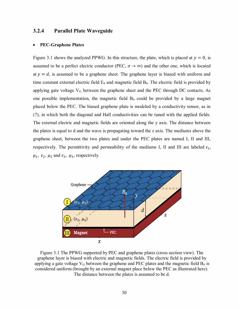
30
3.2.4 Parallel Plate Waveguide
PEC-Graphene Plates
Figure 3.1 shows the analyzed PPWG. In this structure, the plate, which is placed at , is
assumed to be a perfect electric conductor (PEC, ) and the other one, which is located
at , is assumed to be a graphene sheet. The graphene layer is biased with uniform and
time constant external electric field E0 and magnetic field B0. The electric field is provided by
applying gate voltage VG between the graphene sheet and the PEC through DC contacts. As
one possible implementation, the magnetic field B0 could be provided by a large magnet
placed below the PEC. The biased graphene plate is modeled by a conductivity tensor, as in
(7), in which both the diagonal and Hall conductivities can be tuned with the applied fields.
The external electric and magnetic fields are oriented along the y axis. The distance between
the plates is equal to d and the wave is propagating toward the z axis. The mediums above the
graphene sheet, between the two plates and under the PEC plates are named I, II and III,
respectively. The permittivity and permeability of the mediums I, II and III are labeled
, and , respectively.
Figure 3.1 The PPWG supported by PEC and graphene plates (cross section view). The
graphene layer is biased with electric and magnetic fields. The electric field is provided by
applying a gate voltage VG between the graphene and PEC plates and the magnetic field B0 is
considered uniform (brought by an external magnet place below the PEC as illustrated here).
The distance between the plates is assumed to be d.
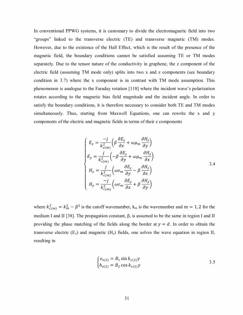
31
In conventional PPWG systems, it is customary to divide the electromagnetic field into two
“groups” linked to the transverse electric (TE) and transverse magnetic (TM) modes.
However, due to the existence of the Hall Effect, which is the result of the presence of the
magnetic field, the boundary conditions cannot be satisfied assuming TE or TM modes
separately. Due to the tensor nature of the conductivity in graphene, the z component of the
electric field (assuming TM mode only) splits into two x and z components (see boundary
condition in 3.7) where the x component is in contrast with TM mode assumption. This
phenomenon is analogue to the Faraday rotation [118] where the incident wave’s polarization
rotates according to the magnetic bias field magnitude and the incident angle. In order to
satisfy the boundary conditions, it is therefore necessary to consider both TE and TM modes
simultaneously. Thus, starting from Maxwell Equations, one can rewrite the x and y
components of the electric and magnetic fields in terms of their z components
(
)
(
)
(
)
(
)
3.4
where
is the cutoff wavenumber, km is the wavenumber and for the
medium I and II [38]. The propagation constant, β, is assumed to be the same in region I and II
providing the phase matching of the fields along the border at . In order to obtain the
transverse electric (Ez) and magnetic (Hz) fields, one solves the wave equation in region II,
resulting in
3.5
32
where and
. Also note that, the cosine part of ez(2) is set
to zero according to the fact that the electric field should vanish at the PEC surface. Also, the
sine part of hz(2) should be zero because ex(2) at the PEC border is equal to zero. Using 3.4 all
the other components of the electric and magnetic fields can be derived. The same procedure
is used to evaluate the electromagnetic fields in region I. However, in this region the ez(1) and
hz(1) should vanish while . Thus, the z components of the electric and magnetic fields in
this region are derived by solving the wave equation
3.6
Note that A1, A2, B1, B2 and β are unknowns. As the next step, the boundary conditions at y=d
is applied to the electromagnetic fields derived above. The tensor for the conductivity leads to
boundary conditions (for x and z components) expressed as
( )
(
) (
) (
) 3.7
where σd and σh are the diagonal and Hall electrical conductivities respectively from equations
(1) and (2). The top (bottom) sign of the off diagonal elements is used when the B0 field is in
the positive (negative) y direction and is related to the carrier motion. For example, the x
component of the surface current Jsx is the sum of the product of the diagonal conductivity
with ex(2) and the Hall conductivity with ez(2). Each of the boundary conditions equations 3.7
are divided in two parts (x and z components) and will results into four equations in which A1,
A2, B1, B2 and β are the unknowns. For nontrivial solution, the determinant of the two above
equations must vanish, leading to the dispersion equation which is

33
[ (
)] [ (
)]
3.8
Using the definition of and , the roots of the dispersion equation 3.8 will give the
values of βp (the propagation constant of the pth mode) as a function of the frequency. As a
first case, one could remove the magnetic bias letting the Hall conductivity vanish, , in
this equation. The PPWG therefore consists of one PEC wall and a second wall made of a few
nanometer thick finite conductivity metal. In this situation the dispersion equation will reduce
to equations (3.9) and (3.10) which represent dispersion relations for the TE and the TM
modes, respectively. The fact that the graphene conductivity can be varied by an electric field
bias provides control on the roots of these equations
(
) 3.9
(
) 3.10
The PPWG behavior can thus be continuously tuned from non-guiding if to a PEC-
PEC PPWG when . In the latter case, we get the textbook solution ⁄ (e.g.
[38]). Also, equation 3.9 is the same as (9) in [107] when (as defined in [107]).
Moreover, letting gives dispersion relations for dielectric coated conductor
waveguide [119].
To compare the graphene based PPWG with one using a normal metal, one can use the Drude
model for the conductivity needed in 3.9 and 3.10. In the case of a very thin metal layers, we
use the Drude-Smith model, which is experimentally verified in far-infrared spectral region
from 0.2 to 2.7 THz

34
(
) 3.11
where ωp, τ and c are the plasma frequency, scattering time and the fraction of the initial
carrier velocity retained after one collision, respectively [27]. For a 4 nm thick gold layer the
plasma frequency, ωp/2π, is 280 THz, scattering time, τ, is 18 fs and the fraction of the initial
carrier velocity retained after one collision, c, is -1 (full carrier backscattering) [120]. Figure
3.2 shows the real and imaginary parts of the propagation constant in PEC-graphene (for plate
separations of 100 μm, 100 nm and 10 nm) and PEC-Conductor with σ=1 s/m (for plate
separation of 100 μm) for different modes in the absence of the magnetic field. In the case of
PEC-Gold plates, due to ⁄ , ⁄ (by assuming the free space
condition for regions I and II in (3.9 and 3.10), we have ⁄ ⁄ ),
the propagation constant is approximately the same as PEC-PEC situation. Moreover,
assuming a conductor with σ=1 s/m at y=d, the results for the propagation constant are similar
to a PEC-PEC structure. Thus, for a 4 nm thick gold layer, with a minimum conductivity of
6.1×10⁵ s/m in the 0.2 to 2.7 THz frequency range, the propagation constant is almost the
same as a PEC-PEC structure.
In the case of PEC-graphene, with d=100 μm (see Fig. 3.2 (a) and (b)), although the imaginary
part of the slow-wave factor (β/k0) is almost zero for frequencies above 0.4 THz, implying low
loss propagation, the real part of the slow-wave factor (SWF) is around 1, representing a low
confinement capability of the waveguide. This is due to the fact that ⁄ √
should be greater than 1 to give fiber optic like propagation in PPWG.
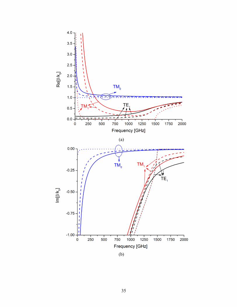
35
(a)
(b)

36
(c)
(d)
Figure 3.2 The real and imaginary parts of the propagation constant of PEC-graphene and
PEC-conductor (σ=1 s/m) PPWGs. (a) and (b) first three modes (TM0, TM1 and TE1) for the
plate separation of 100 μm (solid line: µc = 0.2 eV, dash line: µc = 0.5 eV and dots: conductor
with σ=1 s/m). (c) and (d) first mode (TM0) for the plate separation of 10 nm and 100 nm. All
in the absence of the external magnetic field .

37
Different solutions can be implemented to increase the SWF, such as increasing graphene
conductivity, using a dielectric in region II and decreasing the plate separation d. Increasing
graphene conductivity is possible by applying a stronger electric field between the graphene
and the ground plane. However, it suffers from possible current leakage under high voltage.
Inserting a dielectric material between the graphene and the ground plane makes the
waveguide behavior more similar to a dielectric image waveguide, which is not subject of this
section. However, one can investigate the properties of this waveguide based on the presented
dispersion equation in 3.8, 3.9 and 3.10. Decreasing the plate separation will shift the cutoff
frequency of TEn and TMn modes ( √ ⁄ ), but, it won’t affect the TM0 mode (here
quasi-TEM in PEC-graphene PPWG) which is the mode of interest. Therefore, in Figure 3.2,
we present the propagation constant of the PEC-graphene structure for two other plate
separations of 10 nm and 100 nm.
When there is an external magnetic field, both TE and TM modes exist simultaneously (hybrid
mode propagation). In order to calculate the phase constant of the propagating wave inside the
waveguide, we assume, for simplicity and without loss of generality, the free space condition
for both regions I and II. In this case 3.8 reduces to
[ (
)] [ (
)]
3.12
where . By solving this equation, is derived and then β can be computed.
The results are depicted in Figure 3.3 for plate separations of d=100 nm and 10 nm (for TM0
mode). The attenuation of these waveguides is presented in Table 3.2. The attenuation is
derived using where β is available from solving the dispersion equation. As
mentioned before, by increasing the separation between the plates, the imaginary part of the
propagation constant will decrease, providing a waveguide with smaller loss. But, at the same
time, it will decrease the SWF, resulting in a poor confinement of the field inside the
waveguide.
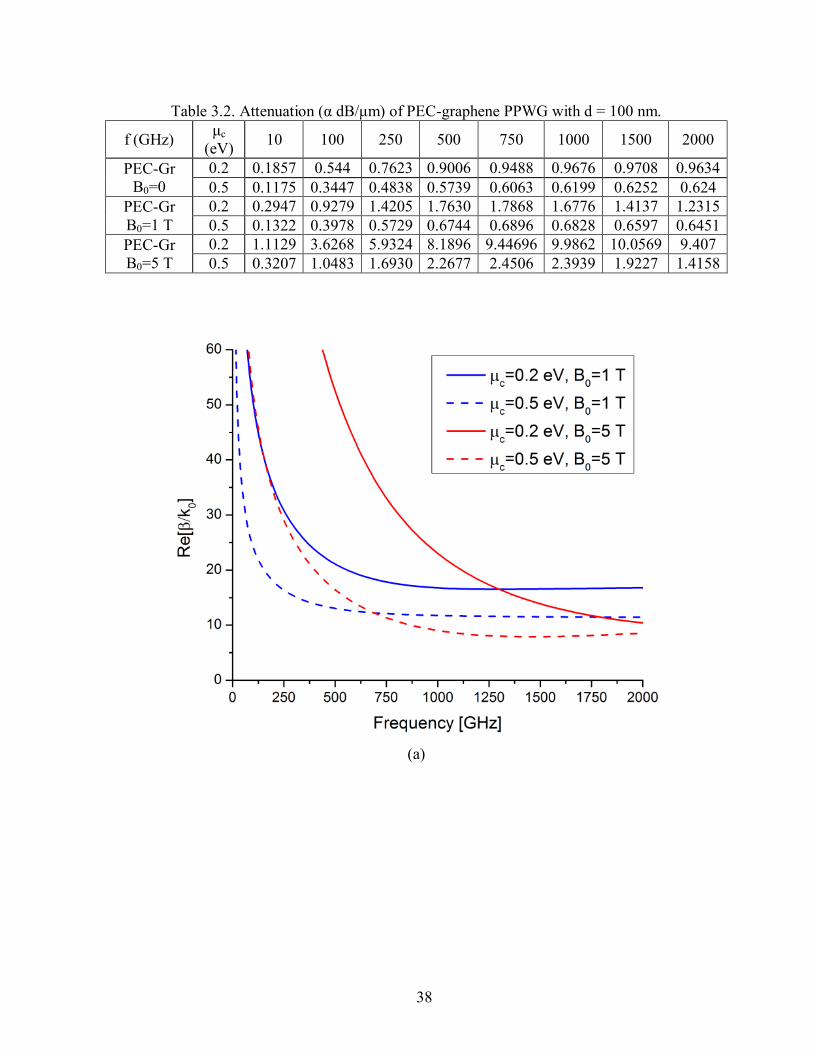
38
Table 3.2. Attenuation (α dB/μm) of PEC-graphene PPWG with d = 100 nm.
f (GHz) μc
(eV) 10 100 250 500 750 1000 1500 2000
PEC-Gr
B0=0
0.2 0.1857 0.544 0.7623 0.9006 0.9488 0.9676 0.9708 0.9634
0.5 0.1175 0.3447 0.4838 0.5739 0.6063 0.6199 0.6252 0.624
PEC-Gr
B0=1 T
0.2 0.2947 0.9279 1.4205 1.7630 1.7868 1.6776 1.4137 1.2315
0.5 0.1322 0.3978 0.5729 0.6744 0.6896 0.6828 0.6597 0.6451
PEC-Gr
B0=5 T
0.2 1.1129 3.6268 5.9324 8.1896 9.44696 9.9862 10.0569 9.407
0.5 0.3207 1.0483 1.6930 2.2677 2.4506 2.3939 1.9227 1.4158
(a)

39
(b)
(c)

40
(d)
Figure 3.3 Real and Imaginary-parts of propagation constants of PPWG with PEC-graphene
walls. These results are derived from solving equation 3.8. The graphene conductivities
derived from equations (1) and (2) assuming . The plate separations are (a), (b)
100 nm and (c), (d) 10 nm.
The time average power propagating through a surface area S is derived from the pointing
vector which can be divided in TE and TM contributions as
∫
(∑ (∬
∬
)
)
3.13

41
in which Pavg(TE) and Pavg(TM) are functions of the electric and magnetic bias fields of the
graphene. For the evaluation of the power one should find the roots of equation 3.8 and by
setting one of the unknowns in the boundary conditions, perform the integrals in 3.13.
Figure 3.4 illustrates the proportion of Pavg(TM)/Pavg(TE) for a given frequency as a function of
the chemical potential (electric bias) and magnetic bias. The blue line considers a variation of
the chemical potential from 0.05 – 0.5 eV with the magnetic field is equal to B0= 1 T. The red
line assumes a change of the magnetic field from 0 to 5 T while the chemical voltage is set to
µc=0.2 eV. The capability to control the wave propagation characteristics is evident in this
figure.
Figure 3.4 The proportion of time average power in TE and TM modes for PEC-graphene as a
function of the chemical potential (gate voltage VG) and bias magnetic field at f=100 GHz and
for d=100 nm.

42
Graphene-Graphene Plates
Let’s now consider a situation in which both plates of the PPWG are graphene sheets and are
biased with both electric and magnetic fields. This waveguide is presented in Figure 3.5,
where the upper and lower graphene layers are modeled by independent
conductivity tensor elements and
, respectively. In real experimental systems, the
graphene carrier density is known to be non-zero at zero bias. We have voluntarily omitted the
biasing scheme that would provide to each graphene film an independent voltage bias. For
sake of simplicity in the illustration we have also omitted the components generating the
spatially uniform magnetic field. Again, the same procedure as in section A is applied to
study the wave properties inside this waveguide. At first we solve the wave equation to derive
the z components of both electric and magnetic fields in medium II:
Figure 3.5 The PPWG supported by graphene plates (y-z plane). The graphene layers are
biased with electric and magnetic fields.

43
3.14
In the next step, we calculate other components of the electric and magnetic fields in this
medium. Then, the same procedure is performed in the first and third mediums. Finally, we
apply the boundary conditions at and using equation 3.7. From the electric field
boundary conditions, it is possible to describe the fields in region I and III as a function of B1,
B2, B3 and B4. Also, using the magnetic field boundary conditions at , we find that the
constants B2, B3 can be expressed in terms of B1, B4. From this and considering the boundary
conditions at , we can express the dispersion equation as
|
|
|
|
3.15
in which
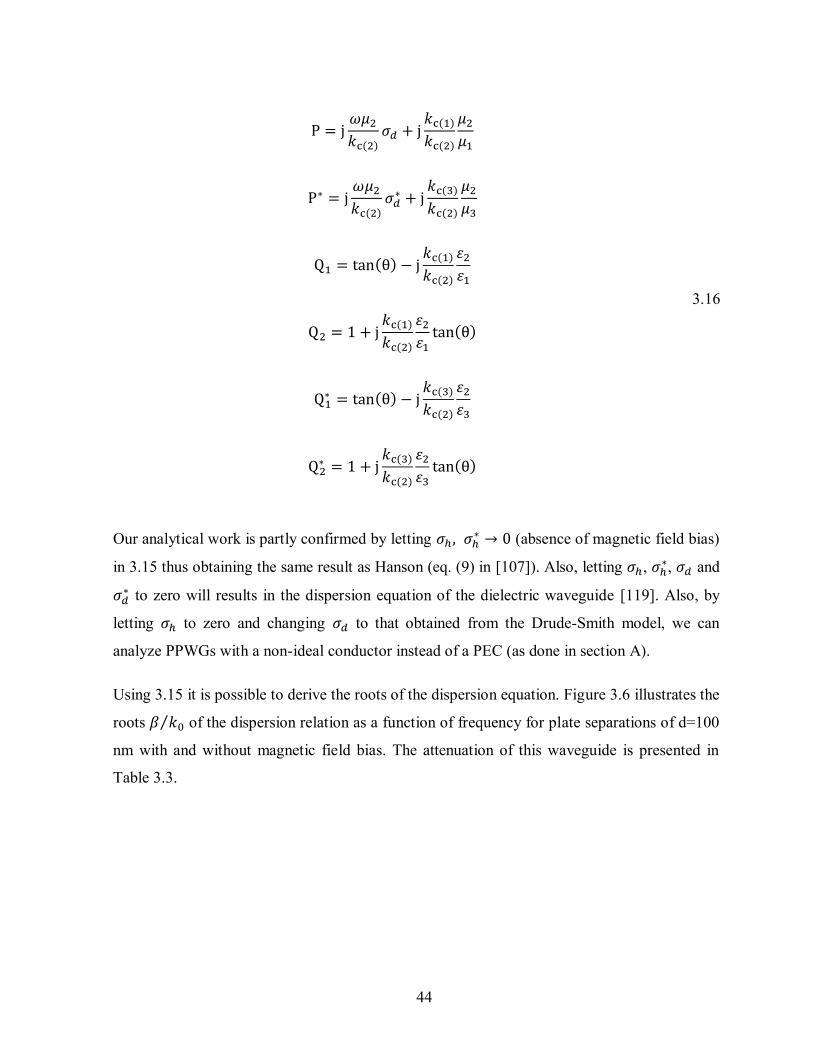
44
3.16
Our analytical work is partly confirmed by letting (absence of magnetic field bias)
in 3.15 thus obtaining the same result as Hanson (eq. (9) in [107]). Also, letting , , and
to zero will results in the dispersion equation of the dielectric waveguide [119]. Also, by
letting to zero and changing to that obtained from the Drude-Smith model, we can
analyze PPWGs with a non-ideal conductor instead of a PEC (as done in section A).
Using 3.15 it is possible to derive the roots of the dispersion equation. Figure 3.6 illustrates the
roots ⁄ of the dispersion relation as a function of frequency for plate separations of d=100
nm with and without magnetic field bias. The attenuation of this waveguide is presented in
Table 3.3.
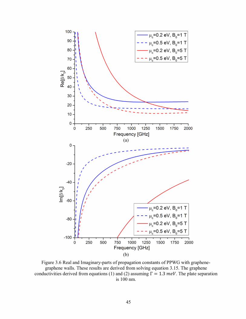
45
(a)
(b)
Figure 3.6 Real and Imaginary-parts of propagation constants of PPWG with graphene-
graphene walls. These results are derived from solving equation 3.15. The graphene
conductivities derived from equations (1) and (2) assuming . The plate separation
is 100 nm.
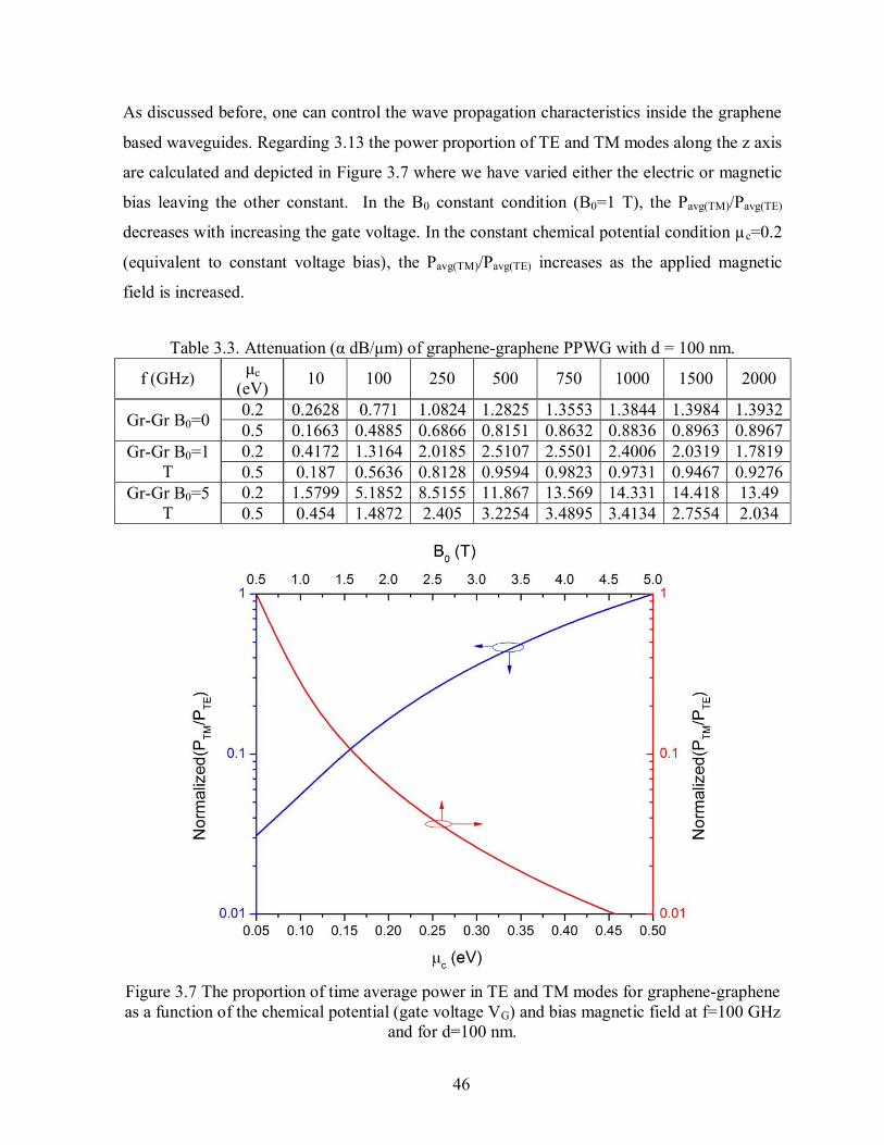
46
As discussed before, one can control the wave propagation characteristics inside the graphene
based waveguides. Regarding 3.13 the power proportion of TE and TM modes along the z axis
are calculated and depicted in Figure 3.7 where we have varied either the electric or magnetic
bias leaving the other constant. In the B0 constant condition (B0=1 T), the Pavg(TM)/Pavg(TE)
decreases with increasing the gate voltage. In the constant chemical potential condition µc=0.2
(equivalent to constant voltage bias), the Pavg(TM)/Pavg(TE) increases as the applied magnetic
field is increased.
Table 3.3. Attenuation (α dB/μm) of graphene-graphene PPWG with d = 100 nm.
f (GHz) μc
(eV) 10 100 250 500 750 1000 1500 2000
Gr-Gr B0=0 0.2 0.2628 0.771 1.0824 1.2825 1.3553 1.3844 1.3984 1.3932
0.5 0.1663 0.4885 0.6866 0.8151 0.8632 0.8836 0.8963 0.8967
Gr-Gr B0=1
T
0.2 0.4172 1.3164 2.0185 2.5107 2.5501 2.4006 2.0319 1.7819
0.5 0.187 0.5636 0.8128 0.9594 0.9823 0.9731 0.9467 0.9276
Gr-Gr B0=5
T
0.2 1.5799 5.1852 8.5155 11.867 13.569 14.331 14.418 13.49
0.5 0.454 1.4872 2.405 3.2254 3.4895 3.4134 2.7554 2.034
Figure 3.7 The proportion of time average power in TE and TM modes for graphene-graphene
as a function of the chemical potential (gate voltage VG) and bias magnetic field at f=100 GHz
and for d=100 nm.
47
3.2.5 Conclusion
We have investigated the wave propagation characteristics inside parallel plate waveguides
with either PEC-graphene or graphene-graphene plates. In the presence of a magnetic field
bias, the Maxwell equations solution inside the waveguide show that hybrid TM and TE
modes exist. We show that wave propagation characteristics can be modified by the externally
applied electric and magnetic field biases. The confinement of the field can be improved by
reducing the plate separation, increasing the permittivity of the dielectric layer or increasing
the electric bias field. The demonstrated capabilities of graphene based waveguides should
find promising applications in transmission lines, filters and antennas. To our knowledge we
are the first to report these results. The presented analytical procedure is applicable to other
guiding structures having walls with isotropic or anisotropic conductivities.

48
4 HIGH-RESISTIVITY SILICON DIELECTRIC
SLAB WAVEGUIDE
4.1 Avant-Propos
Auteurs et affiliation:
Ali Malekabadi : étudiant au doctorat, Université de Sherbrooke, Faculté de génie,
Département de génie électrique.
François Boone : professeur, Université de Sherbrooke, Faculté de génie, Département
de génie électrique.
Dominic Deslandes : professeur, Université de Québec à Montréal, Faculté de génie,
Département de génie électrique.
Denis Morris : professeur, Université de Sherbrooke, Faculté de science, Département
de génie physiques.
Serge A. Charlebois : professeur, Université de Sherbrooke, Faculté de génie,
Département de génie électrique.
Date d’acceptation: 02 april 2013
État de l’acceptation: version finale publiée
Revue: Proceedings of the International Microwave Symposium, IMS2013, June 2-7, 2013,
Seattle, USA.
Référence: [121]
Titre français: Guide d'onde THz à faibles pertes et faible dispersion en silicium haute
résistivité.
Contribution à la thèse:
Dans cet article, publié lors une conférence internationale, nous analysons un guide formé par
une couche de diélectrique d’épaisseur finie. Ce type de guide est bien connu à des fréquences
49
plus basses ou plus hautes que les fréquences térahertz et est appelé guide d’ondes en plaque
(slab waveguide). La conception est réalisée à partir de la méthode de Marcatili, qui est une
méthode approchée, mais qui donne une bonne idée du dimensions nécessaires pour les
spécifications visées. Ceci constitue alors le point de départ d'une simulation 3D
électromagnétique en utilisant le logiciel HFSS basé sur la méthode des éléments finis. La
contribution de cet article est importante: contre toute attente, ce type de guide classique, avec
une largeur conséquente, ne fonctionne pas bien en térahertz, car l'onde n'est pas assez
confinée par le diélectrique. Cette observation nous a permis de définir les conditions
géométriques optimales du guide pour obtenir un guide de type monomode sur une largeur de
fréquence optimale. Un procédé de fabrication, à la fois déconcertant au niveau de sa
simplicité et de son coût a été développé et mis en oeuvre. Le diélectrique choisi est du
silicium haute résistivité, matériau qui a l'avantage d'être compatible avec les méthodes de
fabrication des circuits microélectroniques et de présenter des pertes réduites. Afin de valider
pratiquement cette étude et ne disposant pas d'appareil de mesures de type analyseur de réseau
vectoriel autour des 1 THz, nous avons utilisé le système de spectroscopie temporel du
laboratoire du professeur Denis Morris, au département de physique. Ce système permet
d'envoyer des impulsions extrêmement courtes dans le domaine temporel, ce qui par
conséquent donne un signal à contenu fréquentiel élevé (100GHz à 3THz). Les mesures ont
permis de valider la transmission du signal térahertz dans le guide en silicium haute résistivité,
de montrer les faibles pertes de la transmission et de prouver le très bon comportement de la
vitesse de groupe conduisant à une très faible dispersion du signal. Cet article présente donc
un bon pas dans la direction afin d'obtenir un guide d'onde térahertz fonctionnel.
Résumé français :
Dans cet article, les performances des guides d'ondes constitués d'une couche de diélectrique
sont étudiées dans la région des THz. Du silicium haute résistivité (HR-Si) est choisi comme
diélectrique du fait de sa grande transparence pour les ondes THz. Un procédé de fabrication
de faible coût est proposé. L'analyse théorique repose sur l'utilisation d'un logiciel basé sur la
méthode des éléments finis en 3D (HFSS) et un système de spectroscopie THz temporel (THz-
TDS) est utilisé pour réaliser les mesures. Il est montré que le guide d'onde proposé présente
de faibles pertes et une faible dispersion.

50
Discussion:
The measurement system that we have used for the characterization of dielectric slab guides
was a THz-TDS system with the block diagram demonstrated below (Figure 1(c)). Fig. 1 (b)
shows different length HR-silicon slabs. In order to show the superiority of the proposed
structure, the THz pulses transmitted through plastic ribbon is shown in Figure 1(c) from [46].
Comparing this signal with the ones achieved in Figure 4.4, the low-loss and low-dispersive
properties of HR-silicon are obvious (less number of ripples and amplitude dropping for signal
passes through the HR-silicon wafer).
(a)
(b)
(c)
Figure 4D.1 (a) The block diagram of the THz-TDS system we used for characterization of
slab guides. (b) Photo of different lengths HR-silicon slabs. (c) THz pulses transmitted
through plastic ribbon from [46].
Laser
Optical Delay Line
Sample
PC antenna
Mirror Mirror
Detector
Amplifier
Computer

51
52
4.3 Low-loss low-dispersive high-resistivity silicon dielectric slab
waveguide for THz region
4.3.1 Abstract
In this chapter, the performance of dielectric slab waveguides in the Terahertz (THz)
frequency band is studied. High-Resistivity silicon (HR-silicon) is selected as the host material
due to its high transparency in THz region. The low-cost fabrication process of the waveguide
is described. Finite Element Method (FEM) based simulator (HFSS) and THz Time Domain
Spectroscopy (THz-TDS) system were employed to characterize the waveguide both
theoretically and experimentally. It is shown that the proposed transmission line is low-loss
and low-dispersive for a wide bandwidth.
4.3.2 Introduction
Although there is no standard definition for the Terahertz frequency band, it is generally
accepted that the band lies between microwave and infrared spectrums (mostly narrowed to
0.3 - 3 THz). THz radiations are non-ionizing and can penetrate non-metallic materials except
water [4]. Despite all difficulties in handling THz waves, they offer unique properties that can
be used in a variety of applications such as imaging, astronomy, security, medical diagnosis,
etc. [1]. Lack of efficient, compact and capable of being integrated passive and active
components are among the challenges when dealing with THz systems.
The conventional THz waveguides suffer from high losses and dispersions. The guide
attenuation is due to the ohmic losses of the metallic parts and absorption of dielectrics. In
THz frequency range, the ohmic losses are high because the surface resistance of a conductor
increase as the frequency increase ( √ ⁄ where ω is the radial frequency, μ and σ
are permeability and conductivity of the conductor, respectively) [38], [122]. The sources of
absorption in dielectrics are Drude mechanism, dielectric relaxation, and lattice vibrations
processes [3]. Dispersions in the transmitted THz wave come from the group velocity and
material characteristics (e.g. refractive index n) dependence to the frequency. According to
shortcomings of ordinary guiding structures (mainly loss and dispersion), finding a suitable
53
waveguide is a field of research attracting a lot of attention. An ideal waveguide should have
no loss, no dispersion and can be easily integrated with other components.
R. Mendis et. al, have reported an experimental and theoretical study of plastic ribbon
waveguides for THz region [46]. High-density polyethylene ribbon was used to conduct the
THz wave. They had incorporated the THz-TDS setup to perform the measurements. They
observed a dispersive and low-loss characteristics in THz band [46]. Although, they didn't talk
about the source of dispersion, we believe that this dispersive behaviour is from the frequency
dependence characteristics (basically in refractive index) of the high-density polyethylene
used for the guide. This dispersive behaviour of the guide is deeply studied in [51].
Here, HR-silicon dielectric slab waveguide is studied in the THz band. HR-silicon was chosen
due to its high transparency in the THz region [69]. In section 4.3, theory and analysis with
FEM based simulator (HFSS) is presented. Then, in section 4.4, the low-cost fabrication
process of the waveguide is described. Section 4.5 deals with Time Domain Spectroscopy
(THz-TDS) system that was employed to characterize the waveguide experimentally.
4.3.3 Theory and Analysis
Figure 4.1 shows the geometry of the dielectric waveguide. The thickness of the waveguide is
d. The width and length of the slab are variables. Relative permittivity and permeability are εr1
and μr1, respectively. In dielectric slabs, unlike the metallic guides, the cutoff frequency is
defined as there is no attenuation above [119]. Considering an ideal dielectric this attenuation
must be counted for the radiation from the dielectric slab. The cutoff frequency (the lowest
frequency for unattenuated propagation) can then be computed by
√ ⁄ where n = 0, 1, 2, ... for both TEn and TMn modes [119]. One can
note that, the cutoff frequency of TM0 and TE0 is zero. Here, we only consider TM modes
with electric field polarized along the x-direction as provided by the photoconductive antenna.

54
Figure 4.1 The dielectric slab waveguide geometry. The wave propagates toward the z
direction. The THz signal will illuminate the side wall of the slab shown by the hatched
circular area.
As shown in Figure 4.1, the THz signal that comes from the photoconductive antenna will
illuminate a circular area on the edge of the silicon slab. The diameter of this circle is
estimated to be 200 μm. When the THz signal enters the silicon slab, the beamwidth starts to
expand. Since the propagated signal is collected on the other side of the waveguide by a set of
parabolic mirrors from a spot of the size as for the entry (see Figure 4.2(b)), the propagating
waves toward the sides will be a source of loss. This phenomenon is depicted in Figure 4.3 by
using HFSS for two waveguides with different widths (ω = 250 μm and ω = 1 mm). The
difference between the transmissions S-parameters is due to different return losses and THz
beam broadening loss. By decreasing the slab width to the order of the illumination spot, this
broadening loss minimized.
4.3.4 Fabrication and Measurement
Different silicon slab waveguides were made by means of microelectromechanical system
(MEMS) fabrication techniques. We used (100) orientation 3 inches HR-silicon (ρ > 1 × 10³
Ωcm) wafers with a thickness of 380 μm. Initially, the wafers were coated with a 14 μm
photoresist (AZ9245) layer. This layer acts as a mask during the etching process and should be
thick enough to survive this period. This resist layer was then patterned by conventional
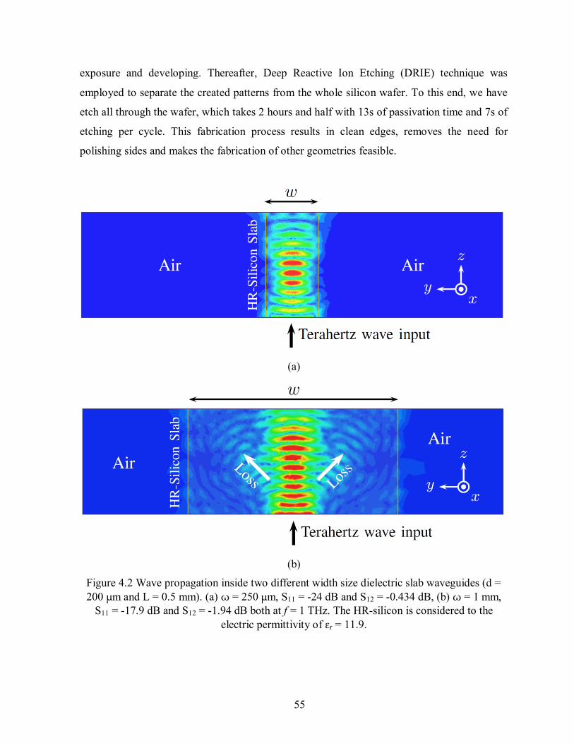
55
exposure and developing. Thereafter, Deep Reactive Ion Etching (DRIE) technique was
employed to separate the created patterns from the whole silicon wafer. To this end, we have
etch all through the wafer, which takes 2 hours and half with 13s of passivation time and 7s of
etching per cycle. This fabrication process results in clean edges, removes the need for
polishing sides and makes the fabrication of other geometries feasible.
(a)
(b)
Figure 4.2 Wave propagation inside two different width size dielectric slab waveguides (d =
200 μm and L = 0.5 mm). (a) ω = 250 μm, S11 = -24 dB and S12 = -0.434 dB, (b) ω = 1 mm,
S11 = -17.9 dB and S12 = -1.94 dB both at f = 1 THz. The HR-silicon is considered to the
electric permittivity of εr = 11.9.

56
A THz Time-Domain Spectroscopy (THz-TDS) system was then employed to characterize the
waveguide performance. The THz pulses were generated by a photoconductive antenna. This
antenna was excited by a 60 fs mode-locked Ti-sapphire oscillator. Thereafter, the THz pulse
were collected by a hemispherical silicon lens on the emitter antenna and focused on the
sample by means of a pair of off-axis parabolic mirrors. Another pair of mirrors employed to
collect and focus the THz signal passing through the waveguide on the detector.
In order to couple the THz signal into the waveguide, one can use plano-cylindrical silicon
lenses (shown in Figure 4.4 (c)). These lenses will concentrate the THz signal into the
waveguide. However, by using such silicon lenses, we will add four other air-silicon interfaces
which introduce the reflections. Also, the THz signal that travels inside the waveguide will
meet the silicon air interfaces on the top and bottom walls with a small incident angle (which
could be less than the critical angle). Therefore, the condition for total internal reflection is not
satisfied leading to losses by refracted signal. By coupling the signal directly from the mirror
to the waveguide, we will eliminate the reflections in the air-silicon interfaces and increase the
incident angle on the walls (see Figure 4.4 (b)). Here, in the following measurements we have
coupled the THz signal directly into the dielectric waveguide.
(a)
57
(b)
(c)
Figure 4.3 (a) measurement setup. (b) and (c) demonstration of THz wave meeting the air-
silicon interface. By introducing plano-cylindrical lens, the incident angle θi will decrease
result in poor confinement of THz wave.
Figure 4.5 and 4.6 show the four measured signals in both time and frequency domains,
respectively. The first signal (reference I) is obtained while the THz wave is travelling through
the air between two mirrors (as illustrated in Figure 4.4(a) without absorbers and waveguide).
The second signal (reference II) is measured while two absorbers are installed (again without
waveguide). These absorbers are used to suppress the THz propagation outside of the silicon
slab and prevent surface waves. The third and fourth traces are the transmitted signals inside
the high-resistivity silicon slabs with L = 5 mm and L = 10 mm, respectively.
The THz signal is delayed by 40.5 ps in the case of L = 5 mm because the wave group velocity
is smaller that the speed of light. In the case of L = 10 mm silicon slab this delay is around two
times that of the previous one and equal to 78 ps. The small secondary pulses are due to
reflections in measurement setup. Looking at the pulses in time domain, one can observe the
low-dispersion characteristic of the waveguide as there are no extra ripples and it is not
stretched in time.

58
Figure 4.4 THz pulses transmitted through the air and silicon waveguides. From bottom to top
travelled in: air, air with absorbers, silicon waveguide with L = 5 mm and L = 10 mm (see
Figure 4.4). The width of the waveguide is w = 15 mm for both cases. The baselines of the
pulses have been offset for clarity.
Figure 4.5 Measured transmission spectra of reference and transmitted THz signals. From top
to bottom travelled in: air, air in the presence of the absorbers, silicon waveguide with L = 5
mm and L = 10 mm. The width of the waveguide is w = 15 mm for both cases.
59
4.3.5 Conclusion
We have presented a low-loss low-dispersive dielectric waveguide suitable for THz frequency
range. HR-silicon is the host material due to its high transparency in THz band. The low-cost
fabrication process is described. FEM based simulator (HFSS) and THz Time Domain
Spectroscopy (THz-TDS) system were employed to characterize the waveguide theoretically
and experimentally, respectively. The time-domain and frequency-domain measured signals
proofing the low-loss and low-dispersion properties of the HR-dielectric slabs.

60
5 SILICON DIELECTRIC RIBBON WAVEGUIDE
5.1 Avant-Propos
Auteurs et affiliation:
Ali Malekabadi : étudiant au doctorat, Université de Sherbrooke, Faculté de génie,
Département de génie électrique.
Serge A. Charlebois : professeur, Université de Sherbrooke, Faculté de génie,
Département de génie électrique.
Dominic Deslandes : professeur, Université de Québec à Montréal, Faculté de génie,
Département de génie électrique.
François Boone : professeur, Université de Sherbrooke, Faculté de génie, Département
de génie électrique.
Date d’acceptation: Le 23 avril 2014
État de l’acceptation: acceptée
Revue: IEEE Transaction on Terahertz Science and Technology
Référence: [123]
Titre français: Guide d'onde monomode à faibles pertes à base de silicium haute résistivité
pour la propagation dans les bandes F et G.
Contribution à la thèse:
Dans cet article, l'étude précédente est affinée et poussée d'une étape. Cette fois-ci, un
véritable guide d'onde optimisé géométriquement est réalisé, ainsi qu'un système de couplage
afin de pouvoir exciter ce guide dans le domaine fréquentiel, et donc d'utiliser un analyseur de
réseau vectoriel, outil de mesure fondamental dans le domaine de l'électronique haute
fréquence. Pour ce faire, et afin de pouvoir utiliser les capacités de mesure du regroupement
stratégique CREER, nous avons sélectionné deux bandes de fréquences, soit la bande F (90 à
140GHz) et la bande G (140 à 220GHz), sans faire de compromis sur la théorie générale et le

61
processus de réalisation. Ceci implique donc que ces mesures et ces réalisations peuvent être
transposées en fréquence, et atteindre la véritable bande térahertz au-dessus de 300GHz.
Plusieurs aspects très novateurs et intéressants ont été découverts. Cependant, l'article ne
présente que les résultats de base puisque les résultats importants doivent être valorisés à
travers le dépôt de brevets. Principalement, cet article démontre clairement qu'un guide d'onde
constitué d'une tige à section carrée de silicium haute résistivité est une solution élégante et
pérenne pour guider les ondes térahertz. Les mesures de la constante de propagation viennent
confirmer de façon éclatante la validité du concept. L'évaluation des pertes est faite en
distinguant les pertes par diélectrique et les pertes par rayonnement. Les pertes maximales sont
de 0.087dB/cm ce qui rend ce type de guide comparable à d'autres solutions déjà étudiées par
d'autres chercheurs et résumées dans un tableau de cet article. Un des avantages de la solution
proposée, et certainement pas le moindre, réside dans la facilité du processus de réalisation, sa
fiabilité et sa répétabilité ainsi que dans la compatibilité avec la technologie CMOS,
technologie dominante dans la microélectronique. Au niveau des paramètres de diffractions
(S), paramètres de caractérisation classique dans le domaine fréquentiel, les résultats de
mesures et de simulation sont concordants, particulièrement pour la bande F. Pour la bande G,
les résultats semblent moins bons pour la transmission alors que pour la réflexion, les résultats
confirment la simulation. Une telle divergence sur les résultats de mesures indique un
problème dans les mesures elles-mêmes, problème compréhensible du fait des fréquences
utilisées. Effectivement, dans la bande G, le port d'excitation du guide est un guide d'onde
WR-5 dont les dimensions internes sont 1,2954mm par 0,6477mm exigeant un alignement de
grande précision, plus ou moins bien obtenu par la fixture de test développée sur mesure
puisqu'aucun standard et solution connue n'existent à ces fréquences. Pour conclure, cet article
pose les bases d'une nouvelle ligne de transmission, simple de réalisation, à faible coût,
pouvant fonctionner dans la bande des térahertz. Ceci représente un jalon important, car de
nombreux composants, comme des filtres, des coupleurs, des diviseurs ou combineurs de
puissance, des réseaux d'alimentation d'antennes sont tous réalisés à base de ligne de
transmission.
Résumé français :

62
Dans cet article, différents guides d'ondes constitués d'une tige de diélectrique sont conçus
pour fonctionner dans les bandes de fréquence F (90-140 GHz) et G (140-220 GHz) et sont
caractérisés par des mesures. Du silicium haute résistivité (HR-Si) est utilisé du fait de sa
transparence à ces fréquences et un procédé de fabrication à faible coût est présenté pour
réaliser ces guides. La propagation des modes dans ce type de guide est analysée en utilisant la
méthode proposée par Marcatili d'une part et par la méthode multiligne d'autre part. Une
procédure de conception pour optimiser la propagation monomode est proposée. L'atténuation
de l'onde dans le guide est discutée. Nos mesures montrent que ce type de guide, en silicium
haute résistivité, a des pertes inférieures à 0.087dB/cm (0.01 cm-1
) pour toute la plage de
fréquence considérée. Ces guides ont été réalisés en utilisant des méthodes de microfabrication
et les mesures correspondent de façon convenable aux simulations théoriques réalisées.
Discussion:
Table 5.1 of this chapter summarizes the key characteristics of dielectric waveguides already
published in the literature. Our proposed structure is within the solid-core category with air-
clad and has attenuation of less than 0.057 dB/cm over the bandwidth of 0.09-0.22 THz. The
propagating modes inside the structure are depicted in Figure 5D.1. One should note that the
Ey12 and Ey21 have different cutoff frequencies and thus they are not degenerated modes.
Figure 5 5D.1 Electric field distribution of the first four modes inside DRW with .
The radiation losses in Figure 5.5 are computed by subtracting the losses of DRW when
simulated with the finite silicon conductivity from the simulation in which silicon is treated a
perfect lossless dielectric. In the other words, it is assumed that the sources of losses other than
the silicon resistivity are radiation losses. We derived the S-parameters (to calculate the loss
coefficients) from the simulations in which the DRW is excited through transitions to
rectangular waveguides. These transitions are well-performing only after 105 GHz in the F
band and after 170 GHz in the G band. Therefore, the radiation losses demonstrated in

63
Figure 5.5 implies that the electromagnetic fields are fully confined inside the waveguide. One
should note that the main reason that we couldn’t derive the attenuation constant from VNA
measurements was the fact that the errors of the machine were higher than the value of the
attenuation.
64
5.2 High-resistivity silicon dielectric ribbon waveguide for single-
mode low-loss propagation at F/G-bands
5.2.1 Abstract
In this chapter, Dielectric Ribbon Waveguides (DRWs) are designed and characterized to
work in the F (90-140 GHz) and G (140-220 GHz) frequency bands. High resistivity silicon
(HR-silicon), due to its high transparency in these bands, and a low-cost fabrication process
were selected for the fabrication of these waveguides. The guided modes of DRW are studied
using Marcatili and multi-line methods. A design procedure for optimal single-mode
propagation was introduced. The wave attenuation inside the waveguide is discussed. Our
experiments show that HR-silicon DRW has less than 0.087 dB/cm (0.01 cm-1
) of loss over
the guiding bandwidth. The designed DRWs were realized using microfabrication techniques.
The measurements are in very good agreement with theoretical predictions.
5.2.2 Introduction
Like its adjacent frequency bands, Terahertz (THz) is non-ionizing [124]. It can penetrate non-
metallic materials but is attenuated drastically in the presence of water or water vapor [124]. It
is also known that the THz radiation is unharmful [125] giving way to a wide variety of
applications in space, spectroscopy, imaging, medical and communication [3], [126].
Waveguides are the core elements of THz circuits. Ideal waveguides neither have propagation
loss nor dispersion. Furthermore, they enable realisation of other passive components such as
filters, couplers and antennas. THz guides are normally inspired from two worlds: microwave
waveguides and optical fibers. Classic metallic microwave waveguides (e.g. parallel plate
waveguide [30], [35], rectangular/circular waveguides [24], bare metal wires [127] and etc.)
normally have high propagation losses due to the ohmic losses in metallic parts. Some
modifications on these structures have allowed reaching lower levels of attenuation (e.g. [20],
[128], [129]). For example in [20], the transmission losses of the hollow metallic waveguide
are reduced by coating the inner metallic surface with a thin dielectric layer (typically 10-20
μm). The goal was to keep the propagating wave (energy) far from the metallic side walls.
65
Dielectric waveguides are derived from optical fibers. They can be divided into hollow-core
[33], [44], [45], solid-core [46]–[51], [130], [131] and porous-core [52]–[54] categories as
suggested by [43]. In hollow-core waveguides the guiding mechanism is either total reflection
from dielectric with imaginary refractive index (for specific frequency band) [44],
antiresonance [33] or formation of photonic bandgap [45]. Solid core waveguides have air
(e.g. [46]) or photonic crystal clads (e.g. [48]) where the guiding mechanism is based on total
internal reflection. These waveguides suffer from high propagation losses due to dielectric
absorption. In this class of waveguides finding a low-loss and low dispersive material is the
key issue. In the porous-core group (fibers with subwavelength air holes) the guiding
mechanism is again total internal reflection [52]. The holes are made in order to improve the
absorption loss (simply by increasing wave propagation in air) and wave confinement. Table
5.1 summarize the key characteristics of dielectric waveguides.
Although the losses of hollow-core structures are generally lower, in this chapter, we will
focus on solid-core dielectric waveguides (since they are easier and cheaper to fabricate) and
will address both loss and dispersion problems. Solid-core waveguides were proposed for
millimetre and submillimetre band in [49], [50] where, from theoretically point of view, much
less losses than microstrip lines, coplanar waveguide and even hollow-core metallic
waveguides like rectangular ones are expected. The 10:1 aspect ratio ribbon was made of
ceramic alumina and showed an attenuation factor of 10 dB/km in the 30-40 GHz frequency
band. Authors predicted higher frequency applications for their ceramic waveguide but their
experimental results were limited to 30-40 GHz band.
R. Mendis et. al, have reported an experimental and theoretical study of plastic ribbon
waveguides for THz region [46]. High-density polyethylene ribbon were used to conduct the
THz wave. They have used the THz Time Domain Spectroscopy (THz-TDS) technique to
perform the measurements. They observed a dispersive and low-loss characteristic in THz
band [46]. However, they didn't investigate the source of dispersion but in [51] they point to
the portions of the transmitted energy inside and outside of the waveguide. Using solid-core
structures other passive components like phase shifters [130] and switches [131] were also
realized.
66
As mentioned earlier, finding a highly transparent material in THz region is the most crucial
part of solid core dielectric waveguide design. In [69], it is shown that the HR-silicon is one of
the potential candidates since its absorption coefficient is estimated to be less than 0.087
dB/cm (0.01 cm-1
) over the entire range of 0.1-1 THz. Also, the index of refraction varies only
by 0.0001 over this frequency range [69] which suggests very low dispersion properties of the
HR-silicon. This low dispersion characteristic is experimentally demonstrated in our previous
work with a HR-silicon slab waveguide characterized using THz-TDS system [121].
In this chapter, we design and characterize 1:1 dielectric ribbon waveguides made of HR-
silicon for F and G bands. This 1:1 geometry favors mono mode propagation by comparison to
work of other authors. HR-Silicon was selected due to its high transparency in the THz region.
In section 5.3, a modal analysis is performed by employing Marcatili [132] and multi-line
[133] methods. This discussion leads to a design procedure to acquire optimal single mode
propagation bandwidth. The designed waveguides are also simulated using Finite Element
Method (FEM) based software (HFSS). A low-cost fabrication process is described in section
5.4 using Deep Reactive Ion etching (DRIE) techniques. A comparison between simulated and
measured results is presented.

67
Table 5.1. Some key characteristics of dielectric waveguides
Guiding Mechanism Disadvantage Advantage Materia
l α [dB/cm] f [THz] Ref.
Hollow
-core
Total reflection
(dielectric with εr < 0
for specific band)
Large Size
Narrow band
Multi-mode propagation
Low loss
Low dispersion
PVDF (avg.)
0.074 1 – 2 [44]
Antiresonance Teflon ~ 0.1737 0.35 – 0.55 [33]
Photonic bandgap
Large size
Narrow band
Scattering loss
Confinement loss
Low loss
Low dispersion
Teflon
HDPE
< 0.05
< 0.01
0.9 – 1.15
0.85 - 1 [45]
Solid-
core
Total
internal
reflection
Air-clad Absorption loss
High bend loss
Lower loss(a)
Subwavelentgh dimensions
(flexible)
Wider bandwidth(b)
HDPE
PE
---
< 0.087
0.1 – 2.5
0.31 – 0.35
[46]
[47]
Photonic
crystal-
clad
Absorption loss
Scattering loss
Lower loss(a)
Wider bandwidth(b)
HDPE < 4.34 0.1 – 3 [48]
Porous
-core
Total internal
reflection Fabrication complexity
Better field confinement(c)
Lower loss(c)
Lower dispersion(c)
PE
PE
= 0.087
< 0.7
0.3
0.2 – 0.35
[131]
[52]
(a) generally; in comparison with hollow-core metallic waveguides, coplanar waveguides and microstrip transmission lines. The losses
of these waveguides are higher than the parallel plate metallic waveguides, bare metal wire and dielectric coated hollow-core
waveguides. (b)
generally; in comparison with hollow-core (air-core) waveguides because the guiding mechanism is total internal reflection. (c)
generally; in comparison with solid-core guides.

68
5.2.3 Theory and analysis
In this section, we use Marcatili’s method as starting point to study the propagative modes in
solid-core dielectric waveguides in order to find a geometry allowing monomode propagation.
Then HFSS software is used to simulate the real structure from which propagation constants
and losses are evaluated.
Modal Analysis
A perspective view of the rectangular DRW is shown in Figure 5.1(a). The structural
dimensions of the rectangular DRW is a and b along x and y axes. The permittivity and
permeability of the waveguide ε1 and μ1, respectively. Here, two methods are employed to
obtain the propagation constants of the rectangular DRW. Initially, an approximate method
presented by Marcatili [132] is used. The environment surrounding the rectangular DRW is
delimited into considered and omitted (shaded) regions. The boundary conditions along the
edges of the shaded regions are ignored (see Figure 5.1(b)). This assumption was made
knowing that most of the guided power is maintained inside the core region (region 1) due to
high dielectric contrast (εr(silicon) = 11.9).
(a)
(b)
Figure 5.2 (a) Perspective view of the DRW and coordinate system (b) Cross-section of the
guide and ignored boundary condition (in red) and regions (shaded) in Marcatili method.
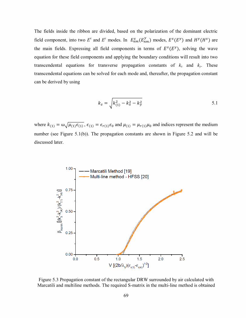
69
The fields inside the ribbon are divided, based on the polarization of the dominant electric
field component, into two Ex and E
y modes. In
modes, and are
the main fields. Expressing all field components in terms of , solving the wave
equation for these field components and applying the boundary conditions will result into two
transcendental equations for transverse propagation constants of kx and ky. These
transcendental equations can be solved for each mode and, thereafter, the propagation constant
can be derived by using
√
5.1
where √ , and and indices represent the medium
number (see Figure 5.1(b)). The propagation constants are shown in Figure 5.2 and will be
discussed later.
Figure 5.3 Propagation constant of the rectangular DRW surrounded by air calculated with
Marcatili and multiline methods. The required S-matrix in the multi-line method is obtained
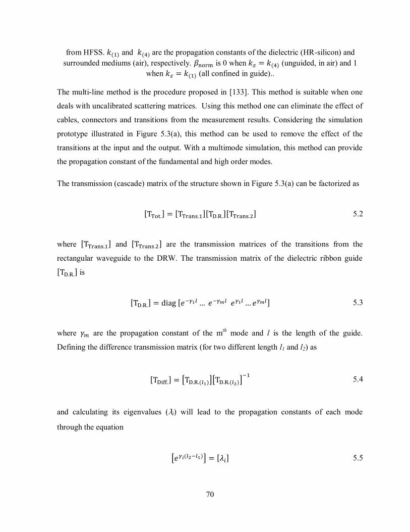
70
from HFSS. and are the propagation constants of the dielectric (HR-silicon) and
surrounded mediums (air), respectively. is 0 when (unguided, in air) and 1
when (all confined in guide)..
The multi-line method is the procedure proposed in [133]. This method is suitable when one
deals with uncalibrated scattering matrices. Using this method one can eliminate the effect of
cables, connectors and transitions from the measurement results. Considering the simulation
prototype illustrated in Figure 5.3(a), this method can be used to remove the effect of the
transitions at the input and the output. With a multimode simulation, this method can provide
the propagation constant of the fundamental and high order modes.
The transmission (cascade) matrix of the structure shown in Figure 5.3(a) can be factorized as
[ ] [ ][ ][ ] 5.2
where [ ] and [ ] are the transmission matrices of the transitions from the
rectangular waveguide to the DRW. The transmission matrix of the dielectric ribbon guide
[ ] is
[ ] [ ] 5.3
where are the propagation constant of the mth
mode and l is the length of the guide.
Defining the difference transmission matrix (for two different length l1 and l2) as
[ ] [ ][
]
5.4
and calculating its eigenvalues (λi) will lead to the propagation constants of each mode
through the equation
[ ] [ ] 5.5

71
Here, the S-parameters of two different length waveguides were simulated with HFSS. Figure
5.3(a) illustrates the simulation geometry consisting of two DRW to rectangular waveguide
transitions. The coupling mechanism and electric field propagation is shown in Figure 5.3(b).
The normalized propagation constant ( (
) (
)) of the waveguide
[132], calculated with the above methods, are plotted in Figure 5.2. This normalized
propagation constant varies between 0 and 1. It is 0 when (unguided, in air) and 1
when (all confined in guide). A very good agreement between the two methods is
observed.
(a)
(b)
Figure 5.4 (a) Perspective view of the DRW and coordinate system (b) Cross-section of the
guide and ignored boundary condition (in red) and regions (shaded) in Marcatili method.
72
Waveguide design
In a DRW, unlike in a rectangular waveguide,
or
modes can't exist. Therefore,
and
modes are the first and second modes, respectively. Considering the first two modes
and assuming that the wave is completely confined inside the dielectric and taking we
have
√
√
√
√
5.6
where is the cut-off radial frequency of the nth
mode and is the phase velocity inside
the DRW. Also, for the case we have
√
√
5.7
It is clear that the bandwidth of single mode propagation is larger for
the case . Figure 5.4 shows the propagation constant of dielectric waveguide for
different ratios using Marcatili method. It confirms that the optimal single mode
propagation can be achieved for . A small difference between single mode propagation
bandwidth derived from Marcatili method (Figure 5.4) and from eq. 5.6 and 5.7 is due to
assumption of complete wave confinement in the dielectric in the latter case (like in
rectangular waveguide).
DRWs are normally excited through a taper transition to rectangular waveguides. Extensive
simulations demonstrate a very good matching can be achieved by selecting
where is the height of the rectangular waveguide. In the case of the F (WR-8) and G

73
(WR-5.1) bands this height is 1.016 mm and 0.6477 mm, respectively. Here, we used
HR-silicon wafers with thickness of 585 μm and 385 μm for the F and G bands, respectively.
In order to simplify fabrication process, the HR-silicon wafers were chosen with a thickness
equal to the desired DRW height .
(a)
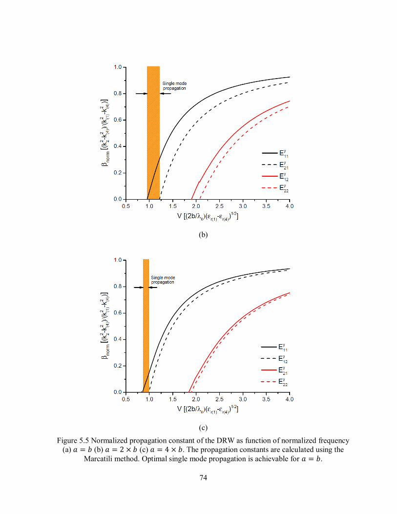
74
(b)
(c)
Figure 5.5 Normalized propagation constant of the DRW as function of normalized frequency
(a) (b) (c) . The propagation constants are calculated using the
Marcatili method. Optimal single mode propagation is achievable for .

75
Waveguide attenuation
The DRW attenuation comes from dielectric and radiation losses. Using the multi-line method
one can calculate the attenuation constant as well as the propagation constant. By assuming a
lossless dielectric, one can calculate the attenuation due to the radiations from the DRW walls
( ). Then, using the finite conductivity of the HR-silicon, simulations give the total losses
. The dielectric losses ( ) are obtained from the difference between these results.
Figure 5.5 shows the total losses and the dielectric and radiation contributions. One can
observe that the attenuation of the DRW is mainly due to the dielectric loss. The total loss of
the DRW is less than 0.087 dB/cm (0.01 cm-1
) in both bands (which was estimated in [69]),
representing the low-loss characteristics of the proposed HR-silicon DRW.
Figure 5.6 Normalized propagation constant of the DRW as function of normalized frequency
(a) (b) (c) . The propagation constants are calculated using the
Marcatili method. Optimal single mode propagation is achievable for .
Waveguide bend
76
In DRWs the propagating wave tends to radiate at the bends. The radiating power from a
bended guide (bend loss) can be defined in terms of S-parameters as
| | | |
5.8
This equation (5.8) represents a normalized power-balance equation, and PRad is then
expressed in dB.
Figure 5.6 demonstrates the radiated power as a function of bend radius. The structure is
depicted in the inset of the figure. For comparison, the PRad have been calculated and reported
in Figure 5.6 for two straight lines with lengths equal to the length of the bends. The dielectric
losses of the silicon are neglected in order to obtain only the radiated power from the bend
curvature and the lines. It is obvious that by increasing the radius, the bend curve sharpness
decreases which reduces the radiation. For a radius greater than 3.5mm the bend radiations
converge and are very close to the ones of a straight line of the same length, which shows that
the radiated power is very low.
5.2.4 Fabrication and measurement
One of the advantages of making DRWs from HR-silicon is its compatibility with micro-
fabrication techniques. Two 585 μm and 385 μm thickness HR-silicon wafers with a resistivity
of Ωcm and Ωcm, were used for F and G bands respectively.
Conventional photolithography techniques were used to create the DRW patterns. Afterwards,
Deep Reactive Ion Etching (DRIE) was employed to etch through the silicon wafers. Both
lithography and etching steps were tailored for two wafer thicknesses. A tether lattice is
designed to hold the DRW in the center of rectangular waveguide. Also, the DRW is
suspended in air by this tether lattice above a wide groove in the support and any contact
between DRW and the metallic support is avoided. Simulations show that, electromagnetic
waves cannot propagate inside the holding arms since the observed input impedance from
these lines are very high.
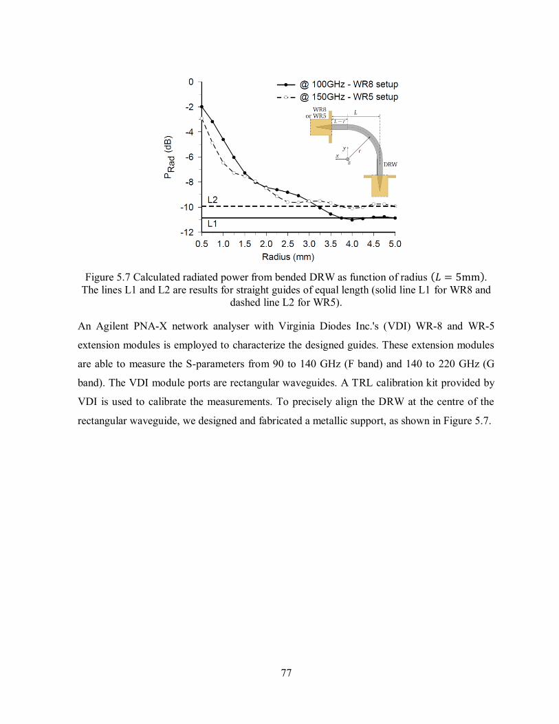
77
Figure 5.7 Calculated radiated power from bended DRW as function of radius . The lines L1 and L2 are results for straight guides of equal length (solid line L1 for WR8 and
dashed line L2 for WR5).
An Agilent PNA-X network analyser with Virginia Diodes Inc.'s (VDI) WR-8 and WR-5
extension modules is employed to characterize the designed guides. These extension modules
are able to measure the S-parameters from 90 to 140 GHz (F band) and 140 to 220 GHz (G
band). The VDI module ports are rectangular waveguides. A TRL calibration kit provided by
VDI is used to calibrate the measurements. To precisely align the DRW at the centre of the
rectangular waveguide, we designed and fabricated a metallic support, as shown in Figure 5.7.
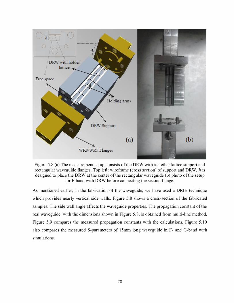
78
Figure 5.8 (a) The measurement setup consists of the DRW with its tether lattice support and
rectangular waveguide flanges. Top left: wireframe (cross section) of support and DRW, h is
designed to place the DRW at the center of the rectangular waveguide (b) photo of the setup
for F-band with DRW before connecting the second flange.
As mentioned earlier, in the fabrication of the waveguide, we have used a DRIE technique
which provides nearly vertical side walls. Figure 5.8 shows a cross-section of the fabricated
samples. The side wall angle affects the waveguide properties. The propagation constant of the
real waveguide, with the dimensions shown in Figure 5.8, is obtained from multi-line method.
Figure 5.9 compares the measured propagation constants with the calculations. Figure 5.10
also compares the measured S-parameters of 15mm long waveguide in F- and G-band with
simulations.
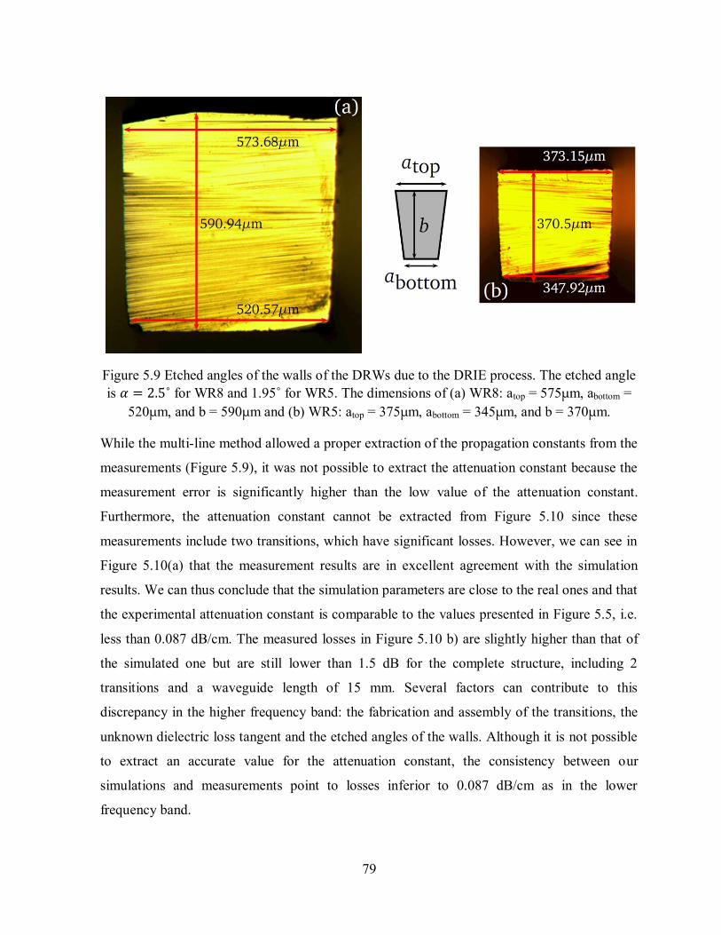
79
Figure 5.9 Etched angles of the walls of the DRWs due to the DRIE process. The etched angle
is ˚ for WR8 and 1.95˚ for WR5. The dimensions of (a) WR8: atop = 575μm, abottom =
520μm, and b = 590μm and (b) WR5: atop = 375μm, abottom = 345μm, and b = 370μm.
While the multi-line method allowed a proper extraction of the propagation constants from the
measurements (Figure 5.9), it was not possible to extract the attenuation constant because the
measurement error is significantly higher than the low value of the attenuation constant.
Furthermore, the attenuation constant cannot be extracted from Figure 5.10 since these
measurements include two transitions, which have significant losses. However, we can see in
Figure 5.10(a) that the measurement results are in excellent agreement with the simulation
results. We can thus conclude that the simulation parameters are close to the real ones and that
the experimental attenuation constant is comparable to the values presented in Figure 5.5, i.e.
less than 0.087 dB/cm. The measured losses in Figure 5.10 b) are slightly higher than that of
the simulated one but are still lower than 1.5 dB for the complete structure, including 2
transitions and a waveguide length of 15 mm. Several factors can contribute to this
discrepancy in the higher frequency band: the fabrication and assembly of the transitions, the
unknown dielectric loss tangent and the etched angles of the walls. Although it is not possible
to extract an accurate value for the attenuation constant, the consistency between our
simulations and measurements point to losses inferior to 0.087 dB/cm as in the lower
frequency band.
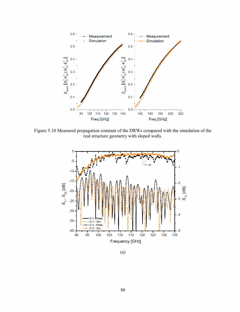
80
Figure 5.10 Measured propagation constant of the DRWs compared with the simulation of the
real structure geometry with sloped walls.
(a)
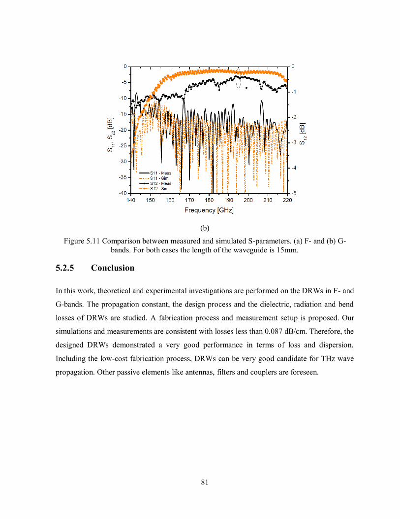
81
(b)
Figure 5.11 Comparison between measured and simulated S-parameters. (a) F- and (b) G-
bands. For both cases the length of the waveguide is 15mm.
5.2.5 Conclusion
In this work, theoretical and experimental investigations are performed on the DRWs in F- and
G-bands. The propagation constant, the design process and the dielectric, radiation and bend
losses of DRWs are studied. A fabrication process and measurement setup is proposed. Our
simulations and measurements are consistent with losses less than 0.087 dB/cm. Therefore, the
designed DRWs demonstrated a very good performance in terms of loss and dispersion.
Including the low-cost fabrication process, DRWs can be very good candidate for THz wave
propagation. Other passive elements like antennas, filters and couplers are foreseen.
82
6 BANDPASS FILTER DESIGN
6.1 Introduction
As shown in the previous chapter, the dielectric ribbon waveguides (DRW) demonstrates low-
loss and low-dispersive properties. Therefore, design of other components, based on DRWs,
involved in communication systems may be studied and developed to explore the full potential
of the proposed waveguides technology. Filters are components that are present in all
transmitters and receivers. However, low-loss filters with lesser tuning needs at high
frequencies shall be realized. Bandpass filters have already been investigated profoundly using
different waveguides and coupling mechanisms. For example in [134], an array of metallic
posts is used as a substrate integrated waveguide (SIW) to realize a bandpass filter. Also, split
ring resonators (SRRs) and planar Goubeau lines have been employed to develop a bandpass
filters for F-band [135]. However, the suggested configuration demonstrated high insertion
loss in the pass band. Traditional techniques in rectangular waveguides are also used to
achieve high performance bandpass filters at THz frequency [136], [137]. Micro-machining
techniques (e.g. lithography, etching and sputtering) are used to synthesize the designed filters
at 550 and 640 GHz in [137] and 380 GHz in [136].
This chapter is devoted to the study and design of filters using the DRWs. The aim is to design
high-order band-pass filters with center frequencies at F- and G-bands (120 and 200 GHz).
Here, we have used a conventional design method for filters and demonstrated that our
proposed DRW can be employed to provide bandpass filter characteristics in F/G-bands.
Initially, a parametric study is performed on the suggested discontinuity introduced to the
DRW. This discontinuity is then replaced by equivalent model and circuits. Thereafter, a
bandpass filter is designed for the desired frequency range using the lumped elements. The
lumped elements are replaced by proper discontinuity. The simulation results performed by
HFSS demonstrated that the designed 3rd
and 5th
order bandpass filters have a very good
performance in terms of insertion and return losses (-1 dB insertion loss in the pass and -17 dB
return loss at the center frequency). Filters with higher center frequencies and higher orders
using the same design method are foreseen.
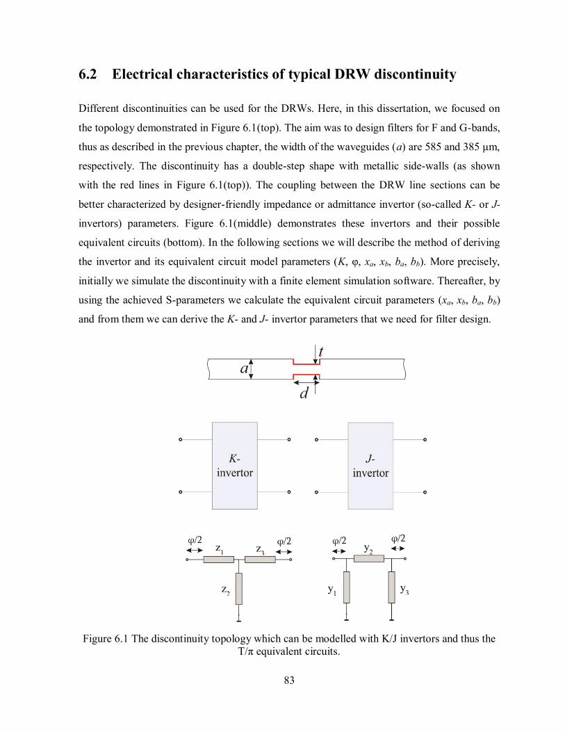
83
6.2 Electrical characteristics of typical DRW discontinuity
Different discontinuities can be used for the DRWs. Here, in this dissertation, we focused on
the topology demonstrated in Figure 6.1(top). The aim was to design filters for F and G-bands,
thus as described in the previous chapter, the width of the waveguides (a) are 585 and 385 μm,
respectively. The discontinuity has a double-step shape with metallic side-walls (as shown
with the red lines in Figure 6.1(top)). The coupling between the DRW line sections can be
better characterized by designer-friendly impedance or admittance invertor (so-called K- or J-
invertors) parameters. Figure 6.1(middle) demonstrates these invertors and their possible
equivalent circuits (bottom). In the following sections we will describe the method of deriving
the invertor and its equivalent circuit model parameters (K, φ, xa, xb, ba, bb). More precisely,
initially we simulate the discontinuity with a finite element simulation software. Thereafter, by
using the achieved S-parameters we calculate the equivalent circuit parameters (xa, xb, ba, bb)
and from them we can derive the K- and J- invertor parameters that we need for filter design.
Figure 6.1 The discontinuity topology which can be modelled with K/J invertors and thus the
T/π equivalent circuits.
y3
y2
y1
z1 z
3
z2
84
6.3 Equivalent model
Designing a filter in microwave frequencies is based on the development of equivalent model
to link the used physical structure and the electrical circuit of the filter. For the DRW,
discussed in the previous chapter, the depicted topology in Figure 6.1(top) was selected for the
waveguide discontinuity. This discontinuity should supress any propagating mode from
propagating through while the coupling should happen only through evanescent modes.
6.3.1 T-equivalent circuit
The S-parameters of the discontinuity is derived from commercially available simulation
software HFSS. Using the derived S-parameters, one can calculate the impedance matrix of
the discontinuity using equation
[ ] [ ] [ ] [ ] [ ] 6.1
where [S] is the 2 × 2 scattering matrix and [I] is the unity matrix with the same dimension.
With this matrix one can calculate the reactances (xa and xb) in T-equivalent circuit of Figure
6.1(bottom). In the same manner, one can derive the susceptance (bb and ba) of the π-
equivalent circuit using the [Y] matrix. Since the silicon used for the DRW is isotropic, linear,
and homogeneous, the discontinuity’s topology studied are reciprocal and the resulting
impedance matrix is symmetric, which is written
6.2 6
This will result in the following relations between the impedances of T-circuit and elements of
impedance matrix.
6.3

85
Moreover, since the discontinuity structure is symmetrical the following relationship can be
written
6.4
Finally, since the dielectric losses are neglected and the radiated power from DRW is very
small we have
( ) 6.5
for all and means the real part of the complex value x. Although the
losses in equation 6.5 are neglected, this method will give the initial values and further
optimizations are necessary to achieve the desired performance. The equations 6.3-6.5 allows
for finding the normalized reactances of equivalent model xa, xb and xc defined as
,
6.6
6.3.2 Impedance invertor
It is also very useful to introduce an equivalent model involving an impedance inverter as
shown in Figure 6.1(middle). This notion of inverter has been widely studied and commonly
used in the field of microwave [138]. Formulas 6.7 (indicated below) show a way of going
from standard T-model to model with normalized impedance inverter. The same formula may
be used to derive the admittance invertor just by replacing xa, xb and Z0 with ba, bb and Y0,
respectively.
6.7
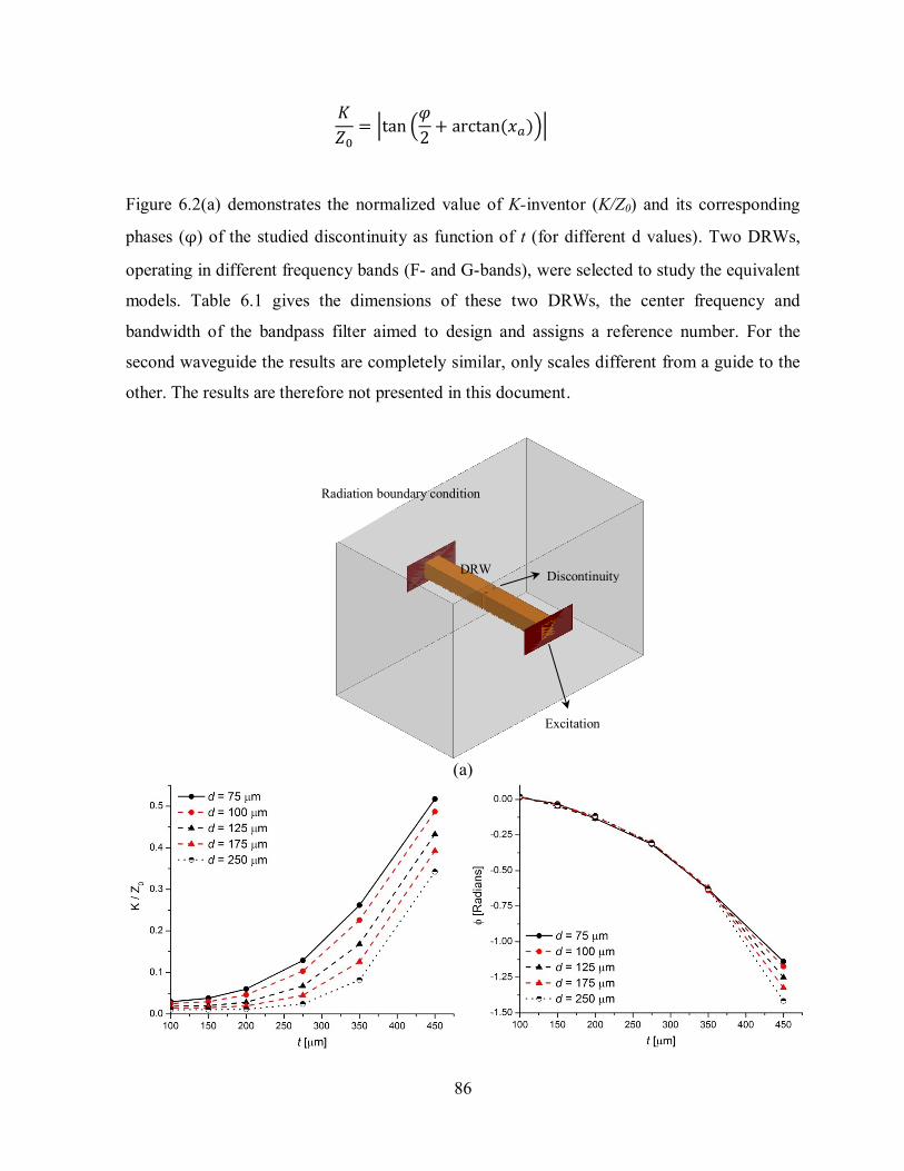
86
| (
)|
Figure 6.2(a) demonstrates the normalized value of K-inventor (K/Z0) and its corresponding
phases (φ) of the studied discontinuity as function of t (for different d values). Two DRWs,
operating in different frequency bands (F- and G-bands), were selected to study the equivalent
models. Table 6.1 gives the dimensions of these two DRWs, the center frequency and
bandwidth of the bandpass filter aimed to design and assigns a reference number. For the
second waveguide the results are completely similar, only scales different from a guide to the
other. The results are therefore not presented in this document.
(a)
Excitation
Discontinuity DRW
Radiation boundary condition
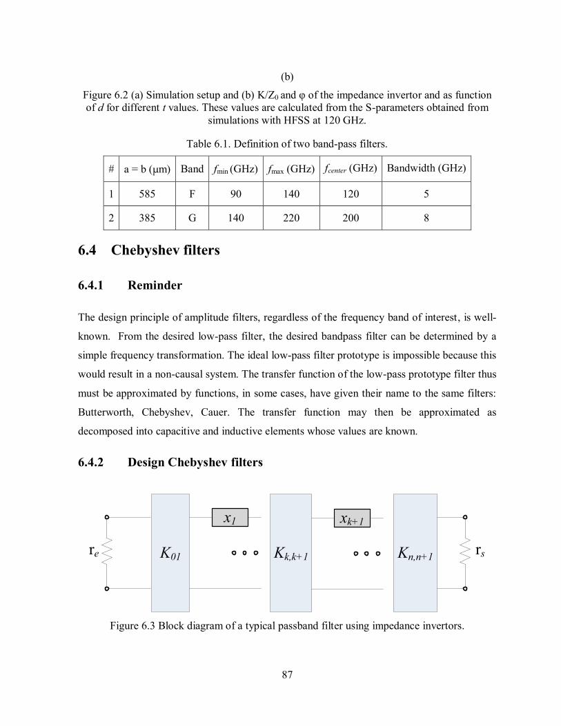
87
(b)
Figure 6.2 (a) Simulation setup and (b) K/Z0 and φ of the impedance invertor and as function
of d for different t values. These values are calculated from the S-parameters obtained from
simulations with HFSS at 120 GHz.
Table 6.1. Definition of two band-pass filters.
# a = b (μm) Band fmin (GHz) fmax (GHz) fcenter (GHz) Bandwidth (GHz)
1 585 F 90 140 120 5
2 385 G 140 220 200 8
6.4 Chebyshev filters
6.4.1 Reminder
The design principle of amplitude filters, regardless of the frequency band of interest, is well-
known. From the desired low-pass filter, the desired bandpass filter can be determined by a
simple frequency transformation. The ideal low-pass filter prototype is impossible because this
would result in a non-causal system. The transfer function of the low-pass prototype filter thus
must be approximated by functions, in some cases, have given their name to the same filters:
Butterworth, Chebyshev, Cauer. The transfer function may then be approximated as
decomposed into capacitive and inductive elements whose values are known.
6.4.2 Design Chebyshev filters
K01
x1
Kk,k+1re
xk+1
Kn,n+1rs
Figure 6.3 Block diagram of a typical passband filter using impedance invertors.

88
Low-pass filter prototype can be transformed into its composing impedance inverters [138],
[139]. This transformation leads to the block of the Figure 6.3 representing a general pattern of
bandpass filters. This diagram represents a series of resonators defined by their normalized
reactance xk, coupling them through impedance inverters. The theoretical values of the
impedance inverter are given by the following equations:
√
√
√
6.8
with ⁄ and √ . The [ ] are the values of the discrete
components of bandpass prototype and are given in [138]. The [ ] are the slope
parameters and are defined in the following subsection. Finally, the re and rs values are,
respectively, the normalized impedances of input and output. Since the inlet and outlet of the
guide are formed of a same resonator guide, these standard impedances are equal to one.
Slope parameters of a resonator
By definition [138], the slope parameter of a resonator is given by the following formula
|
6.9
where X(ω) is the reactance of resonators.
If the resonator is a transmission line of length l, short-circuited at the end, the reactance is
89
6.10
this transmission line resonates at the frequency where which leads to the definition
of the length of the resonator
for all and where is the guided wavelength of the transmission line at .
Using equations 6.9 and 6.10, the slope parameter of the short-circuited transmission line can
be calculated as
|
→
|
6.11
For the case of a short-circuited DRW half-wavelength resonator we can rewrite the x as
|
|
6.12
Therefore, equations 6.8 can be rewritten
90
√
√
√
6.13
K values derived from equation 6.13 should be used to select the proper t, d in Figure 6.2(a).
Also, from Figure 6.2(a) one can obtain the φ values and use following equation to derive the
jth resonator lengths.
[ ]
6.14
Optimization
Commercially available software package (HFSS), is used to optimize the initial values
derived from the above formulation. A parametric study is performed to obtain a bandpass
filter at center frequency of 120 GHz and bandwidth of 5 GHz. The S-parameters and
dimensions of the designed third and fifth order filters are reported in Figure 6.4. These
preliminary results show the feasibility of realizing bandpass filters with DRWs. Fabrication
and experimental verification of the designed filters are in process.

91
(a)
(b)
Figure 6.4 (a) 5th order bandpass filter and (b) Simulation results derived from HFSS. The
dimensions for the 3rd
order filter are t1 = 145, t2 = 90 μm, l1 = 488 μm, l2 = 448 μm and d1 =
d2 = 75μm. Also, for the 5th order filter the dimensions are t1 = 275 μm, t2 = 290 μm, t3 = 380
μm, l1 = 454 μm, l2 = 447 μm, l3 = 403 μm and d1 = d2 = d3 = 75 μm.
6.5 Conclusion
A third and fifth order bandpass filters are designed for the center frequency of 120 GHz.
Using a conventional filter design technique, an introduced discontinuity is studied and
modeled and then used in an equivalent model and circuit for filter design . The values of
lumped elements are achieved for the desired center frequency and bandwidth and then
replaced with proper discontinuity. The simulations demonstrate the potentiality of the
proposed DRWs proposed in chapter 5 as the host waveguide for the filter design.
l1 l
2 l
2 l
3
l3
d1 d
1 d
2 d
2 d
3 d
3
t1 t
1 t
2 t
3 t
3 t
2
92
7 CONCLUSION AND FUTURE WORK
The principal objective of this work was to investigate novel materials and solutions for
guiding THz waves. Two materials, graphene and HR-silicon, were used to develop new
waveguides. Through the study of PPWG with graphene layers, a dispersion equation is
derived allowing calculation of propagation constant for different waveguides including
dielectric slabs with conductor plates on top and bottom with possibility of selection of
arbitrary and different conductivity (both σd and σh) values for the plates. Chapter 4, 5 and 6
are dedicated to study of the HR-silicon waveguide solutions. A HR-silicon slab waveguide is
characterized with THz-TDS system to prove the low-loss and low-dispersive properties of
HR-silicon. Then, this material is used to develop a DRW to eliminate the wave broadening
losses in the slab waveguide. The provided proof of concept for DRWs opens a window
toward future dominant technology in THz wave guiding. Researches on scrutinizing the HR-
silicon based DRW properties and capabilities, some listed below, are foreseen.
7.1 Conclusions
Here are the important results of this research:
The study of parallel plate waveguide with graphene layers demonstrated that although
the guide shows interesting capabilities but the losses are still high at THz frequencies
in comparison with current state of the art. Nevertheless, due to the unique properties
of the proposed waveguide, it can be considered for specific applications.
It is difficult to perform experiments with graphene layers as they are very sensitive to
the applied voltage. By increasing the gate voltage and by exceeding over a certain
limit, which is different form sample to sample, the graphene layer will leak or even
be destroyed. This obstacle has limited our researches on graphene to only theoretical
investigations. With advent of novel graphene growth techniques on different
substrates hope that these problems will solve in future.

93
Based on the characterization of HR-silicon dielectric slab waveguide, the low-loss
and low-dispersive nature of this material and the waveguide are proved. Therefore,
HR-silicon can extensively be used for THz waves handling. It is shown that, as the
wave enters the HR-silicon slab it starts broadening and thus introduces losses.
The simulations and measurements performed to study the dielectric ribbon waveguide
demonstrated a very good performance in terms of loss and dispersion. Including the
low-cost fabrication process, DRWs can be very good candidate for THz wave
propagation. A measurement setup is then suggested that can connect the dielectric
waveguides to standard flanges. The proposed connection mechanism shows a low
sensitivity to alignments.
The conventional methods can be employed to design bandpass filters for THz band
using DRWs. The filters are designed by studying an arbitrary discontinuity using
HFSS simulator. Based on the designed method, different other discontinuities and
topologies can be used for synthesis of bandpass filters.
7.2 Suggested future work
1. Chapter 3 investigates theoretically the properties of the graphene PPWG. Currently,
by advent of new graphene growth techniques one can study the properties of this
waveguide experimentally. This can be accomplished by using two conductor backed
graphene substrates and shall be mounted a high magnetic field source.
2. As discussed earlier, DRWs have the potential to become the dominant technology in
THz wave guiding. Therefore, other passive components such as bends, couplers,
antennas and power dividers should be studied both theoretically and experimentally.
3. Based on the low-cost and straight forward fabrication process, development of DRWs
for higher frequencies are feasible. Also, the design method provided should be
employed to design DRWs with different host materials to clarify the advantages of
HR-silicon.

94
4. Transitions are essential element for connecting different circuits and components.
Therefore, study of transitions form DRW to rectangular and circular waveguide,
CPWs, microstrip lines, strip lines and slot lines should be investigated. The sensitivity
and misalignment effects of DRW in the above transition are important in high
frequency applications and thus have to be determined.
7.3 Conclusions (en français)
Les résultats importants de cette thèse peuvent être résumés comme suit:
L'étude du guide d'onde à plaques parallèle utilisant du graphène montre d'intéressantes
propriétés mais les pertes évaluées sont trop grande pour les fréquences térahertz.
Néanmoins, du fait des propriétés clairement analysées, ce type de guide peut être
utilisé dans des applications spécifiques.
Il est très difficile de mener des expériences avec des couches de graphène puisque ce
dernier est très sensible à l'excitation électrique. En augmentant la «tension de grille»,
on peut dépasser un seuil critique, variable d'un échantillon à l'autre, conduisant à
l'apparition d'un courant de fuite potentiellement destructif. Ceci est un facteur limitant
pour la recherche actuelle mais les développements sur la croissance du graphène sur
différents substrats laissent espérer une résolution du problème.
En se basant sur la caractérisation d'une couche de silicium à haute résistivité, la nature
faible perte et faible dispersion de ce matériau a été démontré, ouvrant la voie à son
utilisation pour supporter et guider des ondes térahertz.
Des mesures à l'aide d'un système de spectroscopie temporel ont confirmé les faibles
pertes et la faible dispersion de ce matériau. Cependant, si l'on utilise une couche de
diélectrique, l'onde se propage non seulement le long de la direction voulue mais
également de façon transverse, ce qui introduit des pertes supplémentaires.
95
L'utilisation d'une tige de diélectrique semble empêcher ce phénomène, ce qui a été
démontré à la fois théoriquement et par des mesures et le guide d'onde résultant
présente de très bonnes performances en terme de dispersion et de pertes. Un tel guide
peut s'avérer un très bon choix dans la plage des fréquences THz. Un banc de mesure a
été proposé pour s'adapter aux guides d'ondes rectangulaires classiques. On note une
grande tolérance au désalignement des deux parties.
Les méthodes conventionnelles peuvent être utilisées pour concevoir des filtres dans la
bande de fréquence térahertz en utilisant ce type de guide. Un filtre passe-bande a été
conçu en analysant un type de discontinuité à l'aide du logiciel HFSS et d'autres
discontinuités peuvent servir d'éléments de base dans la conception de tels filtres.
7.4 Travaux futurs
1. Dans le chapitre 3, le guide à plaques parallèles utilisant du graphène a été étudié
théoriquement. De façon pratique, on pourrait déposer deux couches de graphène sur
un substrat entre lesquelles une tension serait appliquée et le tout serait plongé dans un
champ magnétique.
2. Comme démontré par cette thèse, un guide formé d'une tige de HR-Si a le potentiel de
devenir un guide de référence dans la bande de fréquence térahertz. Aussi, d'autres
composants comme des coupleurs, des antennes ou des diviseurs de puissances
pourraient être étudiés théoriquement et expérimentalement pour démontrer et
développer les possibilités de cette technologie.
3. Les guides à base de HR-Si tels qu'étudiés dans cette thèse sont réalisés à l'aide d'un
procédé simple de fabrication. Aussi cette méthode de fabrication pourrait être utilisée
sur d'autres matériaux que le HR-Si pour clarifier et mettre en évidence l'avantage de
ce matériau.
4. Les transitions sont des éléments essentiels pour connecter les composants entre eux et
même des circuits. Aussi, l'étude de transitions entre le guide HR-Si et les guides

96
courants tels que les guides rectangulaires et circulaire, les guides planaires
(microstrip, slot-line, coplanaire, triplaque) devraient être étudiées. La sensibilité du
désalignement des guides dans ce genre de transition peut être importante et mérite
d'être étudiée et caractérisée.
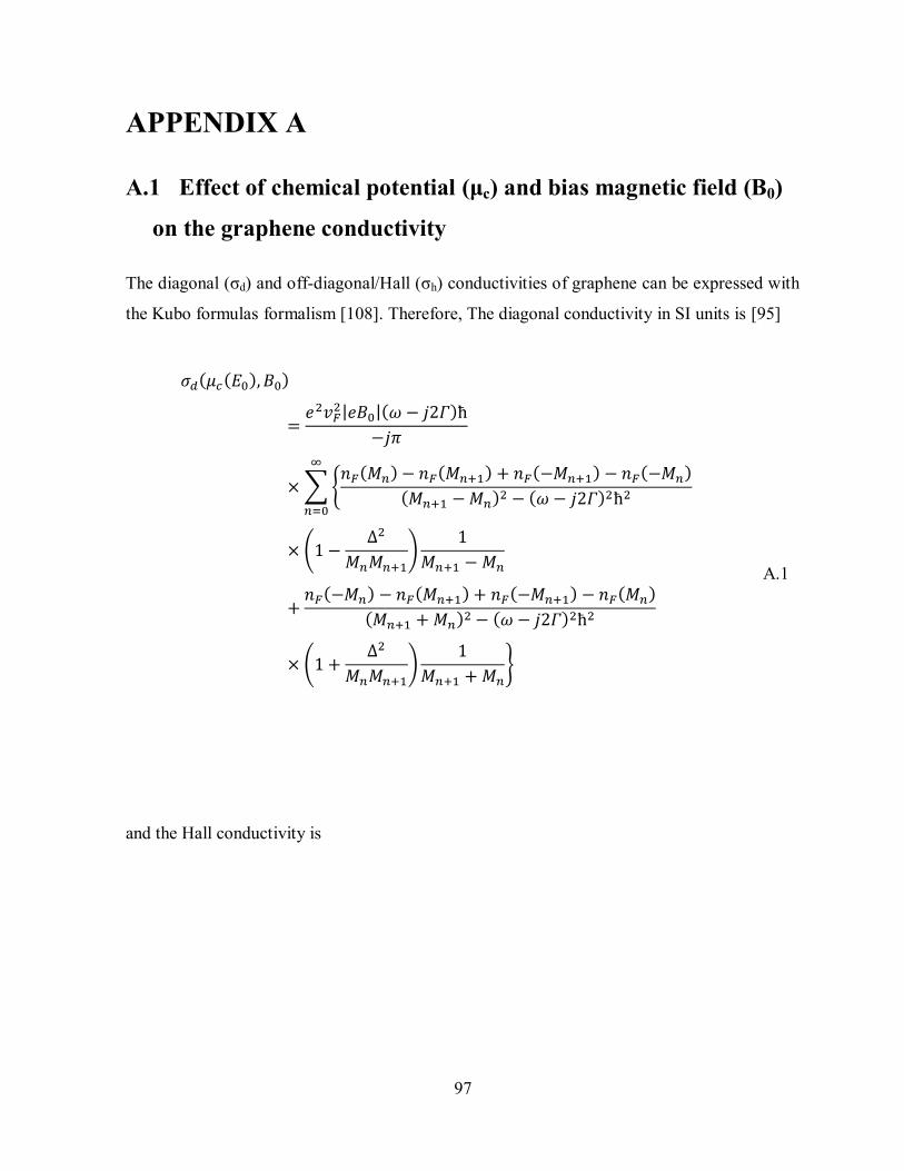
97
APPENDIX A
A.1 Effect of chemical potential (μc) and bias magnetic field (B0)
on the graphene conductivity
The diagonal (σd) and off-diagonal/Hall (σh) conductivities of graphene can be expressed with
the Kubo formulas formalism [108]. Therefore, The diagonal conductivity in SI units is [95]
| |
∑
(
)
(
)
A.1
and the Hall conductivity is
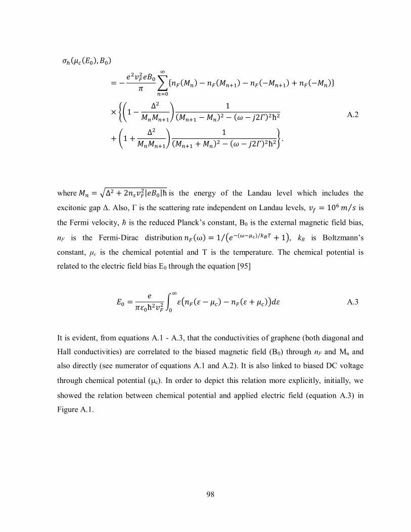
98
∑
(
)
(
)
A.2
where √ | | is the energy of the Landau level which includes the
excitonic gap Δ. Also, Γ is the scattering rate independent on Landau levels, ⁄ is
the Fermi velocity, ħ is the reduced Planck’s constant, B0 is the external magnetic field bias,
nF is the Fermi-Dirac distribution ( )⁄ , kB is Boltzmann’s
constant, μc is the chemical potential and T is the temperature. The chemical potential is
related to the electric field bias E0 through the equation [95]
∫ ( )
A.3
It is evident, from equations A.1 - A.3, that the conductivities of graphene (both diagonal and
Hall conductivities) are correlated to the biased magnetic field (B0) through nF and Mn and
also directly (see numerator of equations A.1 and A.2). It is also linked to biased DC voltage
through chemical potential (μc). In order to depict this relation more explicitly, initially, we
showed the relation between chemical potential and applied electric field (equation A.3) in
Figure A.1.
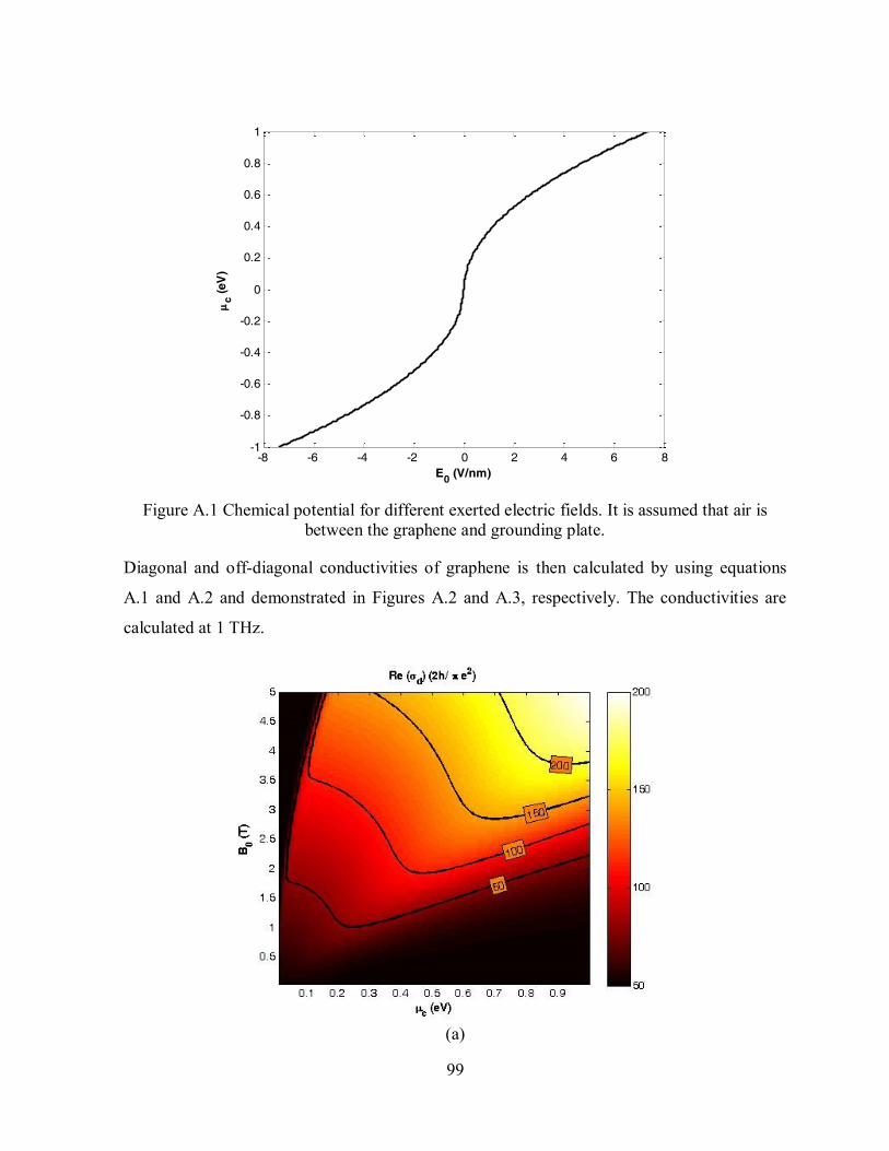
99
Figure A.1 Chemical potential for different exerted electric fields. It is assumed that air is
between the graphene and grounding plate.
Diagonal and off-diagonal conductivities of graphene is then calculated by using equations
A.1 and A.2 and demonstrated in Figures A.2 and A.3, respectively. The conductivities are
calculated at 1 THz.
(a)
-8 -6 -4 -2 0 2 4 6 8-1
-0.8
-0.6
-0.4
-0.2
0
0.2
0.4
0.6
0.8
1
c (
eV
)
E0 (V/nm)

100
Figure A.2 (a) Normalized intensity of real and (b) imaginary parts of diagonal conductivity of
graphene at 1 THz calculated from equation A.1. It is assumed that ⁄ ,
and T=300 ˚K.
(a)
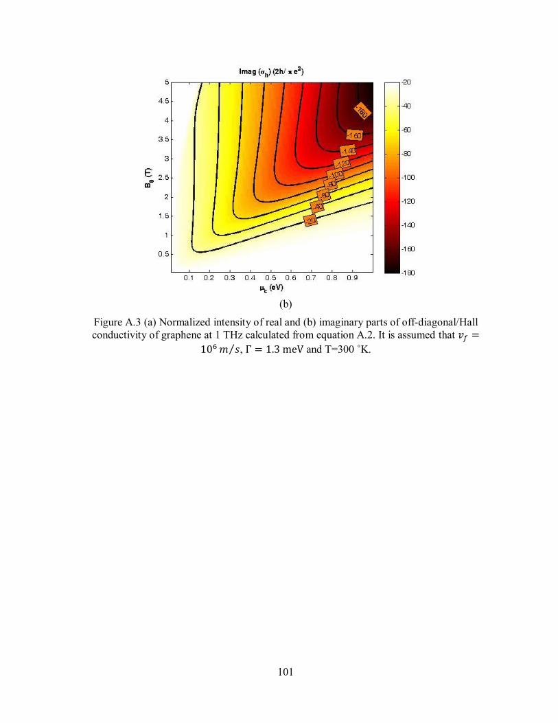
101
(b)
Figure A.3 (a) Normalized intensity of real and (b) imaginary parts of off-diagonal/Hall
conductivity of graphene at 1 THz calculated from equation A.2. It is assumed that
⁄ , and T=300 ˚K.

102
APPENDIX B
B.1 Deriving the dispersion equation 3.8
Here, in this appendix, a complete and detailed derivation of the dispersion equations in
chapter 3 (equations 3.8 and 3.15) are presented. We will start from Maxwell’s equations and
will derive the dispersion equations of PEC-graphene and graphene-graphene waveguides.
Starting from Maxwell’s equations and assuming a source free environment we have
B.1
with an z-dependence. Each of the above Maxwell’s equations can be expanded to three
other sub-equations (for x, y, z-directions) as:
B.2
One can write the four components of the electric and magnetic fields in terms of the two
other components. For example Ex, Ey, Hx, Hy can be expressed in terms of electromagnetic
fields Ez, Hz

103
(
)
(
)
(
)
(
)
B.3
where
is the cutoff wavenumber, km is the wavenumber and for the
medium I and II (considering the PEC-graphene waveguide case shown in Figure 3.1). In
order to obtain the z-components of electric (Ez) and magnetic (Hz) fields, one may solve the
wave equations in region I and II, resulting in
B.4
where and
. In the above equations A1, A2, B1, B2 and
β are unknowns. Therefore, the other components electromagnetic fields in region II can be
achieved from equation B.3
B.5
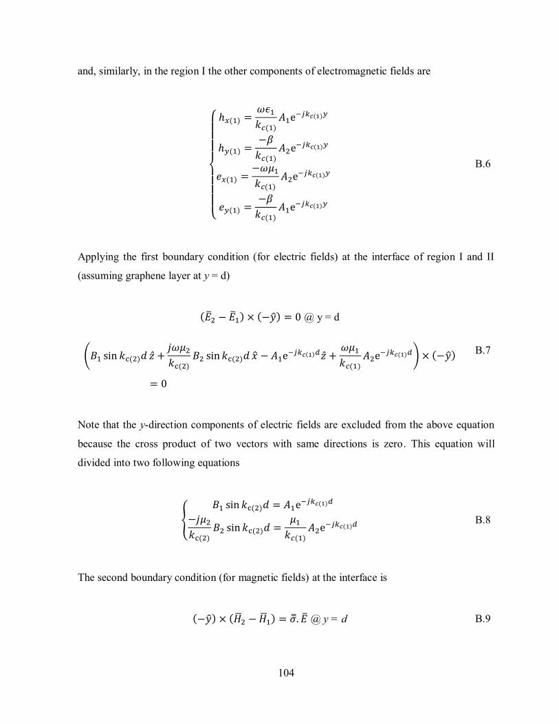
104
and, similarly, in the region I the other components of electromagnetic fields are
B.6
Applying the first boundary condition (for electric fields) at the interface of region I and II
(assuming graphene layer at y = d)
@ y = d
(
)
B.7
Note that the y-direction components of electric fields are excluded from the above equation
because the cross product of two vectors with same directions is zero. This equation will
divided into two following equations
B.8
The second boundary condition (for magnetic fields) at the interface is
@ y = d B.9

105
(
)
where
(
) (
) B.10
Sign of the hall conductivity is related to the direction of the magnetic field (B0 in Figure 3.1)
which dictates the carrier motion. Figure B.1 depicts a procedure to select the proper sign for
Hall conductivity. Considering the +x-direction electric field (Ex in Figure B.1 top), the
electron feels an electric force (Fe = -e Ex) toward the –x-direction. Also, a Lorentz force (Fm)
will be toward the +z-direction. Therefore, the current, which is the motion of the positive
charge (opposite of electron direction), created by the Ex may be written
B.11
Hence, here for the setup shown in Figure 3.1, we used a positive sign for the Hall
conductivity in the first row of the matrix and thus a minus sign for the second row (which is
also observable from Figure A.1 bottom). Therefore, we have
(
) (
) ( ) ( ) B.12
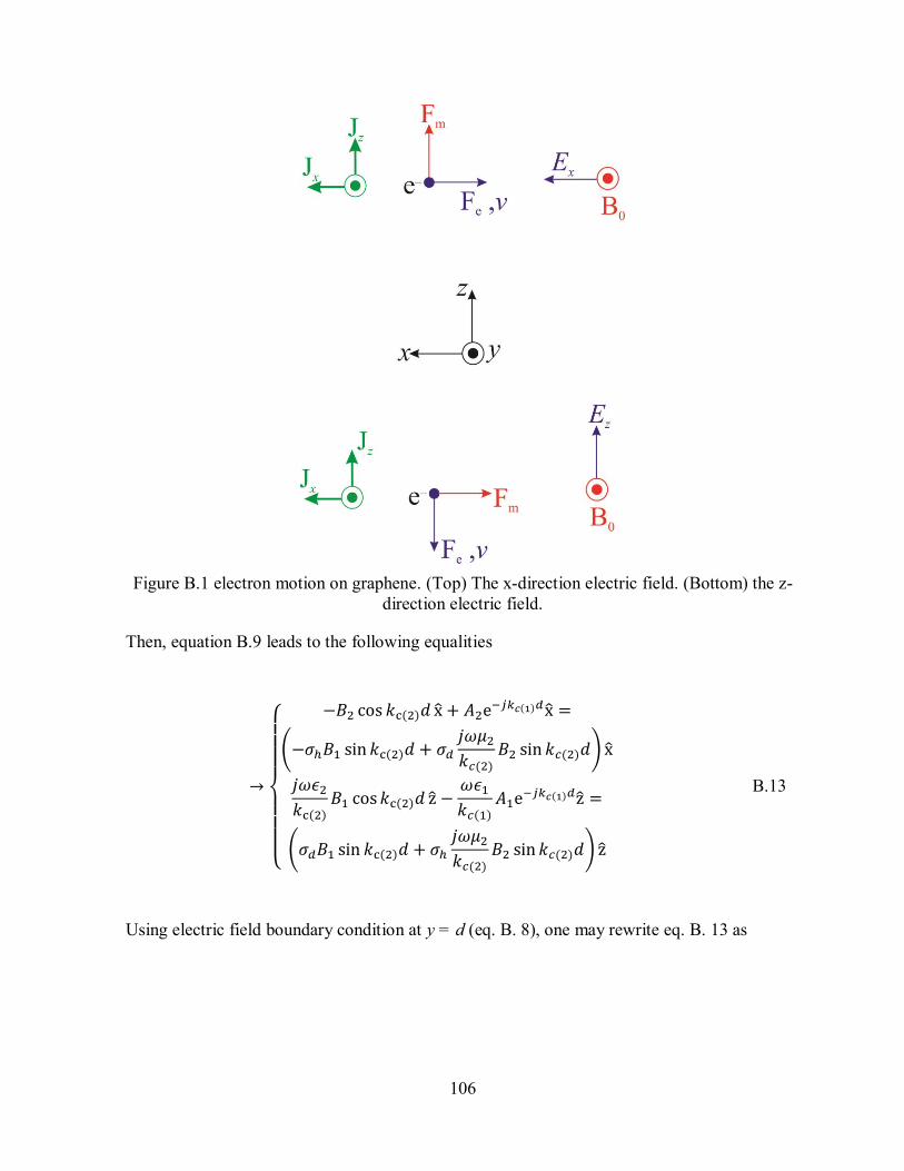
106
Figure B.1 electron motion on graphene. (Top) The x-direction electric field. (Bottom) the z-
direction electric field.
Then, equation B.9 leads to the following equalities
(
)
(
)
B.13
Using electric field boundary condition at y = d (eq. B. 8), one may rewrite eq. B. 13 as

107
B.14
So in the above series of equations, B1 and B2 are unknowns. Therefore, in order to have
nontrivial solution the determinant of the two above equations must vanish, leading to the
dispersion equation which is
[ (
)] [ (
)]
B.15
B.2 Deriving the dispersion equation 3.15
Similar to the PEC-graphene plate case, here, the derivation process of dispersion equation
3.15 will be described. The process includes solving the wave equation in the mediums I, II
and III (see Figure 3.5) and applying the boundary conditions at y = 0 and y = d. As we also
discussed in the previous section, the electric and magnetic fields can be written for medium II
as (note that the tangential electric field shouldn’t vanish at y = 0 because, unlike the PEC-
graphene case, there is no PEC at y = 0.)
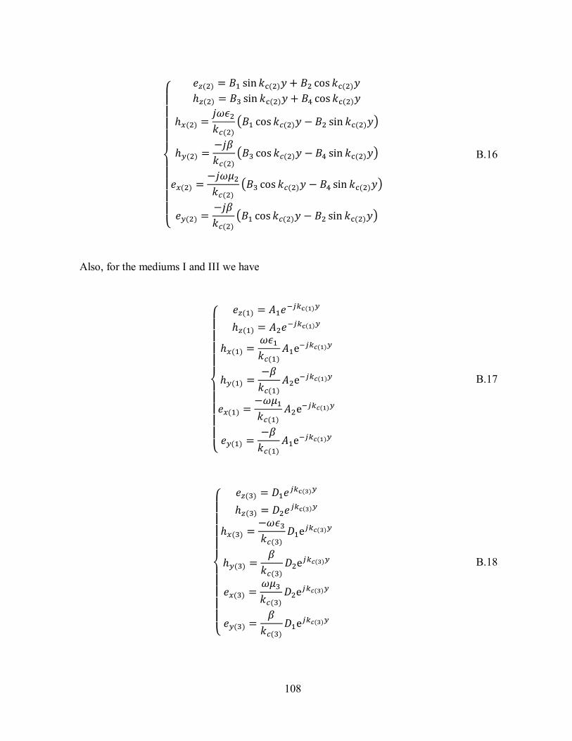
108
( )
( )
( )
( )
B.16
Also, for the mediums I and III we have
B.17
B.18
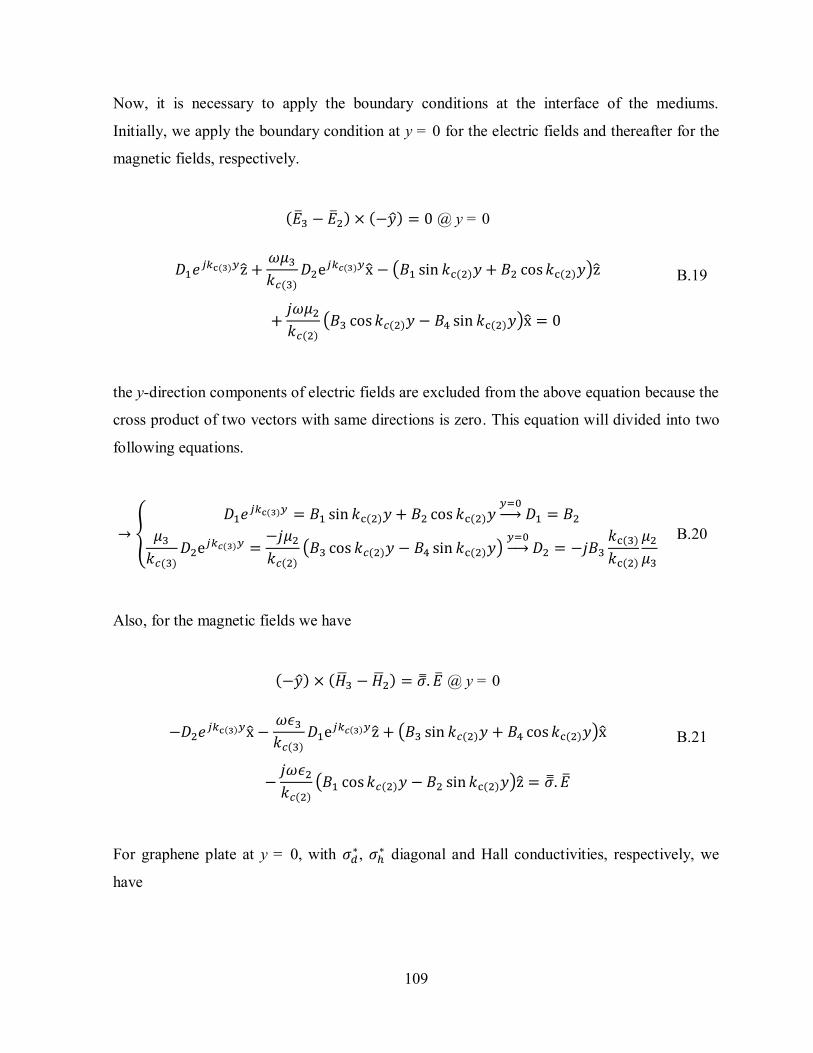
109
Now, it is necessary to apply the boundary conditions at the interface of the mediums.
Initially, we apply the boundary condition at y = 0 for the electric fields and thereafter for the
magnetic fields, respectively.
@ y = 0
( )
( )
B.19
the y-direction components of electric fields are excluded from the above equation because the
cross product of two vectors with same directions is zero. This equation will divided into two
following equations.
→
( )
→
B.20
Also, for the magnetic fields we have
@ y = 0
( )
( )
B.21
For graphene plate at y = 0, with ,
diagonal and Hall conductivities, respectively, we
have
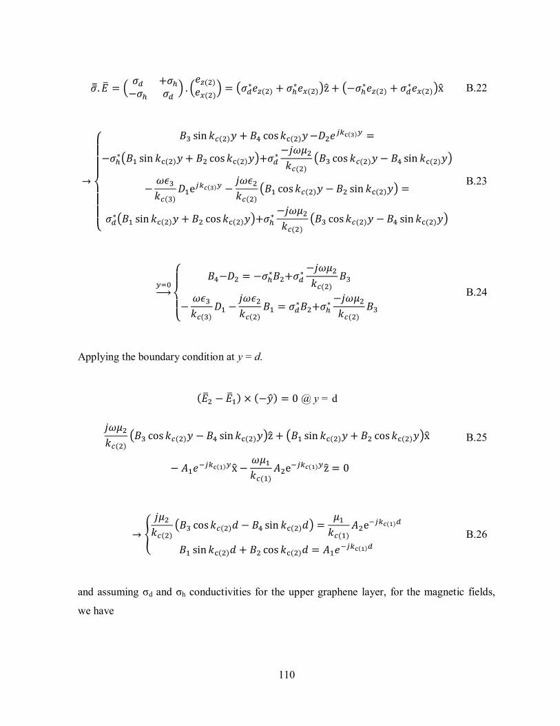
110
(
) (
) (
) (
) B.22
( )
( )
( )
( )
( )
B.23
→
B.24
Applying the boundary condition at y = d.
@ y = d
( ) ( )
B.25
( )
B.26
and assuming σd and σh conductivities for the upper graphene layer, for the magnetic fields,
we have

111
@ y = d
( )
( )
( ) ( )
B.27
( )
( )
B.28
From electric fields boundary condition at y = d (equations B.26), A1 and A2 can replace in
terms of B3 and B4 in the above equation and thus one can write
( )
( )
( )
( )
( )
( )
( )
( )
B.29
Here, we have two equations and there are four unknowns. Therefore, we need to bring two
other equations to solve the system equation. To do so, we use the electric and magnetic fields
boundary conditions at y = 0 (equations B.20 and B.24). In equation B.20, one can replace D1
and D2 with expressions in terms of B1, B2, B3 and B4 using equation B.24 the
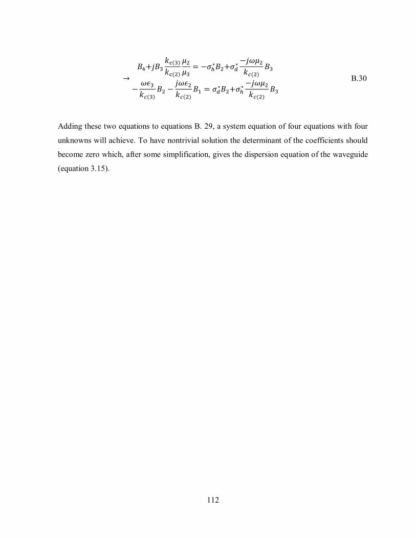
112
B.30
Adding these two equations to equations B. 29, a system equation of four equations with four
unknowns will achieve. To have nontrivial solution the determinant of the coefficients should
become zero which, after some simplification, gives the dispersion equation of the waveguide
(equation 3.15).
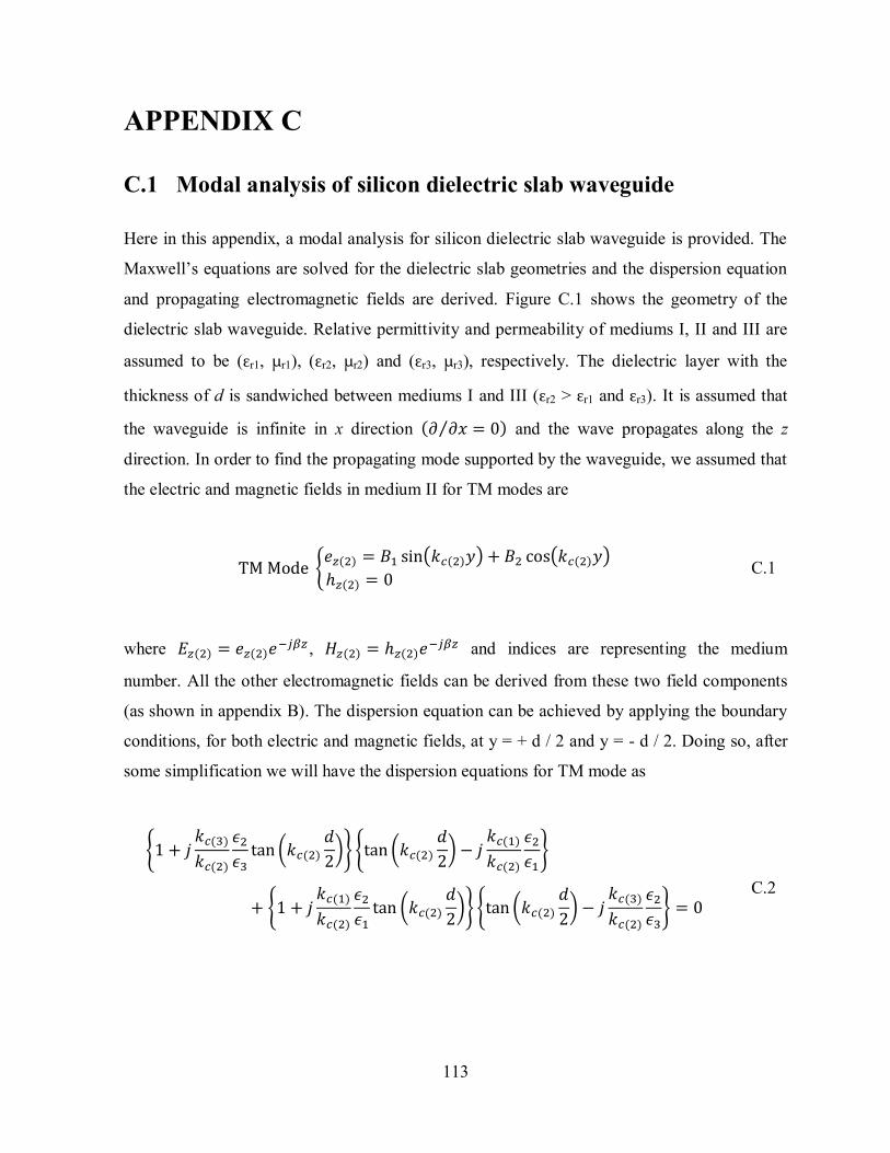
113
APPENDIX C
C.1 Modal analysis of silicon dielectric slab waveguide
Here in this appendix, a modal analysis for silicon dielectric slab waveguide is provided. The
Maxwell’s equations are solved for the dielectric slab geometries and the dispersion equation
and propagating electromagnetic fields are derived. Figure C.1 shows the geometry of the
dielectric slab waveguide. Relative permittivity and permeability of mediums I, II and III are
assumed to be (εr1, μr1), (εr2, μr2) and (εr3, μr3), respectively. The dielectric layer with the
thickness of d is sandwiched between mediums I and III (εr2 > εr1 and εr3). It is assumed that
the waveguide is infinite in x direction ⁄ and the wave propagates along the z
direction. In order to find the propagating mode supported by the waveguide, we assumed that
the electric and magnetic fields in medium II for TM modes are
( ) ( )
C.1
where ,
and indices are representing the medium
number. All the other electromagnetic fields can be derived from these two field components
(as shown in appendix B). The dispersion equation can be achieved by applying the boundary
conditions, for both electric and magnetic fields, at y = + d / 2 and y = - d / 2. Doing so, after
some simplification we will have the dispersion equations for TM mode as
(
) (
)
(
) (
)
C.2
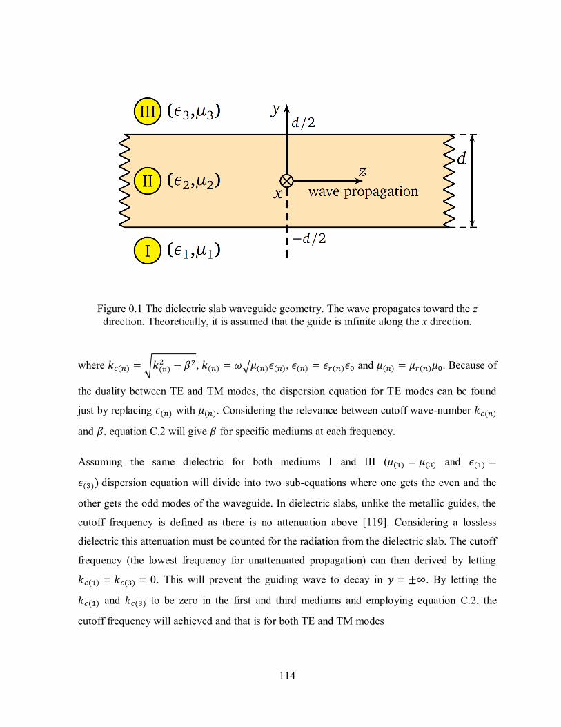
114
Figure 0.1 The dielectric slab waveguide geometry. The wave propagates toward the z
direction. Theoretically, it is assumed that the guide is infinite along the x direction.
where √ , √ , and . Because of
the duality between TE and TM modes, the dispersion equation for TE modes can be found
just by replacing with . Considering the relevance between cutoff wave-number
and , equation C.2 will give for specific mediums at each frequency.
Assuming the same dielectric for both mediums I and III ( and
dispersion equation will divide into two sub-equations where one gets the even and the
other gets the odd modes of the waveguide. In dielectric slabs, unlike the metallic guides, the
cutoff frequency is defined as there is no attenuation above [119]. Considering a lossless
dielectric this attenuation must be counted for the radiation from the dielectric slab. The cutoff
frequency (the lowest frequency for unattenuated propagation) can then derived by letting
. This will prevent the guiding wave to decay in . By letting the
and to be zero in the first and third mediums and employing equation C.2, the
cutoff frequency will achieved and that is for both TE and TM modes

115
√ C.3
Figure C.2 depicts the normalized propagation constant of 100 μm thick silicon slab
waveguide. One can see that both TMn and TEn modes have the same cutoff frequency. Also,
the cutoff frequency of the first modes (TM0 and TE0) is zero. It is obvious that the for 100 μm
thick silicon slab a multi-mode propagation happens for the THz pulsed signal. By increasing
the thickness of the slab the number of the modes in the specific band will increase as the
cutoff frequency of the modes decrease (see the above equation for the cutoff frequency).
(a)
0 200 400 600 800 10001
1.5
2
2.5
3
Frequency [GHz]
/ k
0
TE0
TM0
TE1
TM1
TE2
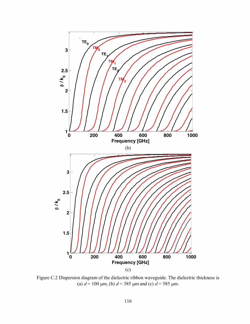
116
(b)
(c)
Figure C.2 Dispersion diagram of the dielectric ribbon waveguide. The dielectric thickness is
(a) d = 100 μm, (b) d = 385 μm and (c) d = 585 μm.
0 200 400 600 800 10001
1.5
2
2.5
3
Frequency [GHz]
/ k
0
TE0
TM1
TE1
TM0
TE2
TM2
0 200 400 600 800 10001
1.5
2
2.5
3
Frequency [GHz]
/ k
0

117
REFERENCES
[1] X.-C. Zhang and J. Xu, Introduction to THz Wave Propagation. Heidelberg: Springer,
2010.
[2] A. Rostami, H. Rasooli, and H. Baghban, THz technology Fundamentals and
applications. Heidelberg: Springer, 2011.
[3] Y.-S. Lee, Principles of Terahertz Science and Technology, vol. 108. 2008, p. 347.
[4] P. H. Siegel, “Terahertz technology,” IEEE Trans. Microw. Theory Tech., vol. 50,
2002.
[5] H. Song, T. Nagatsuma, S. Member, and I. Paper, “Present and Future of Terahertz
Communications,” vol. 1, no. 1, pp. 256–263, 2011.
[6] Y. Yang, M. Mandehgar, and D. R. Grischkowsky, “Broadband THz Pulse
Transmission Through the Atmosphere,” IEEE Trans. Terahertz Sci. Technol., vol. 1,
pp. 264–273, 2011.
[7] Y. Yang, M. Mandehgar, and D. R. Grischkowsky, “Understanding THz Pulse
Propagation in the Atmosphere,” IEEE Transactions on Terahertz Science and
Technology, vol. 2. pp. 406–415, 2012.
[8] C. Fattinger and D. Grischkowsky, “Point source terahertz optics,” Appl. Phys. Lett.,
vol. 53, p. 1480, 1988.
[9] C. Fattinger and D. Grischkowsky, “Terahertz beams,” Appl. Phys. Lett., vol. 54, p.
490, 1989.
[10] M. Vanexter, C. Fattinger, and D. Grischkowsky, “High-brightness terahertz beams
characterized with an ultrafast detector,” Appl. Phys. Lett., vol. 55, p. 337, 1989.
[11] G. Zhao, R. N. Schouten, N. van der Valk, W. T. Wenckebach, and P. C. M. Planken,
“Design and performance of a THz emission and detection setup based on a semi-
insulating GaAs emitter,” Rev. Sci. Instrum., vol. 73, p. 1715, 2002.
[12] F. Ward, G. Weinreich, M. Bass, and P. A. Franken, “Optical Rectification,” phsical
Rev. Lett., vol. 9, no. 11, pp. 28–31, 1962.
[13] M. Suzuki and M. Tonouchi, “Fe-implanted InGaAs terahertz emitters for 1.56 μm
wavelength excitation,” Appl. Phys. Lett., vol. 86, p. 051104, 2005.
[14] P. Y. Han and X. C. Zhang, “Coherent, broadband midinfrared terahertz beam sensors,”
Appl. Phys. Lett., vol. 73, p. 3049, 1998.
118
[15] R. Huber, a Brodschelm, F. Tauser, and a Leitenstorfer, “Generation and field-resolved
detection of femtosecond electromagnetic pulses tunable up to 41 THz,” Appl. Phys.
Lett., vol. 76, p. 3191, 2000.
[16] W. Knap, Y. Deng, S. Rumyantsev, and M. S. Shur, “Resonant detection of
subterahertz and terahertz radiation by plasma waves in submicron field-effect
transistors,” Appl. Phys. Lett., vol. 81, p. 4637, 2002.
[17] M. Liang and X. Hao, “Microwave to Terahertz,” Microw. Mag., no. February, pp. 40–
51, 2014.
[18] A. Mehdipour, I. D. Rosca, A.-R. Sebak, C. W. Trueman, and S. V. Hoa, “Carbon
Nanotube Composites for Wideband Millimeter-Wave Antenna Applications,” IEEE
Trans. Antennas Propag., vol. 59, pp. 3572–3578, 2011.
[19] J. Clifford, D. L. John, and D. L. Pulfrey, “Bipolar conduction and drain-induced
barrier thinning in carbon nanotube FETs,” IEEE Trans. Nanotechnol., vol. 2, 2003.
[20] O. Mitrofanov, R. James, F. A. Fernandez, T. K. Mavrogordatos, and J. A. Harrington,
“Reducing Transmission Losses in Hollow THz Waveguides,” IEEE Trans. Terahertz
Sci. Technol., vol. 1, pp. 124–132, 2011.
[21] A. Dupuis, “Dielectric THz Waveguides,” Ph.D. dissertation, École Polytechnic de
Montreal, 2010.
[22] M. Y. Frankel, S. Gupta, J. A. Valdmanis, and G. A. Mourou, “Terahertz attenuation
and dispersion characteristics of coplanar transmission lines,” IEEE Trans. Microw.
Theory Tech., vol. 39, 1991.
[23] R. W. McGowan, G. Gallot, and D. Grischkowsky, “Propagation of ultrawideband short
pulses of terahertz radiation through submillimeter-diameter circular waveguides.,”
Opt. Lett., vol. 24, pp. 1431–1433, 1999.
[24] G. Gallot, S. P. Jamison, R. W. McGowan, and D. R. Grischkowsky, “Terahertz
Waveguides,” J. Otical Soc. Amterica B, vol. 17, no. 5, pp. 851–863, 2000.
[25] J. Harrington, R. George, P. Pedersen, and E. Mueller, “Hollow polycarbonate
waveguides with inner Cu coatings for delivery of terahertz radiation.,” Opt. Express,
vol. 12, pp. 5263–5268, 2004.
[26] J. A. Harrington, “A Review of IR Transmitting, Hollow Waveguides,” Fiber Integr.
Opt., vol. 19, pp. 211–227, 2000.
[27] B. Bowden, J. A. Harrington, and O. Mitrofanov, “Silver/polystyrene-coated hollow
glass waveguides for the transmission of terahertz radiation.,” Opt. Lett., vol. 32, pp.
2945–2947, 2007.
119
[28] Y. Matsuura and E. Takeda, “Hollow optical fibers loaded with an inner dielectric film
for terahertz broadband spectroscopy,” J. Otical Soc. Amterica B, vol. 25, no. 12, pp.
1949–1954, 2008.
[29] R. Mendis and D. Grischkowsky, “THz interconnect with low-loss and low-group
velocity dispersion,” IEEE Microw. Wirel. Components Lett., vol. 11, 2001.
[30] R. Mendis and D. Grischkowsky, “Undistorted guided-wave propagation of
subpicosecond terahertz pulses.,” Opt. Lett., vol. 26, pp. 846–848, 2001.
[31] R. Mendis and D. M. Mittleman, “Comparison of the lowest-order transverse-electric
(TE1) and transverse-magnetic (TEM) modes of the parallel-plate waveguide for
terahertz pulse applications.,” Opt. Express, vol. 17, pp. 14839–14850, 2009.
[32] R. Mendis and D. M. Mittleman, “An investigation of the lowest-order transverse-
electric (TE1) mode of the parallel-plate waveguide for THz pulse propagation,” J.
Otical Soc. Amterica B, vol. 26, no. 9, pp. A6–A13, 2009.
[33] C.-H. Lai, Y.-C. Hsueh, H.-W. Chen, Y. Huang, H. Chang, and C.-K. Sun, “Low-index
terahertz pipe waveguides.,” Opt. Lett., vol. 34, pp. 3457–3459, 2009.
[34] C. Coleman and D. R. Grischkowsky, “A THz transverse electromagnetic mode two-
dimensional interconnect layer incorporating quasi-optics,” Appl. Phys. Lett., vol. 83,
no. 18, pp. 3656–3658, 2003.
[35] S. Coleman and D. Grischkowsky, “Parallel-plate THz transmitter,” Conf. Lasers
Electro-Optics, 2004. (CLEO)., vol. 1, 2004.
[36] K. Wang and D. M. Mittleman, “Metal wires for terahertz wave guiding.,” Nature, vol.
432, pp. 376–379, 2004.
[37] M. W chter, M. Nagel, and H. Kurz, “Metallic slit waveguide for dispersion-free low-
loss terahertz signal transmission,” Appl. Phys. Lett., vol. 90, p. 061111, 2007.
[38] D. M. Pozar, Microwave Engineering, 4th ed. John Wiley & Sons, 2012.
[39] X. Shang, M. Ke, Y. Wang, M. J. Lancaster, and S. Member, “WR-3 Band Waveguides
and Filters Fabricated Using SU8 Photoresist Micromachining Technology,” IEEE
Trans. Terahertz Sci. Technol., vol. 2, no. 6, pp. 629–637, 2012.
[40] J. Hanning, S. Member, J. Stenarson, K. Yhland, P. J. Sobis, T. Bryllert, J. Stake, and S.
Member, “Single-Flange 2-Port TRL Calibration for Accurate THz -Parameter
Measurements of Waveguide,” IEEE Trans. Terahertz Sci. Technol., vol. 4, no. 5, pp.
582–587, 2014.
120
[41] M. Moallem, S. Member, and K. Sarabandi, “A Non-Contact Submillimeter-Wave -
Parameters Measurement Technique for Multiport Micromachined Devices,” IEEE
Trans. Terahertz Sci. Technol., vol. 4, no. 3, pp. 338–346, 2014.
[42] H. Li, A. Arsenovic, J. L. Hesler, A. R. Kerr, L. Fellow, R. M. Weikle, and S. Member,
“Repeatability and Mismatch of Waveguide Flanges in the 500 – 750 GHz Band,” IEEE
Trans. Terahertz Sci. Technol., vol. 4, no. 1, pp. 39–48, 2014.
[43] S. Atakaramians and S. A. V, “Terahertz dielectric waveguides,” Adv. Opt. …, vol. 215,
pp. 169–215, 2013.
[44] T. Hidaka, H. Minamide, H. Ito, J. Nishizawa, K. Tamura, and S. Ichikawa,
“Ferroelectric PVDF cladding terahertz waveguide,” J. Light. Technol., vol. 23, 2005.
[45] L. Vincetti, “Hollow Core Photonic Band Gap Fiber for THz Applicataions,” Microw.
Opt. Technol. Lett., vol. 51, no. 7, pp. 1711–1714, 2009.
[46] R. Mendis and D. Grischkowsky, “Plastic ribbon THz waveguides,” J. Appl. Phys., vol.
88, no. 7, p. 4449, 2000.
[47] L.-J. Chen, H.-W. Chen, T.-F. Kao, J.-Y. Lu, and C.-K. Sun, “Low-loss subwavelength
plastic fiber for terahertz waveguiding.,” Opt. Lett., vol. 31, no. 3, pp. 308–10, Feb.
2006.
[48] H. Han, H. Park, M. Cho, and J. Kim, “Terahertz pulse propagation in plastic photonic
crystal fibers,” Tech. Dig. CLEO/Pacific Rim 2001. 4th Pacific Rim Conf. Lasers
Electro-Optics (Cat. No.01TH8557), vol. Supplement, 2001.
[49] C. Yeh, F. Shimabukuro, and P. H. Siegel, “Low-loss terahertz ribbon waveguides.,”
Appl. Opt., vol. 44, pp. 5937–5946, 2005.
[50] C. Yeh, F. Shimabukuro, P. Stanton, V. Jamnejad, W. Imbriale, and F. Manshadi,
“Communication at millimetre-submillimetre wavelengths using a ceramic ribbon,”
Nature, vol. 404, pp. 584–8, 2000.
[51] R. Mendis, “Comment on ‘Low-loss terahertz ribbon waveguides’.,” Appl. Opt., vol.
47, pp. 4231–4234; discussion 4253–4254, 2008.
[52] A. Hassani, A. Dupuis, and M. Skorobogatiy, “Low loss porous terahertz fibers
containing multiple subwavelength holes,” Appl. Phys. Lett., vol. 92, p. 071101, 2008.
[53] A. Dupuis, J.-F. Allard, D. Morris, K. Stoeffler, C. Dubois, and M. Skorobogatiy,
“Fabrication and THz loss measurements of porous subwavelength fibers using a
directional coupler method.,” Opt. Express, vol. 17, pp. 8012–8028, 2009.
121
[54] S. Atakaramians, S. Afshar V., M. Nagel, H. K. Rasmussen, O. Bang, T. M. T. M.
Monro, D. Abbott, and A. Shahraam, “Direct probing of evanescent field for
characterization of porous terahertz fibers,” Appl. Phys. Lett., vol. 98, p. 121104, 2011.
[55] A. L. Bingham and D. R. Grischkowsky, “Terahertz 2-D Photonic Crystal
Waveguides,” IEEE Microw. Wirel. Components Lett., vol. 18, pp. 428–430, 2008.
[56] Y. F. F. Geng, X. L. L. Tan, P. Wang, and J. Q. Q. Yao, “Transmission loss and
dispersion in plastic terahertz photonic band-gap fibers,” Appl. Phys. B Lasers Opt., vol.
91, pp. 333–336, 2008.
[57] H. Kitahara, N. Tsumura, H. Kondo, M. Takeda, J. Haus, Z. Yuan, N. Kawai, K.
Sakoda, and K. Inoue, “Terahertz wave dispersion in two-dimensional photonic
crystals,” Phys. Rev. B, vol. 64, no. 4, p. 045202, Jun. 2001.
[58] N. Jukam and M. S. Sherwin, “Two-dimensional terahertz photonic crystals fabricated
by deep reactive ion etching in Si,” Appl. Phys. Lett., vol. 83, no. 1, pp. 21–23, 2003.
[59] Y. Z. Y. Zhao and D. R. Grischkowsky, “2-D Terahertz Metallic Photonic Crystals in
Parallel-Plate Waveguides,” IEEE Trans. Microw. Theory Tech., vol. 55, 2007.
[60] Y. Zhao and D. Grischkowsky, “Terahertz demonstrations of effectively two-
dimensional photonic bandgap structures.,” Opt. Lett., vol. 31, pp. 1534–1536, 2006.
[61] A. Bingham, Y. Zhao, and D. Grischkowsky, “THz parallel plate photonic
waveguides,” Appl. Phys. Lett., vol. 87, p. 051101, 2005.
[62] L. Vincetti and A. Polemi, “Hollow core fiber for THz applications,” in IEEE Antennas
and Propagation Society International Symposium, 2009, pp. 1–4.
[63] Y.-S. Lee, “Basic Theories of Terahertz Interaction with Matter,” in Terahertz
Spectroscopy Principles and Applications, 2009, pp. 11–50.
[64] C. A. Balanis, Advanced Engineering Electromagnetics, vol. 52. 1989, p. 1008.
[65] S. P. Jamison, R. W. McGowan, and D. Grischkowsky, “Single-mode waveguide
propagation and reshaping of sub-ps terahertz pulses in sapphire fibers,” Appl. Phys.
Lett., vol. 76, p. 1987, 2000.
[66] M. Nagel, A. Marchewka, and H. Kurz, “Low-index discontinuity terahertz
waveguides.,” Opt. Express, vol. 14, pp. 9944–9954, 2006.
[67] A. Markov, A. Mazhorova, and M. Skorobogatiy, “Planar Porous THz Waveguides for
Low-Loss Guidance and Sensing Applications,” IEEE Trans. Terahertz Sci. Technol.,
vol. 3, no. 1, pp. 96–102, Jan. 2013.
122
[68] E. S. Lee, J. S. Jang, S. H. Kim, Y. Bin Ji, and T. Jeon, “Propagation of Single-Mode
and Multi-Mode Terahertz Radiation Through a Parallel-Plate Waveguide,” J. Korean
Phys. Soc., vol. 53, no. 4, pp. 1891–1896, 2008.
[69] J. Dai, J. Zhang, W. Zhang, and D. Grischkowsky, “Terahertz time-domain
spectroscopy characterization of the far-infrared absorption and index of refraction of
high-resistivity, float-zone silicon,” Journal of the Optical Society of America B, vol.
21. p. 1379, 2004.
[70] S. Li, M. M. Jadidi, T. E. Murphy, and G. Kumar, “Terahertz surface plasmon
polaritons on a semiconductor surface structured with periodic V-grooves.,” Opt.
Express, vol. 21, pp. 7041–9, 2013.
[71] S. Li, M. M. Jadidi, T. E. Murphy, S. Member, and G. Kumar, “Plasmonic Terahertz
Waveguide Based on Anisotropically Etched Silicon Substrate,” IEEE Trans. Terahertz
Sci. Technol., vol. 4, no. 4, pp. 454–458, 2014.
[72] P. L. Kirby, D. Pukala, H. Manohara, I. Mehdi, and J. Papapolymerou,
“Characterization of micromachined silicon rectangular waveguide at 400 GHz,” IEEE
Microw. Wirel. Components Lett., vol. 16, 2006.
[73] G. Chattopadhyayl, J. S. Ward, H. Manohara, and R. Toda, “Deep Reactive Ion Etching
Based Silicon Micromachined Components at Terahertz Frequencies for Space
Applications,” in 33rd International Conference on Infrared, Millimeter and Terahertz
Waves, 2008, pp. 1–2.
[74] K. M. K. H. Leong, K. Hennig, C. Zhang, R. N. Elmadjian, Z. Zhou, B. S. Gorospe, P.
P. Chang-chien, V. Radisic, S. Member, and W. R. Deal, “WR1 . 5 Silicon
Micromachined Waveguide Integration Methodology,” IEEE Trans. Microw. Theory
Tech., vol. 60, no. 4, pp. 998–1005, 2012.
[75] T. J. Reck, C. Jung-Kubiak, J. Gill, and G. Chattopadhyay, “Measurement of Silicon
Micromachined Waveguide Components at 500–750 GHz,” IEEE Trans. Terahertz Sci.
Technol., vol. 4, pp. 33–38, 2013.
[76] S. Biber, M. Bozzi, O. Gunther, L. Perregrini, and L.-P. Schmidt, “Design and Testing
of Frequency-Selective Surfaces on Silicon Substrates for Submillimeter-Wave
Applications,” IEEE Trans. Antennas Propag., vol. 54, 2006.
[77] M. Zehar, G. Moreno, A. Chahadih, I. Turer, A. Ghaddar, and T. Akalin, “Low loss
terahertz Planar Goubau Line on high resistivity silicon substrate,” in 2013 13th
Mediterranean Microwave Symposium (MMS), 2013, vol. 1, pp. 1–3.
[78] J. Dai, J. Zhang, W. Zhang, and D. Grischkowsky, “Terahertz time-domain
spectroscopy characterization of the far-infrared absorption and index of refraction of
123
high-resistivity, float-zone silicon,” Journal of the Optical Society of America B, vol.
21. p. 1379, 2004.
[79] P. J. Burke, “AC performance of nanoelectronics: Towards a ballistic THz nanotube
transistor,” in Solid-State Electronics, 2004, vol. 48, pp. 1981–1986.
[80] G. W. Hanson, “Fundamental transmitting properties of carbon nanotube antennas,”
2005 IEEE Antennas Propag. Soc. Int. Symp., vol. 3B, 2005.
[81] P. J. Burke, S. L. S. Li, and Z. Y. Z. Yu, “Quantitative theory of nanowire and nanotube
antenna performance,” IEEE Trans. Nanotechnol., vol. 5, 2006.
[82] M. J. Hagmann, “Isolated carbon nanotubes as high-impedance transmission lines for
microwave through terahertz frequencies,” IEEE Trans. Nanotechnol., vol. 4, 2005.
[83] S. Thongrattanasiri, F. H. L. Koppens, and F. J. García de Abajo, “Complete Optical
Absorption in Periodically Patterned Graphene,” Phys. Rev. Lett., vol. 108, no. 4, p.
047401, Jan. 2012.
[84] M. Tamagnone, J. S. G mez-Díaz, J. R. Mosig, and J. Perruisseau-Carrier,
“Reconfigurable terahertz plasmonic antenna concept using a graphene stack,” Appl.
Phys. Lett., vol. 101, p. 214102, 2012.
[85] M. Esquius-morote, J. S. Gómez-díaz, and J. Perruisseau-carrier, “Sinusoidally-
Modulated Graphene Leaky-Wave Antenna for Electronic Beamscanning at THz,”
arXiv, pp. 1–9, 2014.
[86] M. Dragoman, A. A. Muller, D. Dragoman, F. Coccetti, and R. Plana, “Terahertz
antenna based on graphene,” J. Appl. Phys., vol. 107, p. 104313, 2010.
[87] Yi Huang, Lin-Sheng Wu, Min Tang, and Junfa Mao, “Design of a Beam
Reconfigurable THz Antenna With Graphene-Based Switchable High-Impedance
Surface,” IEEE Transactions on Nanotechnology, vol. 11. pp. 836–842, 2012.
[88] D. Correas-serrano, J. S. Gomez-diaz, J. Perruisseau-carrier, S. Member, and A.
Álvarez-melc n, “Spatially Dispersive Graphene Single and Parallel Plate Waveguides :
Analysis and Circuit Model,” IEEE Microw. Theory Tech., vol. 61, no. 12, pp. 4333–
4344, 2013.
[89] O. V. Shapoval, J. S. Gomez-Diaz, J. Perruisseau-Carrier, J. R. Mosig, and A. I. Nosich,
“Integral Equation Analysis of Plane Wave Scattering by Coplanar Graphene-Strip
Gratings in the THz Range,” IEEE Trans. Terahertz Sci. Technol., p. 11, 2013.
[90] D. Correas Serrano and J. Gomez Diaz, “Graphene Based Plasmonic Tunable Low Pass
Filters in the THz Band,” arXiv Prepr. arXiv …, vol. 1831, pp. 431–440, 2013.
124
[91] A. Vakil and N. Engheta, “Transformation optics using graphene.,” Science, vol. 332,
pp. 1291–1294, 2011.
[92] Y. V Bludov, A. Ferreira, N. M. R. Peres, and M. I. Vasilevskiy, “A Primer on Surface
Plasmon-Polaritons in Graphene,” Int. J. Mod. Phys. B, vol. 27, p. 75, 2013.
[93] A. Y. Nikitin, F. Guinea, F. J. García-Vidal, and L. Martín-Moreno, “Edge and
waveguide terahertz surface plasmon modes in graphene microribbons,” Physical
Review B, vol. 84. 2011.
[94] A. Malekabadi, S. a. Charlebois, and D. Deslandes, “Parallel plate waveguide with
anisotropic graphene plates: Effect of electric and magnetic biases,” J. Appl. Phys., vol.
113, p. 113708, 2013.
[95] G. W. Hanson, “Dyadic Green’s Functions for an Anisotropic, Non-Local Model of
Biased Graphene,” IEEE Trans. Antennas Propag., vol. 56, 2008.
[96] G. W. Hanson, “Dyadic Green’s functions and guided surface waves for a surface
conductivity model of graphene,” J. Appl. Phys., vol. 103, no. 6, p. 064302, 2008.
[97] K. S. Novoselov, A. K. Geim, S. V Morozov, D. Jiang, Y. Zhang, S. V Dubonos, I. V
Grigorieva, and A. A. Firsov, “Electric field effect in atomically thin carbon films.,”
Science, vol. 306, pp. 666–669, 2004.
[98] K. S. Novoselov, D. Jiang, F. Schedin, T. J. Booth, V. V Khotkevich, S. V Morozov,
and A. K. Geim, “Two-dimensional atomic crystals.,” Proc. Natl. Acad. Sci. U. S. A.,
vol. 102, pp. 10451–10453, 2005.
[99] A. K. Geim and K. S. Novoselov, “The rise of graphene.,” Nat. Mater., vol. 6, pp. 183–
191, 2007.
[100] K. S. Novoselov, A. K. Geim, S. V Morozov, D. Jiang, M. I. Katsnelson, I. V
Grigorieva, S. V Dubonos, and A. A. Firsov, “Two-dimensional gas of massless Dirac
fermions in graphene.,” Nature, vol. 438, pp. 197–200, 2005.
[101] K. S. Kim, Y. Zhao, H. Jang, S. Y. Lee, J. M. Kim, K. S. Kim, J.-H. Ahn, P. Kim, J.-Y.
Choi, and B. H. Hong, “Large-scale pattern growth of graphene films for stretchable
transparent electrodes.,” Nature, vol. 457, pp. 706–710, 2009.
[102] F. Bonaccorso, Z. Sun, T. Hasan, and a. C. Ferrari, “Graphene photonics and
optoelectronics,” Nat. Photonics, vol. 4, no. 9, pp. 611–622, Aug. 2010.
[103] G. Deligeorgis, M. Dragoman, D. Neculoiu, D. Dragoman, G. Konstantinidis, A.
Cismaru, and R. Plana, “Microwave propagation in graphene,” Appl. Phys. Lett., vol.
95, p. 073107, 2009.

125
[104] D. Neculoiu, G. Deligeorgis, M. Dragoman, D. Dragoman, G. Konstantinidis, A.
Cismaru, and R. Plana, “Electromagnetic propagation in graphene in the mm-wave
frequency range,” Microw. Conf. (EuMC), 2010 Eur., 2010.
[105] H. S. Skulason, H. V. Nguyen, a. Guermoune, V. Sridharan, M. Siaj, C. Caloz, and T.
Szkopek, “110 GHz measurement of large-area graphene integrated in low-loss
microwave structures,” Appl. Phys. Lett., vol. 99, p. 153504, 2011.
[106] M. Dragoman, D. Neculoiu, A. Cismaru, A. A. Muller, G. Deligeorgis, G.
Konstantinidis, D. Dragoman, and R. Plana, “Coplanar waveguide on graphene in the
range 40 MHz–110 GHz,” Appl. Phys. Lett., vol. 99, p. 033112, 2011.
[107] G. W. Hanson, “Quasi-transverse electromagnetic modes supported by a graphene
parallel-plate waveguide,” J. Appl. Phys., vol. 104, p. 84314, 2008.
[108] V. P. Gusynin, S. G. Sharapov, and J. P. Carbotte, “Magneto-optical conductivity in
graphene,” J. Phys. Condens. Matter, vol. 19, no. 2, p. 026222, Jan. 2007.
[109] V. P. Gusynin and S. G. Sharapov, “Transport of Dirac quasiparticles in graphene: Hall
and optical conductivities,” Phys. Rev. B, vol. 73, no. 24, p. 245411, Jun. 2006.
[110] V. P. Gusynin, S. G. Sharapov, and J. P. Carbotte, “Unusual microwave response of
dirac quasiparticles in graphene.,” Phys. Rev. Lett., vol. 96, p. 256802, 2006.
[111] S. A. Malekabadi, S. Charlebois, and D. Deslandes, “Hybrid Modes Propagation inside
Parallel Plate Waveguide Using Anisotropic Graphene Plate,” in international
microwave symposium, 2012, pp. 6–8.
[112] Y. Zhang, Y.-W. Tan, H. L. Stormer, and P. Kim, “Experimental observation of the
quantum Hall effect and Berry’s phase in graphene.,” Nature, vol. 438, pp. 201–204,
2005.
[113] V. W. Brar, Y. Zhang, Y. Yayon, T. Ohta, J. L. McChesney, A. Bostwick, E.
Rotenberg, K. Horn, and M. F. Crommie, “Scanning tunneling spectroscopy of
inhomogeneous electronic structure in monolayer and bilayer graphene on SiC,” Appl.
Phys. Lett., vol. 91, no. 12, p. 122102, 2007.
[114] S. Marchini, S. Günther, and J. Wintterlin, “Scanning tunneling microscopy of
graphene on Ru(0001),” Physical Review B, vol. 76. 2007.
[115] C. H. Lui, L. Liu, K. F. Mak, G. W. Flynn, and T. F. Heinz, “Ultraflat graphene.,”
Nature, vol. 462, pp. 339–341, 2009.
[116] R. Decker, Y. Wang, V. W. Brar, W. Regan, H.-Z. Tsai, Q. Wu, W. Gannett, A. Zettl,
and M. F. Crommie, “Local electronic properties of graphene on a BN substrate via
scanning tunneling microscopy.,” Nano Lett., vol. 11, pp. 2291–2295, 2011.
126
[117] G. W. Hanson, A. B. Yakovlev, and A. Mafi, “Excitation of discrete and continuous
spectrum for a surface conductivity model of graphene,” J. Appl. Phys., vol. 110, no.
11, p. 114305, 2011.
[118] I. Crassee, J. Levallois, A. L. Walter, M. Ostler, A. Bostwick, E. Rotenberg, T. Seyller,
D. van der Marel, and A. B. Kuzmenko, “Giant Faraday rotation in single- and
multilayer graphene,” Nat. Phys., vol. 7, no. 1, pp. 48–51, Nov. 2010.
[119] R. F. Harrington, Time-Harmonic Electromagnetic Fields. New York: McGraw-Hill,
1961.
[120] M. Walther, D. Cooke, C. Sherstan, M. Hajar, M. Freeman, and F. Hegmann,
“Terahertz conductivity of thin gold films at the metal-insulator percolation transition,”
Phys. Rev. B, vol. 76, no. 12, p. 125408, Sep. 2007.
[121] S. A. Malekabadi, F. Boone, D. Deslandes, D. Morris, and S. Charlebois, “Low-loss
low-dispersive high-resistivity silicon dielectric slab waveguide for THz region,” in
2013 IEEE MTT-S International Microwave Symposium Digest (MTT), 2013, pp. 1–3.
[122] C. Yeh and F. Shimabukuro, The Essence of Dielectric Waveguides. Heidelberg:
Springer, 2008.
[123] A. Malekabadi, S. a. Charlebois, D. Deslandes, and F. Boone, “High-Resistivity Silicon
Dielectric Ribbon Waveguide for Single-Mode Low-Loss Propagation at F/G-Bands,”
IEEE Trans. Terahertz Sci. Technol.
[124] K. Sakai, Terahertz optoelectronics, vol. 97. 2005, p. 387.
[125] E. Berry, G. C. Walker, A. J. Fitzgerald, N. N. Zinovev, M. Chamberlain, S. W. Smye,
R. E. Miles, and M. A. Smith, “Do in vivo terahertz imaging systems comply with
safety guidelines?,” J. Laser Appl., vol. 15, pp. 192–198, 2003.
[126] X.-C. Zhang and J. Xu, Introduction to THz Wave Photonics. New Yor: Springer, 2010.
[127] T.-I. Jeon, J. Zhang, and D. Grischkowsky, “THz Sommerfeld wave propagation on a
single metal wire,” Appl. Phys. Lett., vol. 86, no. 16, p. 161904, 2005.
[128] N. Llombart, A. Mazzinghi, P. H. Siegel, and A. Freni, “Design of a Low Loss Metallo-
Dielectric EBG Waveguide at Submillimeter Wavelengths,” IEEE Microw. Wirel.
Components Lett., vol. 19, 2009.
[129] M. Ahmadi-boroujeni, K. Altmann, B. Scherger, C. Jansen, S. Member, M. Shahabadi,
and M. Koch, “Terahertz Parallel-Plate Ladder Waveguide With Highly Con fi ned
Guided Modes,” vol. 3, no. 1, pp. 87–95, 2013.
127
[130] R. J. Collier and M. F. D’Souza, “Phase shifters for dielectric guides,” IEE
Proceedings-H Microwaves, Antennas Propag., vol. 139, no. 2, pp. 202–204, 1992.
[131] W. J. Otter, S. M. Hanham, E. Episkopou, Y. Zhou, N. Klein, A. S. Holmes, and S.
Lucyszyn, “Photoconductive photonic crystal switch,” in International Conference on
Infrared, Millimeter, and Terahertz Waves (IRMMW-THz), 2013, pp. 1–2.
[132] E. A. J. Marcatili, “Dielectric rectangular waveguide and directional coupler for
integrated optics,” Bell Syst. Tech. J., vol. 48, pp. 2071–2102, 1969.
[133] M. D. Janezic and J. A. Jargon, “Complex permittivity determination from propagation
constant measurements,” IEEE Microw. Guid. Wave Lett., vol. 9, 1999.
[134] D. Deslandes and K. W. K. Wu, “Single-substrate integration technique of planar
circuits and waveguide filters,” IEEE Trans. Microw. Theory Tech., vol. 51, 2003.
[135] A. K. Horestani, W. Withayachumnankul, A. Chahadih, A. Ghaddar, M. Zehar, D.
Abbott, C. Fumeaux, and S. Member, “Metamaterial-Inspired Bandpass Filters for
Terahertz Surface Waves on Goubau Lines,” IEEE Trans. Terahertz Sci. Technol., vol.
3, no. 6, pp. 851–858, 2013.
[136] J. Hu, S. Xie, and Y. Zhang, “Micromachined Terahertz Rectangular Waveguide
Bandpass Filter on Silicon-Substrate,” IEEE Microw. Wirel. Components Lett., vol. 22,
no. 12, pp. 636–638, 2012.
[137] C. A. Leal-sevillano, S. Member, T. J. Reck, C. Jung-kubiak, G. Chattopadhyay, J. A.
Ruiz-cruz, S. Member, J. R. Montejo-garai, and J. M. Rebollar, “Silicon
Micromachined Canonical E-Plane and H-Plane Bandpass Filters at the Terahertz
Band,” IEEE Microw. Wirel. Components Lett., vol. 23, no. 6, pp. 288–290, 2013.
[138] G. Matthaei, E. M. T. Jones, and L. Young, Microwave Filters, Impedance-Matching
Networks, and Coupling Structures. McGraw-Hill, 1964.
[139] R. E. Collin, Field theory of guided waves. IEEE Press, 1991.