design, optimization, and formal verification of circuit fault
TRANSCRIPT

THÈSEPour obtenir le grade de
DOCTEUR DE L’UNIVERSITÉ DE GRENOBLESpécialité : Informatique
Arrêté ministériel : 2 juillet 2012
Présentée par
Dmitry Burlyaev
Thèse dirigée par Pascal Fradetet codirigée par Alain Girault
préparée au sein de l’INRIAet de l’École Doctorale Mathématiques, Sciences et Technologies del’Information, Informatique
Design, Optimization, andFormal Verification of
Circuit Fault-Tolerance Techniques
Conception, optimisation, et vérification formelle de techniques detolérance aux fautes pour circuits
Thèse soutenue publiquement le 26 Novembre 2015,devant le jury composé de :
Prof. Koen ClaessenChalmers University, Rapporteur
Dr. Arnaud TisserandCNRS, Rapporteur
Prof. Florent de DinechinINSA Lyon, Examinateur
Prof. Laurence PierreUniv. Grenoble Alpes, Président
Dr. Pascal FradetINRIA, Directeur de thèse
Dr. Alain GiraultINRIA, Co-Directeur de thèse

Acknowledgements
Je voudrais remercier mes directeurs, Pascal Fradet et Alain Girault, de leur aide, de leur
patience, et du temps qu'ils ont consacr�e �a me soutenir et m'encourager pendant ma th�ese. Je
vous suis reconnaissant pour tout, de la recherche de �nancement aux resultats scienti�ques
aboutis.
I also express gratitude to Vagelis, Sophie, Yoann, Gregor, Gideon, Peter, Helen, Christophe,
Jean-Bernard, Adnan, Quentin, Willy and many many others. Our discussions helped me to
be more fault-tolerant :)
Îòäåëüíóþ áëàãîäàðíîñòü õî÷ó âûðàçèòü ìîèì ðîäèòåëÿì çà èõ êàæäîäíåâíóþ ïîä-
äåðæêó. Áåç Âàøèõ ñîâåòîâ ýòà ðàáîòà íèêîãäà áû íå áûëà âûïîëíåíà.


Contents
List of Figures ii
List of Tables iv
Glossary vii
1 Introduction 1
1.1 Problems and Contributions . . . . . . . . . . . . . . . . . . . . . . . . . . . . 2
1.2 Outline . . . . . . . . . . . . . . . . . . . . . . . . . . . . . . . . . . . . . . . 4
2 Circuits Fault-Tolerance and Formal Methods 5
2.1 Circuits Fault Tolerance . . . . . . . . . . . . . . . . . . . . . . . . . . . . . . 5
2.1.1 Historical Roots of Fault-Tolerance . . . . . . . . . . . . . . . . . . . . 6
2.1.2 Taxonomy of Faults . . . . . . . . . . . . . . . . . . . . . . . . . . . . 6
2.1.3 Conventional Fault-Tolerance Techniques . . . . . . . . . . . . . . . . 10
2.2 Formal Methods in Circuit Design . . . . . . . . . . . . . . . . . . . . . . . . 21
2.2.1 Model Checking . . . . . . . . . . . . . . . . . . . . . . . . . . . . . . 22
2.2.2 Theorem Proving . . . . . . . . . . . . . . . . . . . . . . . . . . . . . . 27
2.3 Conclusion . . . . . . . . . . . . . . . . . . . . . . . . . . . . . . . . . . . . . 34
3 Verification-based Voter Minimization 35
3.1 Approach overview . . . . . . . . . . . . . . . . . . . . . . . . . . . . . . . . . 35
3.2 Syntactic Analysis . . . . . . . . . . . . . . . . . . . . . . . . . . . . . . . . . 36
3.3 Semantic Analysis . . . . . . . . . . . . . . . . . . . . . . . . . . . . . . . . . 37
3.3.1 The precise logic domain D1 . . . . . . . . . . . . . . . . . . . . . . . 37
3.3.2 Semantic analysis with D1 . . . . . . . . . . . . . . . . . . . . . . . . . 37
3.3.3 More Abstract Logic Domains . . . . . . . . . . . . . . . . . . . . . . 39
3.4 Inputs Specification . . . . . . . . . . . . . . . . . . . . . . . . . . . . . . . . 41
3.5 Outputs Specification . . . . . . . . . . . . . . . . . . . . . . . . . . . . . . . 42
3.6 Generalization to SETs . . . . . . . . . . . . . . . . . . . . . . . . . . . . . . 44
3.6.1 Precise modeling of SETs . . . . . . . . . . . . . . . . . . . . . . . . . 45
3.6.2 Safe SET over-approximation . . . . . . . . . . . . . . . . . . . . . . . 46
3.7 Experimental results . . . . . . . . . . . . . . . . . . . . . . . . . . . . . . . . 47
3.8 Related work . . . . . . . . . . . . . . . . . . . . . . . . . . . . . . . . . . . . 52
3.9 Conclusion . . . . . . . . . . . . . . . . . . . . . . . . . . . . . . . . . . . . . 53
4 Time-Redundancy Circuit Transformations 55
4.1 Basic notations and approach . . . . . . . . . . . . . . . . . . . . . . . . . . . 56
4.2 Triple-Time Redundancy . . . . . . . . . . . . . . . . . . . . . . . . . . . . . . 58
4.2.1 Principle of Triple-Time Redundancy . . . . . . . . . . . . . . . . . . 58
4.2.2 TTR Memory Blocks . . . . . . . . . . . . . . . . . . . . . . . . . . . . 59
4.2.3 TTR Control Block . . . . . . . . . . . . . . . . . . . . . . . . . . . . 61
4.2.4 Fault-Tolerance Guarantees . . . . . . . . . . . . . . . . . . . . . . . . 62
4.2.5 TTR Voting Mechanisms Minimization . . . . . . . . . . . . . . . . . 63
ii Contents
4.2.6 Experimental results . . . . . . . . . . . . . . . . . . . . . . . . . . . . 634.3 Dynamic Time Redundancy . . . . . . . . . . . . . . . . . . . . . . . . . . . . 66
4.3.1 Principle of Dynamic Time Redundancy . . . . . . . . . . . . . . . . . 674.3.2 Dynamic Triple-Time Redundancy . . . . . . . . . . . . . . . . . . . . 704.3.3 Dynamic Double-Time Redundancy . . . . . . . . . . . . . . . . . . . 784.3.4 Experimental results . . . . . . . . . . . . . . . . . . . . . . . . . . . . 81
4.4 Double-Time Redundancy with Checkpointing . . . . . . . . . . . . . . . . . 834.4.1 Principle of Time Redundancy with Checkpointing . . . . . . . . . . . 844.4.2 DTR Memory Blocks . . . . . . . . . . . . . . . . . . . . . . . . . . . 864.4.3 DTR Input Buffers . . . . . . . . . . . . . . . . . . . . . . . . . . . . . 874.4.4 DTR Output Buffers . . . . . . . . . . . . . . . . . . . . . . . . . . . . 874.4.5 DTR Control Block . . . . . . . . . . . . . . . . . . . . . . . . . . . . 894.4.6 Normal Execution Mode . . . . . . . . . . . . . . . . . . . . . . . . . . 904.4.7 Recovery Execution Mode . . . . . . . . . . . . . . . . . . . . . . . . . 914.4.8 Fault Tolerance Guarantees . . . . . . . . . . . . . . . . . . . . . . . . 934.4.9 Experimental results . . . . . . . . . . . . . . . . . . . . . . . . . . . . 96
4.5 Conclusion . . . . . . . . . . . . . . . . . . . . . . . . . . . . . . . . . . . . . 98
5 Formal proof of the DTR Transformation 1015.1 Circuit Description Language . . . . . . . . . . . . . . . . . . . . . . . . . . . 101
5.1.1 Syntax of lddl . . . . . . . . . . . . . . . . . . . . . . . . . . . . . . . 1025.1.2 Semantics of lddl . . . . . . . . . . . . . . . . . . . . . . . . . . . . . 104
5.2 Specification of Fault Models . . . . . . . . . . . . . . . . . . . . . . . . . . . 1055.3 Overview of Correctness Proofs . . . . . . . . . . . . . . . . . . . . . . . . . . 107
5.3.1 Transformation . . . . . . . . . . . . . . . . . . . . . . . . . . . . . . . 1075.3.2 Relations between the source and transformed circuits . . . . . . . . . 1085.3.3 Key Properties and Proofs . . . . . . . . . . . . . . . . . . . . . . . . . 1095.3.4 Practical issues . . . . . . . . . . . . . . . . . . . . . . . . . . . . . . . 110
5.4 Correctness Proof of the DTR Transformation . . . . . . . . . . . . . . . . . . 1115.4.1 Formalization of DTR . . . . . . . . . . . . . . . . . . . . . . . . . . . 1115.4.2 Relations between source and transformed circuits . . . . . . . . . . . 1155.4.3 Main theorem . . . . . . . . . . . . . . . . . . . . . . . . . . . . . . . . 1185.4.4 Execution of a DTR circuit . . . . . . . . . . . . . . . . . . . . . . . . 1195.4.5 Lemmas on DTR components . . . . . . . . . . . . . . . . . . . . . . . 124
5.5 Conclusion . . . . . . . . . . . . . . . . . . . . . . . . . . . . . . . . . . . . . 127
6 Conclusions 1296.1 Summary . . . . . . . . . . . . . . . . . . . . . . . . . . . . . . . . . . . . . . 1296.2 Future Work . . . . . . . . . . . . . . . . . . . . . . . . . . . . . . . . . . . . 130
Bibliography 133
List of Figures
2.1 Predicted number of bit-flips vs the number of observed bit-flips [1]. . . . . . 9
2.2 Measured error rates dependency from supply voltage [2] . . . . . . . . . . . . 10
2.3 TMR scheme proposed by von Neumann. . . . . . . . . . . . . . . . . . . . . 12
2.4 TMR with only cells triplication for SEU masking. . . . . . . . . . . . . . . . 13
2.5 Full TMR with a triplicated voter. . . . . . . . . . . . . . . . . . . . . . . . . 13
2.6 Circuit realization of inter-clock time-redundant technique [3]. . . . . . . . . . 14
2.7 Razor flip-flop for a pipeline stage [2]. . . . . . . . . . . . . . . . . . . . . . . 15
2.8 Voting element for a time-multiplexed circuit [4]. . . . . . . . . . . . . . . . . 16
2.9 Memory storage with ECC protection [5]. . . . . . . . . . . . . . . . . . . . . 18
2.10 Three examples of state encoding for the FSM with 5 states. . . . . . . . . . 20
2.11 Circuit with a majority voter. . . . . . . . . . . . . . . . . . . . . . . . . . . . 24
2.12 Representations of the Boolean function fd(i, a, b, c) = (a ∧ b) ∨ (b ∧ c) ∨ (c ∧ a). 25
2.13 A parametric OR-chain orN. . . . . . . . . . . . . . . . . . . . . . . . . . . . . 29
2.14 Two abstraction levels of the processor AAMP5 operations [6]. . . . . . . . . 32
3.1 Input interface as an NBA (a) and its deterministic version (b) . . . . . . . . 42
3.2 Original circuit with the surrounding interface circuit. . . . . . . . . . . . . . 43
3.3 Combinational cones for SET modeling. . . . . . . . . . . . . . . . . . . . . . 46
3.4 Logic Domain Comparison: Reachable State Space Size. . . . . . . . . . . . . 50
3.5 Logic Domain Comparison: Size Ratio of RSS. . . . . . . . . . . . . . . . . . 51
4.1 Digital Circuit before the transformation. . . . . . . . . . . . . . . . . . . . . 56
4.2 General scheme of a time-redundant circuit. . . . . . . . . . . . . . . . . . . . 57
4.3 Transformed circuit for TTR. . . . . . . . . . . . . . . . . . . . . . . . . . . . 59
4.4 TTR memory block without voting. . . . . . . . . . . . . . . . . . . . . . . . 59
4.5 TTR memory block with voting. . . . . . . . . . . . . . . . . . . . . . . . . . 61
4.6 TTR control block FSM. . . . . . . . . . . . . . . . . . . . . . . . . . . . . . . 61
4.7 Circuit size after transformation (largest circuits). . . . . . . . . . . . . . . . 64
4.8 Circuit size after transformation (smallest circuits). . . . . . . . . . . . . . . . 64
4.9 Transformed circuits profiling, circuit b17. . . . . . . . . . . . . . . . . . . . . 65
4.10 Throughput ratio of TMR and TTR transformed circuits (sorted according tocircuit size). . . . . . . . . . . . . . . . . . . . . . . . . . . . . . . . . . . . . . 66
4.11 Result of the circuit transformation DyTRN . . . . . . . . . . . . . . . . . . . 67
4.12 General memory block structure for DyTRN . . . . . . . . . . . . . . . . . . . 68
4.13 Control block for the generic DyTRN transformed circuit . . . . . . . . . . . 70
4.14 Memory block for DyTR3. . . . . . . . . . . . . . . . . . . . . . . . . . . . . . 71
4.15 VotA: voter with detection capability. . . . . . . . . . . . . . . . . . . . . . . 72
4.16 Control block for DyTR3. . . . . . . . . . . . . . . . . . . . . . . . . . . . . . 74
4.17 Memory Block for DyTR2. . . . . . . . . . . . . . . . . . . . . . . . . . . . . . 79
4.18 Control block for DyTR2. . . . . . . . . . . . . . . . . . . . . . . . . . . . . . 80
4.19 Transformed circuits profiling (circuit b21 ). . . . . . . . . . . . . . . . . . . . 82
4.20 Circuit size after transformation, big circuits (for all COM/SEQ > 8). . . . . 82
4.21 Circuit size after transformation, small circuits (for all COM/SEQ < 8). . . 83
iv List of Figures
4.22 Overview of the DTR transformation. . . . . . . . . . . . . . . . . . . . . . . 844.23 Transformed DTR circuit. . . . . . . . . . . . . . . . . . . . . . . . . . . . . . 854.24 DTR Memory Block. . . . . . . . . . . . . . . . . . . . . . . . . . . . . . . . . 864.25 DTR input buffer (pi primary input). . . . . . . . . . . . . . . . . . . . . . . 874.26 DTR Output Buffer (co is the output of the combinational part). . . . . . . . 88
4.27 FSM of the DTR control block: “?=” denotes a guard, “=” an assignment and
signals absent from an edge are set to 0. fi is a fail delayed on one cycle. . . 894.28 Circuit size after transformation (large circuits). . . . . . . . . . . . . . . . . 964.29 Circuit size after transformation (small circuits). . . . . . . . . . . . . . . . . 974.30 Transformed circuits profiling (for b17 ). . . . . . . . . . . . . . . . . . . . . . 974.31 Throughput ratio of TMR, and DTR transformed circuits (sorted according
to circuit size). . . . . . . . . . . . . . . . . . . . . . . . . . . . . . . . . . . . 984.32 Transformations overheads for throughput and hardware, the circuit b21. . . 99
5.1 lddl syntax. . . . . . . . . . . . . . . . . . . . . . . . . . . . . . . . . . . . . 1025.2 x−C operator. . . . . . . . . . . . . . . . . . . . . . . . . . . . . . . . . . . . 1035.3 Simple memory cell ( x−swap). . . . . . . . . . . . . . . . . . . . . . . . . . . 1035.4 Multiplexer realization . . . . . . . . . . . . . . . . . . . . . . . . . . . . . . . 1035.5 lddl semantics for a clock cycle. . . . . . . . . . . . . . . . . . . . . . . . . . 1055.6 lddl semantics with SET (main rules). . . . . . . . . . . . . . . . . . . . . . 1065.7 Execution of source and transformed circuits described by predicates. . . . . 1085.8 The internal structure of mb(d, d′, r, r′, cir). . . . . . . . . . . . . . . . . . . . 1125.9 dtr(C) transformation composition: the types of buses are marked with red. 1155.10 DTR circuit step reduction described by predicates. . . . . . . . . . . . . . . 1205.11 DTR circuit stepg reduction from the state described by Dtrs0. . . . . . . . . 1215.12 Internal structure of a memory cell with an enable input. . . . . . . . . . . . 123
6.1 a) Sequential, b) parallel, and c) feedback circuit decomposition. . . . . . . . 131

List of Tables
2.1.3 Hamming code (7,4). . . . . . . . . . . . . . . . . . . . . . . . . . . . . . . . . 19
3.2.0 Voter Minimization, Syntactic Analysis Step. . . . . . . . . . . . . . . . . . . 373.3.1 Operators for 4-value logic domain D1 . . . . . . . . . . . . . . . . . . . . . . 383.3.3 Operators for 4-value logic domain D2 . . . . . . . . . . . . . . . . . . . . . . 403.7.0 Voter Minimization, SEU model, Boolean domains D1 | D2 | D3. . . . . . . . 473.7.0 Voter Minimization, SET model, Boolean domains D1 | D2 | D3. . . . . . . . 503.7.0 Time and memory resources to calculate the RSS. . . . . . . . . . . . . . . . 513.7.0 Frequency and area gain of optimized vs full TMR. . . . . . . . . . . . . . . . 52
4.3.2 Switching process 1 7→ 2. . . . . . . . . . . . . . . . . . . . . . . . . . . . . . . 754.3.2 Switching process 1 7→ 3. . . . . . . . . . . . . . . . . . . . . . . . . . . . . . . 754.3.2 Switching process 3 7→ 1. . . . . . . . . . . . . . . . . . . . . . . . . . . . . . . 764.3.2 Recovery procedure - DyTR3, mode 3. . . . . . . . . . . . . . . . . . . . . . . 774.3.3 Switching process 1 7→ 2 7→ 1; ‘?’ is a don’t care. . . . . . . . . . . . . . . . . 804.4.6 Recovery process in DTR circuits. . . . . . . . . . . . . . . . . . . . . . . . . 914.4.7 Recovery Process: Input/Output Buffers Reaction for an Error Detection at
cycle i. . . . . . . . . . . . . . . . . . . . . . . . . . . . . . . . . . . . . . . . . 93
5.4.4 Cases of glitched signal (introduced by stepg) and the resulting state corruptions.122

Glossary
ALU Arithmetic Logic Unit.
ASIC Application-Specific Integrated Circuit.
BDD Binary-Decision Diagram.
CIC Calculus of Inductive Constructions.
CTL Computation Tree Logic.
DMR Double Modular Redundancy.
DTR Double-Time Redundant Transformation.
ECC Error-Correcting Code.
EDA Electronic Design Automation.
ESA European Space Agency.
FF flip-flop.
FPGA Field-Programmable Gate Array.
FSM Finite State Machine.
HDL Hardware Description Language.
IC Integrated Circuit.
ITP Interactive Theorem Prover.
LTL Linear Temporal Logic.
MBU Multiple-Bit Upset.
MVFS Minimum Vertex Feedback Set.
RSS Reachable State Space.
RTL Register-Transfer Level.
SAA South Atlantic Anomaly.
SED Single Event Disturb.
SEFI Single-Event Functional Interrupt.
viii Glossary
SEGR Single Event Gate Rupture.
SEL Single-Event Latchup.
SER Soft-Error Rate.
SET Single-Event Transient.
SEU Single-Event Upset.
SHE Single Hard Error.
STMR Selective Triple-Modular Redundancy.
TMR Triple-Modular Redundancy.
TTR Triple-Time Redundant Transformation.
VLSI Very-Large-Scale Integration.

Chapter 1
Introduction
• “In 2008, a Quantas Airbus A330-303 pitched downward twice in rapid succession,diving first 650 feet and then 400 feet. ... The cause has been traced to errors in anon-board computer suspected to have been induced by cosmic rays.” [7]
• “Canadian-based St. Jude Medical issued an advisory to doctors in 2005, warningthat single bit-flips in the memory of its implantable cardiac defibrillators could causeexcessive drain on the unit’s battery.” [8]
This list could be continued by other examples of drastic consequences of fault occur-rences. Proper circuit functionality even under perturbations and faults has been alwayscrucial in aerospace, defense, medical, and nuclear applications. Circuit tolerance towardstransient faults (non-destructive, non-permanent) is an important research topic and an un-avoidable characteristic of any circuit used in safety critical applications. Common sourcesof faults are natural radiation, such as neutrons of cosmic rays and alpha particles of packingor solder materials, capacitive coupling, electromagnetic interference, etc [7, 9]. Nowadays,technology shrinking and voltage scaling increase electronics susceptibility and the risk offault occurrences.
Circuit engineers use fault-tolerance techniques to mask or, at least, to detect faults.Regardless of the chosen technique, this step increases the level of complexity of the wholedesign. Commonly used simulation-based methodologies are not able to fully verify even thefunctional correctness due to the huge number of possible execution cases. The verificationof fault-tolerance properties by checking all fault injection scenarios raises the order of com-plexity. Non-exhaustive manual checks or simulation-based techniques are error-prone andmay miss a circuit corruption scenario that leads to the loss of the circuit functionality or todegraded quality of service.
Since engineers need their implementations to be simple and correct, they mostly useTriple-Modular Redundancy (TMR), a technique that triplicates the circuit and introducesmajority voters. Modern EDA tools support TMR, as well as other basic techniques such asFinite State Machine (FSM) encoding [10–12], through automatic circuit transformations.While there are other more elegant and optimized fault-tolerance techniques [13, 14], theirfunctional correctness and fault-tolerance properties are often not guaranteed.
Ensuring correctness of fault-tolerance techniques requires mathematically based tech-niques for the specification, development, and verification. Formalization of fault-models,circuit designs, and specifications gives a vast opportunity to create, to optimize, and to checkthe correctness of fault-tolerance techniques. Showing fault-tolerance properties w.r.t. thechosen fault-model eliminates all doubts about the circuit functionality under the faultswhose occurrence and type are specified by the fault-model. Thanks to this formal verifica-tion, the overall probability of the system failure is purely the probability of faults occurringoutside of the fault-model.
There are many different formal methods to verify properties of systems or circuits. Inthis dissertation, we mainly use static symbolic analysis and theorem proving.
2 Chapter 1. Introduction
1.1 Problems and Contributions
Throughout the dissertation, we work with circuits described at the gate level (i.e., netlistsof AND, OR, NOT gates plus flip-flops (FFs) – also called memory cells). This decisionoffers two main advantages:
• gate-level netlists can be captured in an elementary language, which simplifies formalcircuit representations (e.g., as a transition system) and correctness proofs;
• it is easier to prevent synthesis tools from optimizing (undoing) our transformations atthis late stage, as well as to integrate the circuit transformations in commercial logicsynthesis tools that we use for benchmarking.
We address three problems of circuit fault-tolerance: an optimization of a standard fault-tolerance technique based on static analyses, the design of several new fault-tolerance tech-niques based on time redundancy, and the formal proof of their functional and fault-toleranceproperties.
Verification-based optimization of fault-tolerance techniques. Making a circuitfault-tolerant always leads to overheads in terms of performance and hardware resources.The circuit transformations for fault-tolerance usually do not take into account any pecu-liarities and functionality of the original circuit. Moreover, they do not take into accountneither how the circuit is used nor what fault-tolerance properties are indeed needed. Thereis significant room for optimizations if we take into account the circuit original design, itsutilization, and the expected fault rate. For instance, if it is known that faults are less fre-quent than one fault per K clock cycles, it may be possible to suppress some fault-tolerancemechanisms which would be overkill for the required fault-tolerance property. A crucial pointis that, while optimizing a fault-tolerant design, we have to be sure that the fault-toleranceand functional properties are not violated. The guarantees can be given if the design, itsproperties, the fault-model, and the optimization procedure are formally defined and takeninto account.
Our first step is to consider error-masking mechanisms in fault-tolerance techniques as anobject of optimization and to develop a verification-based approach to suppress them. Forinstance in TMR, error-masking mechanisms are majority voters introduced after triplicatedmemory cells. We propose an approach to minimize the number of voters in TMR withguarantees that, after this optimization, the circuit is still tolerant w.r.t. the given fault-model [15]. While the final goal is to suppress as many voters as possible, the developedmethodology clarifies how to take into account the original circuit functionality and thecircuit typical use. Many circuits have native error-masking capabilities due to the structureof its combinational part, embedded FSMs, or due to the way the circuit is commonly usedand communicates with the surrounding device. The developed methods take these nativeerror-masking properties into account and identify useless voters that can be suppressedwithout violation of the fault-tolerance properties. We demonstrate how to consider largeclass of fault-models of the form “at most one bit-flip or one wire-glitch every K clock cycle”,where K is a chosen parameter.
The formalization of a circuit, its typical utilization, the fault-model as well as opti-mization steps using static analysis distinguish this work from [16–18] where probabilisticsimulation-based approaches are followed. In our case, the circuit fault-tolerance is guaran-teed w.r.t. its fault-model before and after optimizations.
1.1. Problems and Contributions 3
Universal time-redundant techniques as circuit transformations. TMR has multi-ple advantages as a throughput comparable to the original one and unchanged input/ouputinterfaces. However, the triple permanent hardware overhead is often prohibitive. Time-redundant techniques could produce circuits several times smaller than their TMR coun-terparts but would obviously reduce the circuit performance. However, many safety-criticalapplications may accept the reduced throughput to obtain strong fault-tolerance guaran-tees, small hardware overhead, and flexibility. Unfortunately, to the best of our knowledge,there is no simple and trusted alternative to TMR among time-redundant fault-tolerancetechniques.
We propose a circuit transformation, called Triple-Time Redundant Transformation (TTR),that automatically makes any sequential circuit triple-time redundant and capable to maskany effect of a glitch occurrence. We explain that TTR circuits can also be optimized withthe aforementioned voter minimization analysis because the error-masking analysis stays thesame regardless of redundancy type (hardware redundancy in TMR and time redundancy inTTR).
Second, we introduce the notion of dynamic time redundancy, a circuit property thatallows it to dynamically change the level of redundancy without interrupting the computa-tion [19]. We also propose a family of circuit transformations that implements this property.The transformed circuit may dynamically adapt the throughput/fault-tolerance trade-off bychanging its redundancy level. Therefore, time-redundancy can be used only in critical sit-uations (e.g., above the South Atlantic Anomaly (SAA) or Earth poles where the radiationlevel increases), during the processing of crucial data (e.g., encryption of selected data), orcritical processes (e.g., a satellite computer reboot). When hardware size is limited andfault-tolerance is only occasionally needed, the proposed scheme is a better choice thanTMR, which incurs a constant hardware area overhead, or than TTR which has a constantthroughput cost.
Third, we merge the proposed principle of dynamic time redundancy and a checkpointing-rollback mechanism to obtain the Double-Time Redundant Transformation (DTR). DTR iscapable to recover from any transient fault consequences with only a double redundancy andwithout disturbing the input/output streams [20]. The recovery process remains transparentfor the surrounding circuit. While TTR has similar error-masking properties, it introducesa higher throughput overhead than DTR. It allows us to state that DTR is an interestinglogic-level time-redundant alternative to TMR in applications where a reduced throughputis tolerable.
All presented circuit transformations are technologically independent, do not require anyspecific hardware support, and are applicable to any circuit. Moreover, their fault-toleranceproperties are formally provable which is crucial for safety-critical systems.
Formal proof of circuit transformation correctness. Universal fault-tolerance tech-niques have to be applicable to any circuit and, thus, are defined independently from a par-ticular circuit implementation. The circuit transformations to implement these techniquesare defined on the syntax of a Hardware Description Language (HDL). The functional cor-rectness of the transformation as well as its fault-tolerance properties have to be assuredindependently from the circuit the transformation is applied to. The fault-tolerance proper-ties rely on the notion of fault model that is formalized in the semantics of HDL. However,modern hardware description languages, like Verilog or VHDL, do not have formal semantics.
We propose a language-based approach to formally certify the functional and fault-
4 Chapter 1. Introduction
tolerance properties of circuit transformations using the Coq proof assistant [21]. We definethe syntax and semantics of a simple gate-level functional HDL, called lddl, to describe cir-cuits. We focus on the DTR transformation whose complexity made it necessary to providea formal proof for full assurance of its correctness. While we relied on many manual checksto design all presented transformations, only Coq allowed us to get complete correctnessguarantees. The DTR transformation is defined as a recursive function on the lddl syntax.The fault-model of the form “at most one transient fault every K cycle” is formalized inthe language semantics. Proofs rely mainly on relating the execution of the source circuitwithout faults to the execution of the DTR circuit w.r.t. the fault-model.
To the best of our knowledge, our work is the first to certify automatic circuit transfor-mations for fault-tolerance.
1.2 Outline
The thesis is structured as follows: Chapter 2 starts by presenting background informationon circuit fault tolerance (Section 2.1). It provides details about faults, their characteristics,and the techniques to make circuits fault-tolerant. Later (Section 2.2), we give an overviewof the main approaches in formal hardware verification including model checking, symbolicsimulation, and theorem proving. We focus on these formal techniques and their applica-tions because they are used throughout the dissertation. The rest of the work is structuredaccording to the problems-contributions list presented above.
Chapter 3 presents our formal solution to minimize the number of voters in TMR se-quential circuits, keeping the required fault-tolerance properties. Chapter 4 starts with thepresentation of the TTR circuit transformation explaining the main principle of any time-redundant transformation proposed in this dissertation. Then, it presents the idea of dy-namic time redundancy and the corresponding circuit transformations with their properties.Chapter 4 ends by proposing the DTR transformation capable to mask any transient faultwhich makes it an interesting alternative to hardware redundant solutions. In Chapter 5,we present a language-based solution to certify circuit transformations for fault-tolerancein digital circuits. We focus on the details of the DTR correctness proof in the Coq proofassistant.
Finally, the thesis is summarized in Chapter 6, where contributions and future workperspectives are discussed.
Chapter 2
Circuits Fault-Tolerance andFormal Methods
Fault-tolerance has become a design characteristic of circuits as important as performanceand power consumption [22]. Proper circuit functionality even under perturbations and faultshas been always a crucial characteristic for safety-critical systems (e.g., aerospace, defense,and nuclear plants applications). Nowadays, circuit fault-tolerance is a research topic formany more devices due to the increased fault sensitivity caused by shrinking transistor sizes.
The integration of fault-tolerance techniques represents a new design step to already con-voluted functional circuit design. These techniques can be implemented manually and thefinal system properties can be checked by simulations. However, as the design complexityincreases, an even smaller percentage of circuit behavior scenarios can be covered by simula-tion methods. Consequently, it does not provide confidence in the design correctness, whichis unacceptable for safety-critical applications. It is even a more challenging task to coverall possible system behaviors under faults due to the high number of fault injection cases.Formal hardware verification methods attempt to overcome the weakness of non-exhaustivesimulation-based methods by proving the correspondence between the desired properties ex-pressed in the specification and the implemented circuit design. Overall, formal methods aremathematically rigorous techniques for the specification, design, analysis, and verification ofsystems.
Section 2.1 provides a brief background on the topic of fault tolerance and its terminol-ogy. Section 2.1.1 explains the roots of the research domain and Section 2.1.2 provides detailsabout faults, their classification, characteristics, and ways of modelling them. The funda-mental principles and modern techniques to tolerate faults are presented in Section 2.1.3.We give an overview of the main approaches in formal hardware verification in Section 2.2:model checking and symbolic simulation in Section 2.2.1; theorem proving in Section 2.2.2.We outline the underlying theory behind these approaches and illustrate them on simpleexamples.
Section 2.3 concludes this chapter by explaining the research directions and motivationsof the dissertation.
2.1 Circuits Fault Tolerance
Fault tolerance is the ability of a system to operate according to its specification in thepresence of faults [23].
The term fault is used to identify the initiating physical event whereas the term erroridentifies the undesired system state. The way how we model faults and their consequencesis defined by a fault-model. A failure is an event that occurs when the delivered servicedeviates from correct one [23]. In these terms, fault tolerance is the ability to avoid failuresin the presence of faults and, thus, to deliver the specified service and correct results. The
6 Chapter 2. Circuits Fault-Tolerance and Formal Methods
correctness of a computational process is defined by the absence of incorrect outputs. Thecorrectness of the output result stays the most important characteristic of any computationperformed by a system.
The only reason why a correctly designed system can return incorrect results and violateits specification is the existence of physical faults. They can be often avoided or their risk canbe minimized by a range of measures, such as the use of highly reliable materials during thedevice manufacturing, the increase of voltage and frequency margins, etc. These measuresform the fault-avoidance technique category [23]. Unfortunately, these techniques eithercannot fully guarantee the absence of faults or they are not cost effective.
Nevertheless, the computational correctness under specific fault-models can be providedusing fault-tolerance techniques [24]. The large range of fault-tolerance techniques has beendeveloped at different abstraction levels of system design but all of them can be classifiedaccording to the redundancy type they rely on: hardware, time, or information redundancy.The most common techniques are discussed in Section 2.1.3.
The main principles and fault-tolerance techniques appeared with the first computers.We introduce fault tolerance from its historical retrospective in Section 2.1.1. Section 2.1.2explains the difference between different fault types showing the main peculiarities of soft-errors. The vast research on fault-tolerance techniques is presented in Section 2.1.3 wherethe three fundamental redundancy types are introduced.
2.1.1 Historical Roots of Fault-Tolerance
The lack of reliability in early computers of the 1940s-1950s [25, 26] gave rise to the fault-tolerance domain. Unreliable hardware components were the main issue. For instance,ENIAC [27] had only 54% of correct computations due to reliability-related issues. TheEDAVAC computer of 1949 was the first one with an error-detection implemented withduplicated Arithmetic Logic Units (ALUs) [26]. Error-Correcting Codes (ECCs) for memoryscrubbing and parity checking have been integrated later in 1951 in Univac I architecture [28]as well as in IBM 650 which used multiple redundant components.
New challenges for fault-tolerance research came when computers appeared in aerospace,military, and other safety critical applications in the 1960s [29]. The space programs andartificial satellites needed fault-tolerance techniques for electronics protection from harshradiation environment. Hardware redundancy was extensively used to avoid potential costsof mission failures [30,31].
Since the 1980s, the fourth computer generation gave birth to Very-Large-Scale Integra-tion (VLSI) and the corresponding technological trend of feature size and power consumptionminimization [32]. It leaded to an increased risk of soft errors in logic components [33,34]. Iffault-tolerance techniques against soft errors could be found before only in special-purposeexpensive computers (e.g., controlling aerospace missions), from now on, the increasing in-tegration has raised the fault probability in any general-purpose system [35]. As a result,fault-tolerance techniques are nowadays used in a wide range of computer systems, from per-sonal computers and corporate servers to embedded systems in automotive, health, railway,energy, and production industries.
2.1.2 Taxonomy of Faults
Avizienis [23] classified all kind of existing faults in several subcategories (software or hard-ware, natural or human-made, etc). In the context of circuit fault tolerance, we consider the
2.1. Circuits Fault Tolerance 7
subcategory of natural operational hardware faults. Natural faults, by definition, are causedby natural phenomena without human participation (versus human-made faults). Opera-tional faults occur during the service delivery of a circuit. Thus, the development faults,caused by design mistakes, are commonly out of the scope of the fault-tolerance researchdomain.
Faults can be classified according to their source: internal and external ones. For in-stance, noise-related faults [32] or cross talks between wires can be considered as internalbecause their original cause is electrical disturbances inside the circuit. On the other hand,the sources of external faults exist outside of the system such as external electromagneticfields, natural radiation in the form of neutrons of cosmic rays [36] and alpha particles emittedby packing or solder materials [37–40].
Moreover, faults can be further divided according to their persistence: they are eitherpermanent or transient. A permanent fault is a hardware damage that is continuous in time(e.g., a wire break). Transient faults have non-destructive and non-permanent hardwareeffects. They manifest themselves as soft-errors and they can be represented as some in-formation loss or a system incorrect state. Integrated Circuits (ICs) are now increasinglysusceptible to transient faults [7, 9].
A typical representative of natural operational hardware faults are faults caused by radi-ation. The increased risk of these faults results from the continuous shrinking of transistorsize that makes components more sensitive to radiation [9]. Having been an object of atten-tion in space and medical industries for many years [41], these faults represent a danger forall circuits manufactured at 90nm and smaller [22].
Space-based radiation comprises atomic particles that have been spread by stellar eventswithin the solar system or beyond it [42]. The statistical correlation between radiation-induced faults in satellite electronics and solar activities was revealed by the Hiten satellitemission [43]. Earth’s magnetosphere traps, slows, or deflects electrons, protons, and heavyions (isotopes of atom from helium to uranium) emitted during solar events such as solarflares and mass coronal ejection, which reduces the rate and the impact of radiation particleson electronic devices used in the atmosphere. However, there is a region, called SouthAtlantic Anomaly (SAA), where the magnetic field extends downwards the Earth. Highconcentration of protons is observed in this region at lower altitudes, which constitutes adanger for satellites and planes.
But even on the ground radiation-related faults are common. Electronics materials con-tain high-density atoms due to their impurities. These atoms emit alpha particles that injectcharges leading to soft errors [44]. Package materials are also a source of alpha particle emis-sion and should be chosen carefully for safety-critical applications. Other sources of faultsinclude energetic neutrons: if a neutron is captured by the nucleus of an atom in an electronicdevice, an alpha particle and oxygen nuclei are produced. There is a 0.95 probability thatthis will cause a soft error [45]. Since neutron flux is a function of altitude, neutron-basedfaults are more frequent for aerospace applications. For instance, computers at mountain-tops experience over 10 times more soft error than at sea level [46], and electronics devicesin airplanes 300 times more.
All radiation-related faults have the same physical nature, which consists in the materialionization caused by a high energetic particle hit. In particular, when a charged particle ispassing through an electronic device, it ionizes the material along its path. Because of suchionization, free carriers are created around the particle track. In interaction with the internalelectric field of the device, it may result in an electrical pulse or a glitch that disrupts normal
8 Chapter 2. Circuits Fault-Tolerance and Formal Methods
device operation. Such an effect, called a soft error, does not cause any permanent damageof the hardware but leads to a wrong system state. Since both supply voltage levels VDD andthe circuit nodes capacitance C are reducing with newer technologies, the charge stored ona circuit node (Q = VDDxC) is decreasing. It reduces the required charge from a radiationparticle to reverse the node value. As a result, the increasing sensitivity is observed in bothmemory cells and logic network.
On the other hand, a large energy deposition by a passing particle can influence memorycells such that they loss their ability to change the state. Such permanent faults lead tohardware lasting rupture: Single-Event Latchup (SEL), Single Hard Error (SHE), SingleEvent Gate Rupture (SEGR), etc. SEL is a type of short circuit that may cause the loss ofdevice functionality. High current may cause permanent device damage if the device is notpower cycled as soon as high power consumption is detected. SHE leads to a stuck bit in amemory device. The output of such bit is stuck at logic 0 or 1, regardless of the input.
We focus in this dissertation on transient faults. The effects of all single transient faultscan be grouped into two sub-categories, SEU and SET:
Single-Event Upset (SEU) is the disturbance of a memory cell that leads to the changeof its state, i.e., a bit-flip. SEUs can be caused by a direct particle hit. A radiationparticle creates a transient pulse that can be captured by the asynchronous loop formingthe memory cell and can change its state. Historically, SEUs in memory cells were themain contributors to the fault rate due the sensitivity of memory elements [47].
Single-Event Transient (SET) is a transient current in a combinational circuit inducedby the passage of a particle. It may propagate through the combinational logic depend-ing on its electrical characteristics and if not logically masked by circuit functionality.As a result, the outputs of the combinational circuit might be glitched and be incor-rectly latched by memory cells. Since an SET may potentially lead to several bit-flips,SETs subsumes SEUs. SET-caused glitches are not attenuated because the logic tran-sition time of gates is shorter than a typical glitch duration. Moreover, the increasingcircuit clock frequencies increase the probability to latch a transient pulse. Nowadays,the combinatorial circuits are becoming as susceptible to faults as memory cells [48].
The classifications by NASA [49] and by ESA [50] also distinguish other transient faults.Some of them are given hereafter:
Single Event Disturb (SED) : A momentary disturbance of the information stored inmemory cells. It can manifest itself only when the information is incorrectly read out.The bits state remains correct.
Single-Event Functional Interrupt (SEFI) : A condition where the device stops oper-ating in its normal mode, and usually requires a power reset or other special sequenceto resume normal operations. It is a special case of an SEU changing an internal controlsignal.
Multiple-Bit Upset (MBU) : An event induced by a single energetic particle that causesmultiple upsets or transients during its path through a device. The analysis of MBUsrequires the knowledge about the circuit physical layout due to its spatial nature.
Even if they have different characteristics and behavior, any single radiation transientfault can be modeled as either an SEU or an SET. For instance, the effect of an SED can be

2.1. Circuits Fault Tolerance 9
modelled as an SET on the output of a memory cell. The memory cell will keep its correctstate but its output will be read incorrectly. A SEFI is just a special case of an SEU: theterm Single-Event Functional Interrupt (SEFI) is usually used when internal circuit designis unknown but it is necessary to describe its corruption. In such cases, one may say: “ASEFI interrupted CPU normal execution”. The term SEU is more commonly used when alocation of a bit-flip is known (e.g., a particular memory cell). An MBUs can be modelledas multiple SEUs [51].
2.1.2.1 Fault Rate and Fault Model
Even in environments with high levels of ionizing radiations (e.g., space, particle accelera-tors), transient faults happen rare relatively to clock periods of modern devices. Below, weprovide several observations of the fault rates in different environmental conditions.
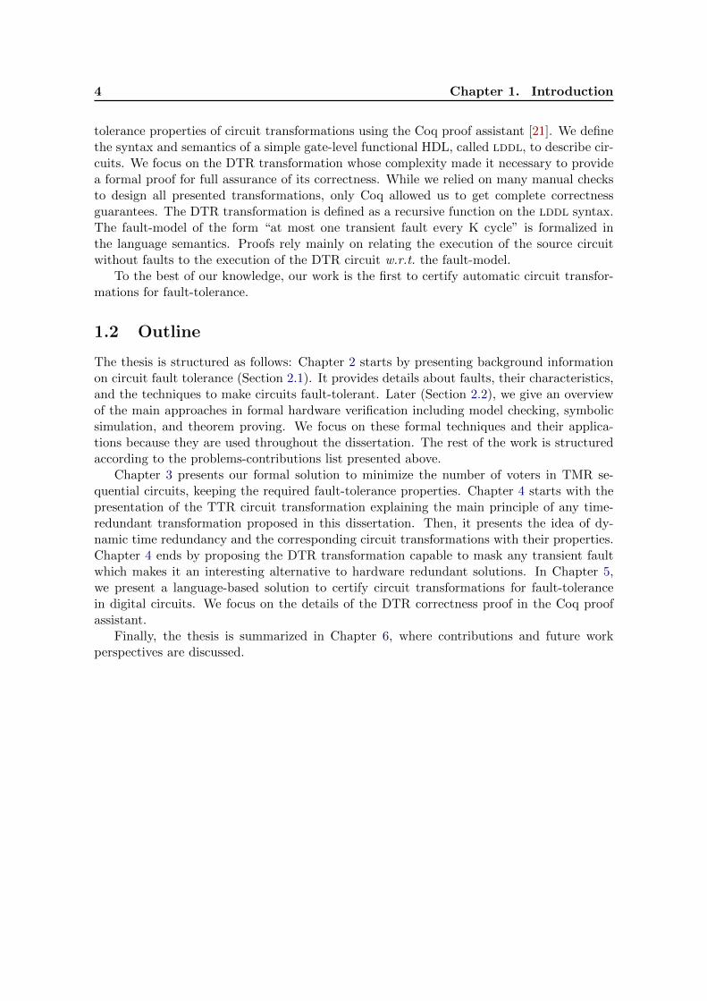
The experiments of TIMA laboratory with 1 Gbit of SRAM memory at 130 nm technol-ogy have shown that 15 soft-errors have been observed during the flight Los Angeles-Paris(23/4/2009) [1]. Among them, there were 5 SEUs and 4 MBUs. It verified the precision ofthe developed prediction tool MUCSA. The dependence between the flight length and thenumber of bit-flips is presented in Figure 2.1.
Figure 2.1: Predicted number of bit-flips vs the number of observed bit-flips [1].
In other experiments in Peru at 3800m, 1 Gbit of SRAM at 90 nm and 130 nm experienced37 bit-flips during 5 months: 10 SEUs and 9 MBUs [1].
Soft-Error Rate (SER) can be as small as 10−5 bit-upset/day for Vertex FPGAs [52] interrestrial conditions.
At geosynchronous Earth orbit altitudes, Lockheed Martin Commercial Space Systemsobserved 1.8x10⁻¹⁰ errors/bit/day in SRAM 0.25µm devices [53]. During solar maximumcondition, SER raised to 1x10⁻⁹ errors/bit/day. MBUs constituted 4-10% of all faults.
Microsemi Corporation [7] lists an extensive list which shows that the radiation-basedsoft-errors are widely observed and already leaded to incidents. Among others, let us cite:
• “In 2008, a Quantas Airbus A330-303 pitched downward twice in rapid succession,diving first 650 feet and then 400 feet. The cause has been traced to errors in an
10 Chapter 2. Circuits Fault-Tolerance and Formal Methods
on-board computer suspected to have been induced by cosmic rays.”
• “Canadian-based St. Jude Medical issued an advisory to doctors in 2005, warning thatSEUs to the memory of its implantable cardiac defibrillators could cause excessive drainon the unit’s battery.” The observed SER in defibrillators was 9.3x10⁻¹² upsets/bit-hour [8].
Due to low fault rates on Earth or even in open space, the most common fault-model isa single fault, e.g., an SEU or an SET. If we relate SER with the number of system clockcycles between two consecutive faults, then we can introduce fault models of the form “atmost n bit-flips within K cycles”, denoted by SEU (n,K), and “at most n SETs within Kcycles”, denoted by SET (n,K).
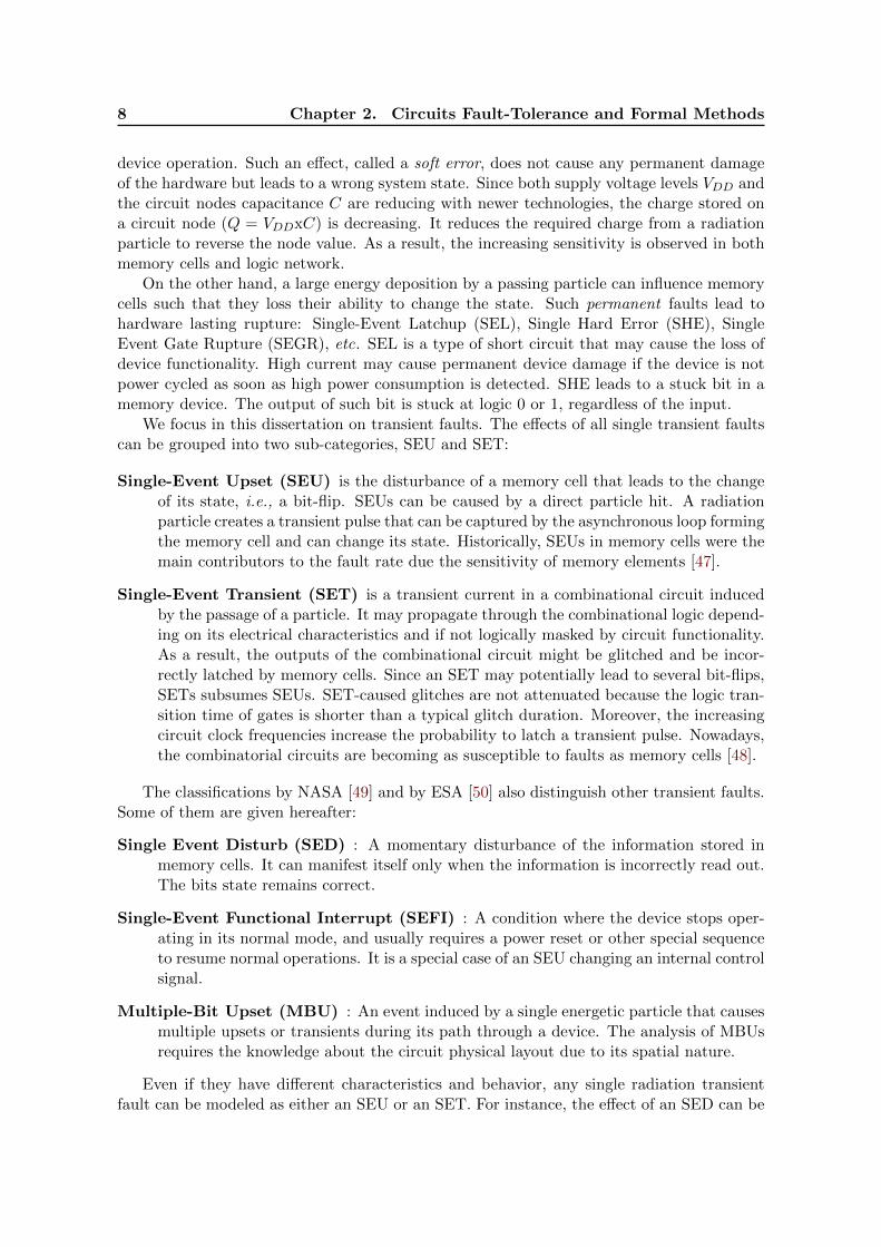
Besides radiation-related faults, it is worth to mention the faults caused by signal metasta-bility during aggressive voltage scaling [2]. Voltage scaling is a technique to reduce circuitenergy demands, it decreases the voltage in the circuit to minimize its power consumption.Figure 2.2 illustrates the dependency between voltage and error rates for an 18x18-bit mul-tiplier at 90MHz in Xilinx XC2V250-F456-5 FPGA.
100.00000000
10.00000000
1.00000000
0.10000000
0.01000000
0.00100000
0.00010000
0.00001000
0.00000100
0.00000010
0.00000001
Erro
rdra
tedp
erce
ntag
ed(l
ogds
cale
)
1.78 1.74 1.70 1.66 1.62 1.58 1.54 1.50 1.46 1.42 1.38 1.34 1.30 1.26 1.22 1.18 1.14
Supplydvoltage
Onederrordeveryd~20dseconds
Figure 2.2: Measured error rates dependency from supply voltage [2]
As it is marked on the plot, when the voltage is 1.52 V, the error rate is one error per 20seconds or per 1.8 billion operations. It corresponds to the fault model SET (1, 1.8x10⁹).
2.1.3 Conventional Fault-Tolerance Techniques
Any fault-tolerance technique is based on some sort of redundancy. There are three redun-dancy classes:
Hardware or spatial redundancy. It adds additional hardware resources to simultane-ously produce several copies of the same computational result for their further com-parison (resp. voting) to detect (resp. to mask) soft-errors. For instance, a duplicatedsystem is capable to detect an error occurrence by comparing the states of its tworedundant modules. The triplicated design can mask an error by majority voting. Ad-ditional hardware introduces the corresponding cost in terms of physical space, power,etc, but it allows avoiding significant performance degradation because redundant com-putations are performed in parallel.
2.1. Circuits Fault Tolerance 11
Time or temporal redundancy. The redundant computations are performed sequentiallymultiple times re-using the same hardware resources. Thus, time redundancy trades-offperformance for a low hardware cost. For instance, if a system re-computes its resulttwice for further comparison, it is capable to detect an error. If the computation istriplicated in time, the system can mask an error by voting on the redundant results.
Information redundancy. It adds extra information (bits) to be used for detection/cor-rection purposes. To operate with and use this information, e.g., parity bits, a systemalso needs additional hardware and/or time resources that encode/decode this extradata.
Furthermore, there is an orthogonal classification of the redundancy types accordingto the system reaction upon error detection and the guarantees on the primary outputscorrectness. In particular:
Active redundancy relies on an error-detection with a subsequent appropriate systemreaction. For example, the system performs a global reset after an error-detection inany of its redundant copies.
Passive redundancy is based on fault-masking techniques to guarantee the correctness ofthe primary outputs. Any fault occurring in the system protected by passive redun-dancy does not change the system output behavior.
Hybrid redundancy incorporates both active and passive types of redundancy.
Since active redundancy does not guarantee the equivalence of output streams with andwithout fault occurrence, it is typically used in systems that can tolerate some temporalservice quality degradation. As the European Space Agency (ESA) states: “In some appli-cations it is sufficient to detect an error caused by an SEU and to flag the affected data asinvalid or corrupted” [49].
The two observed classifications are orthogonal. There are systems where an error detec-tion of active redundancy is realized through hardware duplication with comparison (hard-ware redundancy), error detection codes (information redundancy), or self-checking logic(time redundancy) [31].
The next three sections present hardware, time, and information redundancies in details.
2.1.3.1 Hardware Redundancy
The lectures by von Neumann given in Princeton University in 1952 [54] can be consideredas the first theoretical work about hardware redundancy. He proposed and analyzed Triple-Modular Redundancy (TMR) that stays to be the most popular approach for error maskingin safety-critical applications.
TMR relies on three redundant copies of an original system receiving the same inputs.Majority voters are introduced at the primary triplicated outputs. If at least two of three re-dundant outputs return correct values, the voters return the correct result, therefore maskingone possible error. TMR is able to detect one or two errors and to correct one.
Double Modular Redundancy (DMR) represents the reduced version of TMR that hasonly two redundant modules and is only capable to detect one error. The generalized versionof TMR, called N-modular redundancy, requires N redundant copies of a system to feedmajority voters with N inputs. It can correct bN−1
2 c errors and detect (N − 1) errors.There are several versions of TMR that can be applied to circuits [12], in particular:
12 Chapter 2. Circuits Fault-Tolerance and Formal Methods
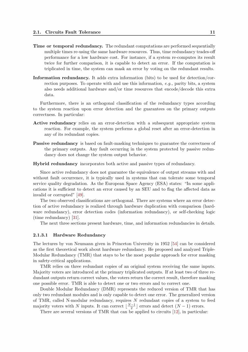
1. the whole circuit triplication with the insertion of a single majority voter at eachprimary output (as in the von Neumann’s original TMR);
2. only memory cells are triplicated with a single voter after each triplicated cell and eachprimary output;
3. the whole circuit triplication with a single voter after each triplicated memory cell andeach triplicated primary output;
4. the whole circuit triplication with three voters after each triplicated memory cell andeach triplicated primary output.
The first TMR version, depicted in Figure 2.3, is tolerant only to a single fault, temporalor permanent, occurring inside one of the redundant modules. When a fault occurs in amodule, its state becomes corrupted and may stay erroneous forever if it does not haveany additional error-masking mechanisms. This is why this scheme is tolerant only to asingle internal fault of the modules. This TMR version may not be capable to tolerate asecond fault occurring in a different module. If another fault occurs (even long after thefirst one) and corrupts the second module, the TMR structure would have two erroneousmodules simultaneously and cannot guarantee anymore the correctness of primary outputs.Furthermore, if an SET corrupts an output voter, then the correctness of the output is notguaranteed. As a result, the first TMR modification is tolerant to the fault models (notationsof Section 2.1.2.1): SEU(1,∞) and SET (1,∞), provided that faults do not occur at theoutput voters.
Module
Module
Module
Input
Figure 2.3: TMR scheme proposed by von Neumann.
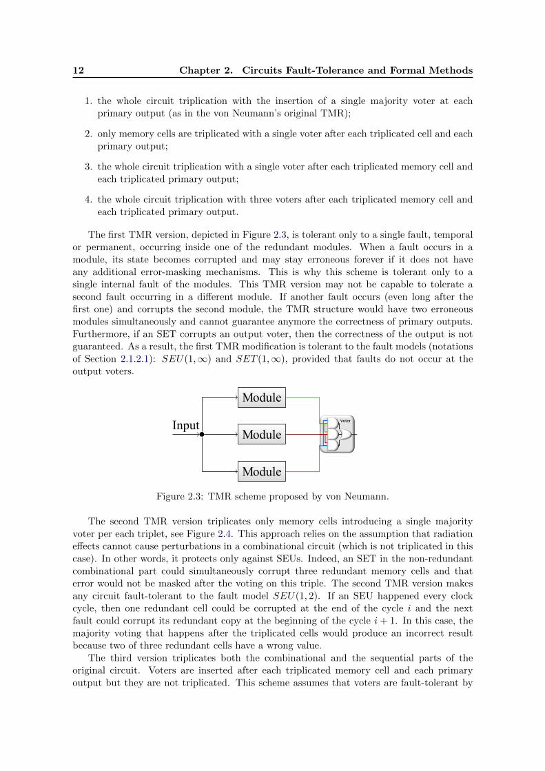
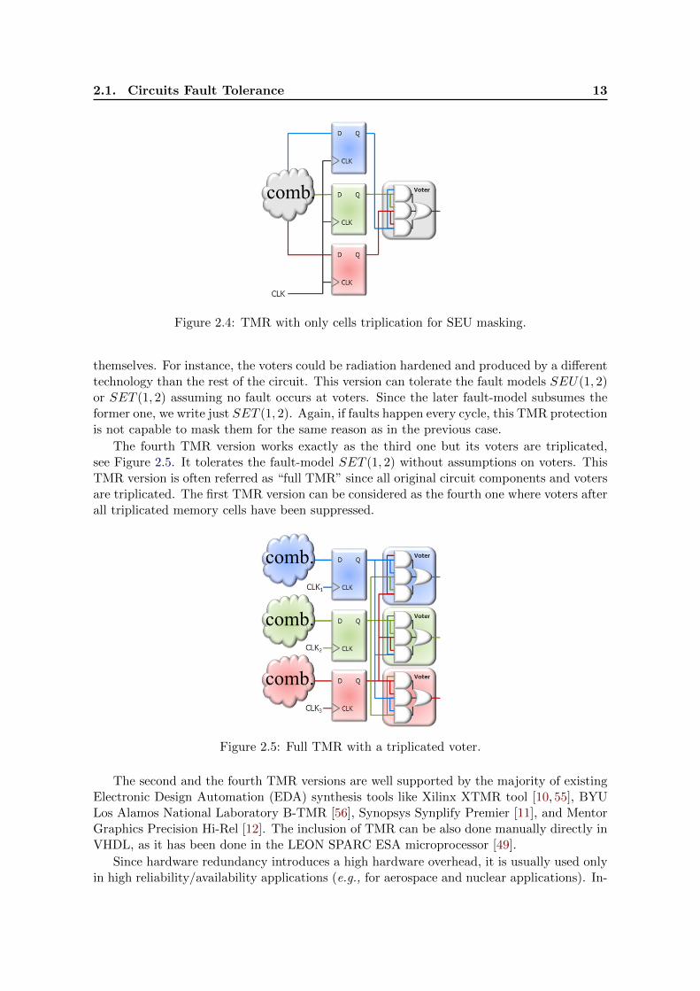
The second TMR version triplicates only memory cells introducing a single majorityvoter per each triplet, see Figure 2.4. This approach relies on the assumption that radiationeffects cannot cause perturbations in a combinational circuit (which is not triplicated in thiscase). In other words, it protects only against SEUs. Indeed, an SET in the non-redundantcombinational part could simultaneously corrupt three redundant memory cells and thaterror would not be masked after the voting on this triple. The second TMR version makesany circuit fault-tolerant to the fault model SEU(1, 2). If an SEU happened every clockcycle, then one redundant cell could be corrupted at the end of the cycle i and the nextfault could corrupt its redundant copy at the beginning of the cycle i+ 1. In this case, themajority voting that happens after the triplicated cells would produce an incorrect resultbecause two of three redundant cells have a wrong value.
The third version triplicates both the combinational and the sequential parts of theoriginal circuit. Voters are inserted after each triplicated memory cell and each primaryoutput but they are not triplicated. This scheme assumes that voters are fault-tolerant by
2.1. Circuits Fault Tolerance 13
comb.
Figure 2.4: TMR with only cells triplication for SEU masking.
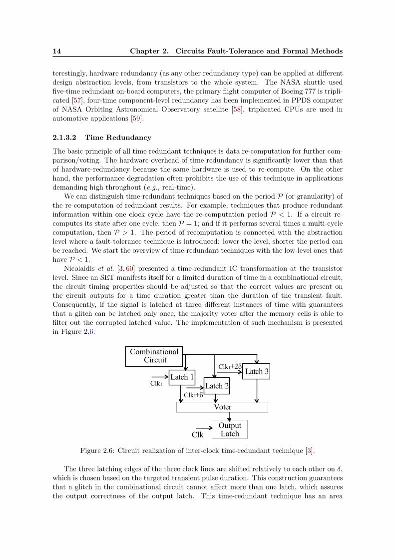
themselves. For instance, the voters could be radiation hardened and produced by a differenttechnology than the rest of the circuit. This version can tolerate the fault models SEU(1, 2)or SET (1, 2) assuming no fault occurs at voters. Since the later fault-model subsumes theformer one, we write just SET (1, 2). Again, if faults happen every cycle, this TMR protectionis not capable to mask them for the same reason as in the previous case.
The fourth TMR version works exactly as the third one but its voters are triplicated,see Figure 2.5. It tolerates the fault-model SET (1, 2) without assumptions on voters. ThisTMR version is often referred as “full TMR” since all original circuit components and votersare triplicated. The first TMR version can be considered as the fourth one where voters afterall triplicated memory cells have been suppressed.
comb.
comb.
comb.
Figure 2.5: Full TMR with a triplicated voter.
The second and the fourth TMR versions are well supported by the majority of existingElectronic Design Automation (EDA) synthesis tools like Xilinx XTMR tool [10, 55], BYULos Alamos National Laboratory B-TMR [56], Synopsys Synplify Premier [11], and MentorGraphics Precision Hi-Rel [12]. The inclusion of TMR can be also done manually directly inVHDL, as it has been done in the LEON SPARC ESA microprocessor [49].
Since hardware redundancy introduces a high hardware overhead, it is usually used onlyin high reliability/availability applications (e.g., for aerospace and nuclear applications). In-
14 Chapter 2. Circuits Fault-Tolerance and Formal Methods
terestingly, hardware redundancy (as any other redundancy type) can be applied at differentdesign abstraction levels, from transistors to the whole system. The NASA shuttle usedfive-time redundant on-board computers, the primary flight computer of Boeing 777 is tripli-cated [57], four-time component-level redundancy has been implemented in PPDS computerof NASA Orbiting Astronomical Observatory satellite [58], triplicated CPUs are used inautomotive applications [59].
2.1.3.2 Time Redundancy
The basic principle of all time redundant techniques is data re-computation for further com-parison/voting. The hardware overhead of time redundancy is significantly lower than thatof hardware-redundancy because the same hardware is used to re-compute. On the otherhand, the performance degradation often prohibits the use of this technique in applicationsdemanding high throughout (e.g., real-time).
We can distinguish time-redundant techniques based on the period P (or granularity) ofthe re-computation of redundant results. For example, techniques that produce redundantinformation within one clock cycle have the re-computation period P < 1. If a circuit re-computes its state after one cycle, then P = 1; and if it performs several times a multi-cyclecomputation, then P > 1. The period of recomputation is connected with the abstractionlevel where a fault-tolerance technique is introduced: lower the level, shorter the period canbe reached. We start the overview of time-redundant techniques with the low-level ones thathave P < 1.
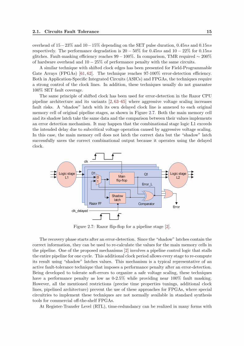
Nicolaidis et al. [3, 60] presented a time-redundant IC transformation at the transistorlevel. Since an SET manifests itself for a limited duration of time in a combinational circuit,the circuit timing properties should be adjusted so that the correct values are present onthe circuit outputs for a time duration greater than the duration of the transient fault.Consequently, if the signal is latched at three different instances of time with guaranteesthat a glitch can be latched only once, the majority voter after the memory cells is able tofilter out the corrupted latched value. The implementation of such mechanism is presentedin Figure 2.6.
Clk1 Latch 2Latch 1
Latch 3
Voter
Clk
Combinational Circuit
Output Latch
Clk1
Clk1
+δ
+2δ
Figure 2.6: Circuit realization of inter-clock time-redundant technique [3].
The three latching edges of the three clock lines are shifted relatively to each other on δ,which is chosen based on the targeted transient pulse duration. This construction guaranteesthat a glitch in the combinational circuit cannot affect more than one latch, which assuresthe output correctness of the output latch. This time-redundant technique has an area
2.1. Circuits Fault Tolerance 15
overhead of 15−23% and 10−15% depending on the SET pulse duration, 0.45ns and 0.15nsrespectively. The performance degradation is 20− 50% for 0.45ns and 10− 22% for 0.15nsglitches. Fault-masking efficiency reaches 99− 100%. In comparison, TMR required ∼ 200%of hardware overhead and 10− 25% of performance penalty with the same circuits.
A similar technique with shifted clock edges has been presented for Field-ProgrammableGate Arrays (FPGAs) [61, 62]. The technique reaches 97-100% error-detection efficiency.Both in Application-Specific Integrated Circuits (ASICs) and FPGAs, the techniques requirea strong control of the clock lines. In addition, these techniques usually do not guarantee100% SET fault coverage.
The same principle of shifted clock has been used for error-detection in the Razor CPUpipeline architecture and its variants [2, 63–65] where aggressive voltage scaling increasesfault risks. A “shadow” latch with its own delayed clock line is annexed to each originalmemory cell of original pipeline stages, as shown in Figure 2.7. Both the main memory celland its shadow latch take the same data and the comparison between their values implementsan error detection mechanism. It may happen that the combinational stage logic L1 exceedsthe intended delay due to subcritical voltage operation caused by aggressive voltage scaling.In this case, the main memory cell does not latch the correct data but the “shadow” latchsuccessfully saves the correct combinational output because it operates using the delayedclock.
RazorkFF
01
LogickstageL2Main
flip-flop
Shadowlatch
Error_L
ErrorComparator
clk
clk_delayed
Q1D1LogickstageL1
Figure 2.7: Razor flip-flop for a pipeline stage [2].
The recovery phase starts after an error-detection. Since the “shadow” latches contain thecorrect information, they can be used to re-calculate the values for the main memory cells inthe pipeline. One of the proposed mechanisms [2] involves a pipeline control logic that stallsthe entire pipeline for one cycle. This additional clock period allows every stage to re-computeits result using “shadow” latches values. This mechanism is a typical representative of anactive fault-tolerance technique that imposes a performance penalty after an error-detection.Being developed to tolerate soft-errors to organize a safe voltage scaling, these techniqueshave a performance penalty as low as 0-2.5% while providing near 100% fault masking.However, all the mentioned restrictions (precise time properties tunings, additional clocklines, pipelined architecture) prevent the use of these approaches for FPGAs, where specialcircuitries to implement these techniques are not normally available in standard synthesistools for commercial off-the-shelf FPGAs.
At Register-Transfer Level (RTL), time-redundancy can be realized in many forms with
16 Chapter 2. Circuits Fault-Tolerance and Formal Methods
different periods of re-computation. For instance, let us assume that an original circuitcomputes and returns the result during n clock cycles (a block of information). Its triple-time redundant version with P = n works according to the next three-step scenario:
1. It fully computes and stores the result a first time. It takes n cycles.
2. It re-computes and stores the result a second time. It takes another n cycles.
3. Finally, it re-computes and stores the result a third time, again during n cycles.
With three independently calculated outputs, a corruption of any of them can be masked byvoting. This approach is similar to software fault-tolerance techniques where a program isre-executed three times to produce three independent redundant computation results.
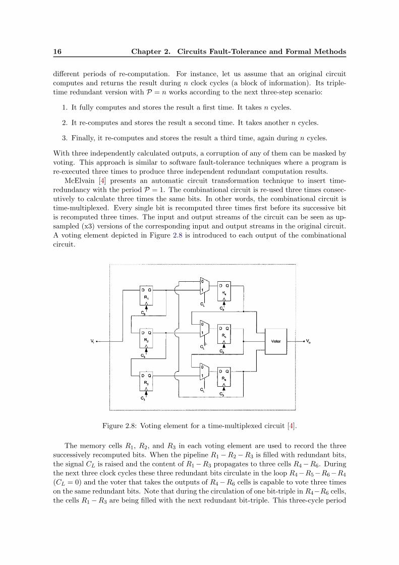
McElvain [4] presents an automatic circuit transformation technique to insert time-redundancy with the period P = 1. The combinational circuit is re-used three times consec-utively to calculate three times the same bits. In other words, the combinational circuit istime-multiplexed. Every single bit is recomputed three times first before its successive bitis recomputed three times. The input and output streams of the circuit can be seen as up-sampled (x3) versions of the corresponding input and output streams in the original circuit.A voting element depicted in Figure 2.8 is introduced to each output of the combinationalcircuit.
Figure 2.8: Voting element for a time-multiplexed circuit [4].
The memory cells R1, R2, and R3 in each voting element are used to record the threesuccessively recomputed bits. When the pipeline R1−R2−R3 is filled with redundant bits,the signal CL is raised and the content of R1−R3 propagates to three cells R4−R6. Duringthe next three clock cycles these three redundant bits circulate in the loop R4−R5−R6−R4
(CL = 0) and the voter that takes the outputs of R4−R6 cells is capable to vote three timeson the same redundant bits. Note that during the circulation of one bit-triple in R4−R6 cells,the cells R1−R3 are being filled with the next redundant bit-triple. This three-cycle period

2.1. Circuits Fault Tolerance 17
repeats. As a result, the output of a voting element is error-free even if the combinationalpart experiences an SET.
We can notice that there is a single point of failure in this voting element (Figure 2.8):if the signal CL is corrupted by an SET, it may corrupt two or even three cells R4−R6 thatcontain redundant information. In this case, the voter cannot mask an error.
Since each input and output is triplicated in time when the period P = 1, this fault-tolerant scheme can be considered as stream-oriented. This scheme is a typical representa-tive of passive fault-tolerance techniques where error masking does not require a dedicatedrecovery process.
As an active fault-tolerance technique, we can consider schemes based on checkpointingand rollback. The circuit state (the content of its memory cells) is saved periodically andre-stored after an error detection. The circuit rolls-back to its previous correct state andre-computes the results previously computed. Since it relies on re-computation, this groupof techniques can be also considered as time-redundant. Thus, the Razor architecture imple-ments an active fault-tolerance technique with “shadow” latches keeping the circuit correctstate.
Carven Chan et al. [66] show how checkpointing/rollback mechanisms can be automat-ically inserted at register-transfer level. The used Backwards Error Recovery (BER) takessnapshots of the system states and after an error detection rolls back within one clock cycle.Until this work, BER had been implemented only manually, e.g., for processors [67,68]. Us-ing syntactic additions to standard Verilog HDL, the main circuit design is separated fromthe BER mechanism. The approach requires minimal modifications of an original Verilogdesign. A user must choose which signals to checkpoint, the conditions when their valuesare saved, the error-detection conditions when the states are restored, etc. All these cir-cuit fault-tolerance actions are described as guarded operations [69] on the original circuitdesign. While flexibility and generality of this automatic approach makes it applicable toalmost all cases where checkpointing/rollback are needed, the user-defined error-detectioncondition in the form of assertions does not guarantee to take into account all possible tran-sient fault effects. It has not been investigated if a transient fault can corrupt simultaneouslyboth a circuit and its checkpointed snapshot. If such possibility exists, the rollback may beperformed to a wrong state. Therefore, its flexibility requires a deep understanding of theoriginal circuit to make the proper decisions about checkpointing and rollback conditions.Similar approaches have been proposed in [70] with multi-cycles rollback from a register fileand in [14] at a gate-level.
General hardware checkpointing/rollback techniques have also been proposed as micro-architectural transformations [14]. However, the resulting circuit is tolerant to SEUs butnot to SETs. Indeed, an SET may corrupt both a cell (i.e., the current state) and its copy(i.e., its checkpoint) because they use the same input data signal that can be glitched bythe same SET. As a result, when an error is detected, the rollback may return the circuit toan incorrect state.
The checkpointing/rollback mechanisms allow the system to reduce the performancepenalty introduced by time-redundancy. Instead of triple-time redundancy a system canuse a double-time redundant scheme with checkpointing/rollback to mask an error. As aresult, the throughput loss can be reduced from triple to double one but the system ob-tains the same fault-tolerance properties. In general, the recovery (rollback and a thirdre-computation) disturbs the output stream and is not transparent to the surrounding cir-cuit.
18 Chapter 2. Circuits Fault-Tolerance and Formal Methods
Besides performance penalty, another disadvantage of time-redundancy is that it does notmask a permanent fault because all redundant results computed on a permanently corruptedhardware will be wrong. In comparison, a single permanent fault in TMR does not lead toerroneous results since only one redundant module is out of order. TMR will however stopworking upon the next fault (even transient) happening in another redundant module thanthe permanently corrupted one. Nevertheless, there are mixed forms of time redundancy withinput data encoding (and an additional hardware cost) that are capable of detecting the effectof a permanent fault. One of them is alternating logic [71] that achieves error detection usingtime redundancy. The original combinational circuit is modified to implement a self-dualfunction. The first cycle, the signals propagate through the combinational circuit and itsoutputs are saved. The second cycle, an inverted version of the same signals is given to thecombinational circuit. Comparing these two results, a circuit can detect a fault.
2.1.3.3 Information Redundancy
Information redundancy adds extra bits to data, often using encoding, and uses this extra in-formation for error-detection and error-correction. The most common circuit fault-tolerancetechniques that use information redundancy are FSM encoding and memory encoding usingError-Correcting Codes (ECC).
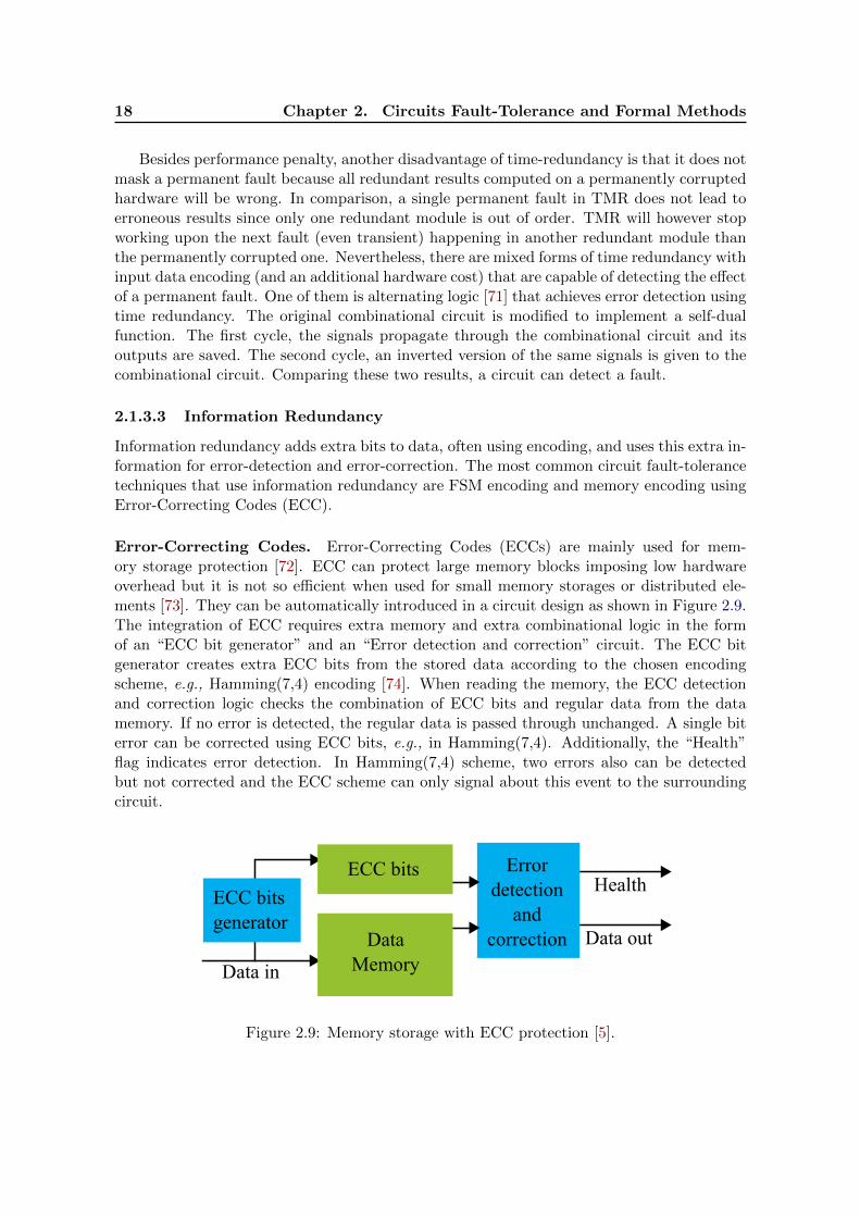
Error-Correcting Codes. Error-Correcting Codes (ECCs) are mainly used for mem-ory storage protection [72]. ECC can protect large memory blocks imposing low hardwareoverhead but it is not so efficient when used for small memory storages or distributed ele-ments [73]. They can be automatically introduced in a circuit design as shown in Figure 2.9.The integration of ECC requires extra memory and extra combinational logic in the formof an “ECC bit generator” and an “Error detection and correction” circuit. The ECC bitgenerator creates extra ECC bits from the stored data according to the chosen encodingscheme, e.g., Hamming(7,4) encoding [74]. When reading the memory, the ECC detectionand correction logic checks the combination of ECC bits and regular data from the datamemory. If no error is detected, the regular data is passed through unchanged. A single biterror can be corrected using ECC bits, e.g., in Hamming(7,4). Additionally, the “Health”flag indicates error detection. In Hamming(7,4) scheme, two errors also can be detectedbut not corrected and the ECC scheme can only signal about this event to the surroundingcircuit.
Data out
HealthECC bits
ECC bitsgenerator
Data in
DataMemory
Errordetection
andcorrection
Figure 2.9: Memory storage with ECC protection [5].
2.1. Circuits Fault Tolerance 19
Table 2.1.3: Hamming code (7,4).
1 2 3 4 5 6 7Data p0 p1 u3 p2 u2 u1 u0
0 0 0 0 0 0 0 01 1 1 0 1 0 0 12 0 1 0 1 0 1 03 1 0 0 0 0 1 14 1 0 0 1 1 0 05 0 1 0 0 1 0 16 1 1 0 0 1 1 0...13 1 0 1 0 1 0 114 0 0 1 0 1 1 015 1 1 1 1 1 1 1
Historically, ECC has been introduced due to the high soft error rate in large memorybanks. However, it introduces resilience against other fault types, e.g., a permanent fault ina single bit (a stuck bit).
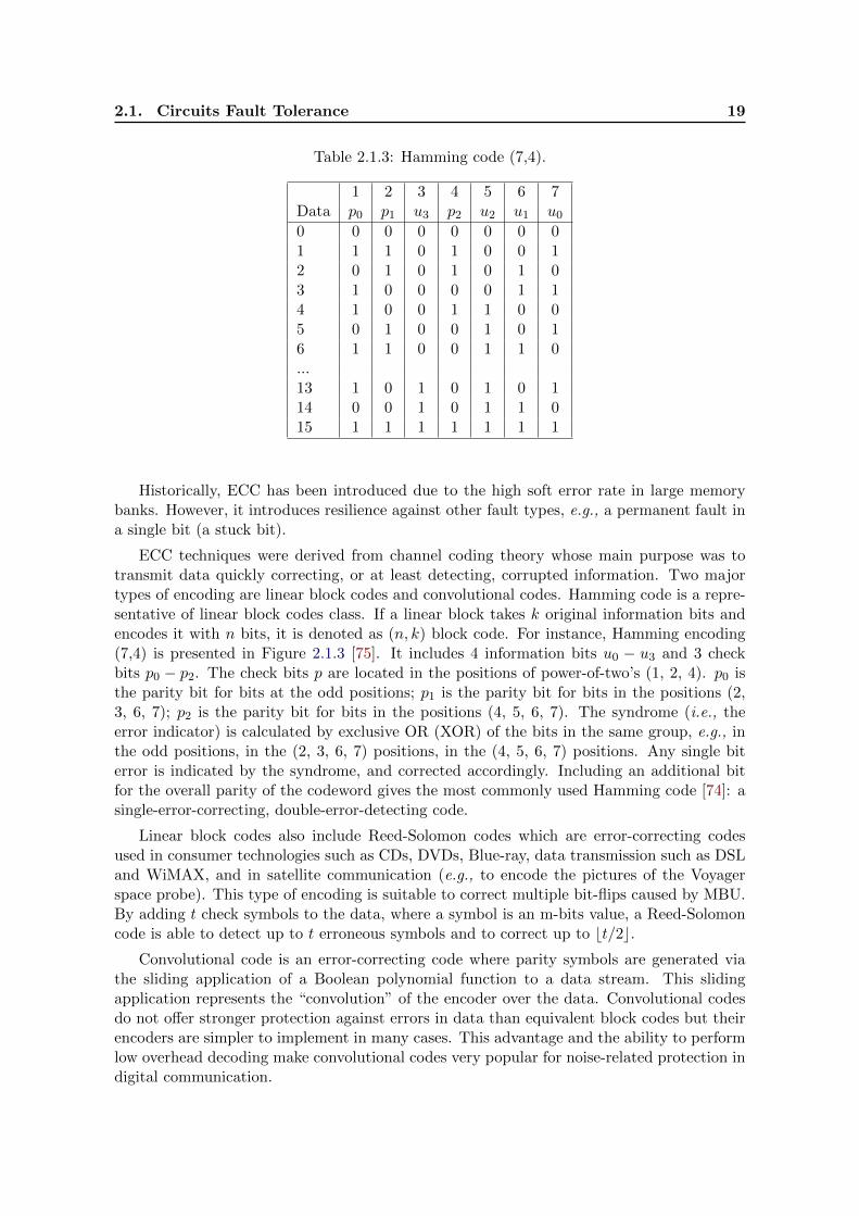
ECC techniques were derived from channel coding theory whose main purpose was totransmit data quickly correcting, or at least detecting, corrupted information. Two majortypes of encoding are linear block codes and convolutional codes. Hamming code is a repre-sentative of linear block codes class. If a linear block takes k original information bits andencodes it with n bits, it is denoted as (n, k) block code. For instance, Hamming encoding(7,4) is presented in Figure 2.1.3 [75]. It includes 4 information bits u0 − u3 and 3 checkbits p0 − p2. The check bits p are located in the positions of power-of-two’s (1, 2, 4). p0 isthe parity bit for bits at the odd positions; p1 is the parity bit for bits in the positions (2,3, 6, 7); p2 is the parity bit for bits in the positions (4, 5, 6, 7). The syndrome (i.e., theerror indicator) is calculated by exclusive OR (XOR) of the bits in the same group, e.g., inthe odd positions, in the (2, 3, 6, 7) positions, in the (4, 5, 6, 7) positions. Any single biterror is indicated by the syndrome, and corrected accordingly. Including an additional bitfor the overall parity of the codeword gives the most commonly used Hamming code [74]: asingle-error-correcting, double-error-detecting code.
Linear block codes also include Reed-Solomon codes which are error-correcting codesused in consumer technologies such as CDs, DVDs, Blue-ray, data transmission such as DSLand WiMAX, and in satellite communication (e.g., to encode the pictures of the Voyagerspace probe). This type of encoding is suitable to correct multiple bit-flips caused by MBU.By adding t check symbols to the data, where a symbol is an m-bits value, a Reed-Solomoncode is able to detect up to t erroneous symbols and to correct up to bt/2c.
Convolutional code is an error-correcting code where parity symbols are generated viathe sliding application of a Boolean polynomial function to a data stream. This slidingapplication represents the “convolution” of the encoder over the data. Convolutional codesdo not offer stronger protection against errors in data than equivalent block codes but theirencoders are simpler to implement in many cases. This advantage and the ability to performlow overhead decoding make convolutional codes very popular for noise-related protection indigital communication.
20 Chapter 2. Circuits Fault-Tolerance and Formal Methods
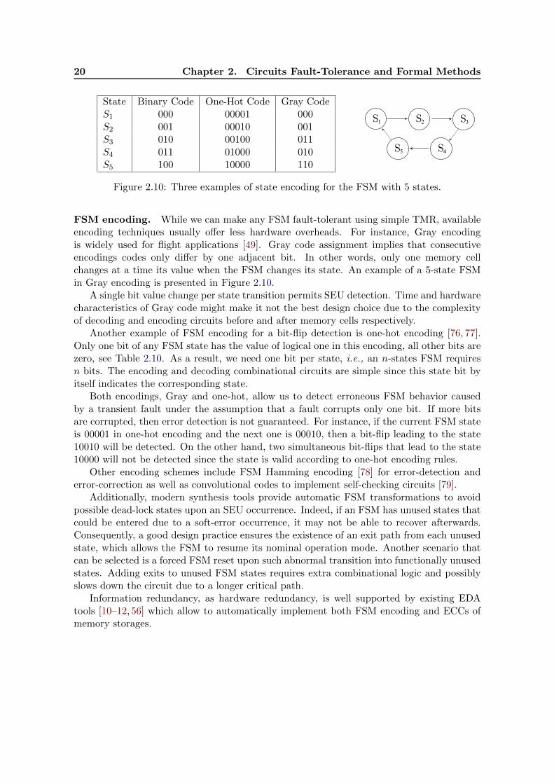
State Binary Code One-Hot Code Gray CodeS1 000 00001 000S2 001 00010 001S3 010 00100 011S4 011 01000 010S5 100 10000 110
S1 S3S4S5
S2
Figure 2.10: Three examples of state encoding for the FSM with 5 states.
FSM encoding. While we can make any FSM fault-tolerant using simple TMR, availableencoding techniques usually offer less hardware overheads. For instance, Gray encodingis widely used for flight applications [49]. Gray code assignment implies that consecutiveencodings codes only differ by one adjacent bit. In other words, only one memory cellchanges at a time its value when the FSM changes its state. An example of a 5-state FSMin Gray encoding is presented in Figure 2.10.
A single bit value change per state transition permits SEU detection. Time and hardwarecharacteristics of Gray code might make it not the best design choice due to the complexityof decoding and encoding circuits before and after memory cells respectively.
Another example of FSM encoding for a bit-flip detection is one-hot encoding [76, 77].Only one bit of any FSM state has the value of logical one in this encoding, all other bits arezero, see Table 2.10. As a result, we need one bit per state, i.e., an n-states FSM requiresn bits. The encoding and decoding combinational circuits are simple since this state bit byitself indicates the corresponding state.
Both encodings, Gray and one-hot, allow us to detect erroneous FSM behavior causedby a transient fault under the assumption that a fault corrupts only one bit. If more bitsare corrupted, then error detection is not guaranteed. For instance, if the current FSM stateis 00001 in one-hot encoding and the next one is 00010, then a bit-flip leading to the state10010 will be detected. On the other hand, two simultaneous bit-flips that lead to the state10000 will not be detected since the state is valid according to one-hot encoding rules.
Other encoding schemes include FSM Hamming encoding [78] for error-detection anderror-correction as well as convolutional codes to implement self-checking circuits [79].
Additionally, modern synthesis tools provide automatic FSM transformations to avoidpossible dead-lock states upon an SEU occurrence. Indeed, if an FSM has unused states thatcould be entered due to a soft-error occurrence, it may not be able to recover afterwards.Consequently, a good design practice ensures the existence of an exit path from each unusedstate, which allows the FSM to resume its nominal operation mode. Another scenario thatcan be selected is a forced FSM reset upon such abnormal transition into functionally unusedstates. Adding exits to unused FSM states requires extra combinational logic and possiblyslows down the circuit due to a longer critical path.
Information redundancy, as hardware redundancy, is well supported by existing EDAtools [10–12, 56] which allow to automatically implement both FSM encoding and ECCs ofmemory storages.

2.2. Formal Methods in Circuit Design 21
2.2 Formal Methods in Circuit Design
The high complexity of a modern circuit makes mandatory the verification of its designcorrectness since the confidence in the design cannot be anymore obtained through simplecircuit simulations. It is necessary to catch all design errors as early as possible to minimizethe re-design cost and to reduce time-to-market. Formal methods can replace simulation-based verification giving full assurance that the implementation satisfies a given specification.The term implementation refers to the circuit design to be verified and the term specificationdesignates the property that defines the correctness [80].
“Formal methods are system design techniques that use rigorously specified mathematicalmodels to build software and hardware systems” [81,82]. Using formal methods, engineers areable to specify the system behavior, to implement the design, as well as to verify particularproperties of the implementation.
There is a distinction between design verification (or validation) and implementationverification. The former checks the design specification correctness relatively to the originaldesign requirements and aspects. In other words, it checks the correspondence of the specifi-cation w.r.t. the required pre-defined properties (e.g., deadlock freedom). The latter verifiesthe design steps correctness and the correspondence between circuit models before and afterrefinements (e.g., before and after optimization steps during circuit synthesis).
Different design abstraction levels dictate their own formal representations, e.g., gatesnetlists, FSMs, data flow graphs. At the same time, the specifications and properties canbe expressed in terms of logic (e.g., propositional logic, µ-calculus) or automata/languagetheory (e.g., ω-automata).
Using formal methods, the correctness of every refinement step from high algorithmicbehavioral abstraction level to its low hardware realization can be proved. However, thecomplexity and the time needed make such complete verification impractical in the majorityof cases. One exception is safety-critical (aerospace, defense, etc) applications [83,84] wherethe cost and consequences of erroneous behavior prevail the cost of verification.
Gupta gave a classification of formal methods [80] grouping them in four categories:
• Model Checking is an automated verification technique that checks if a system, encodedusually in the form of finite-state model, satisfies a specification given in the form of alogic formula.
• Theorem proving expresses the relationship between the design implementation and itsspecification as a formal statement that has to be proven. The validity of the statementis established in a proof assistant using axioms and implementation assumptions. Whileproof assistants facilitate and certify proof procedures, theorem proving is mainly amanual technique.
• Equivalence Checking is an automatic approach to show the equivalence between aspecification and an implementation (e.g., FSM equivalence, equivalence between func-tions). This technique is widely used to show the equivalence between an RTL circuitdescription and its synthesized netlist before and after optimizations.
• Language containment is a technique checking correctness by showing that the languageof an implementation is contained in the language of a specification. Both design andproperty are expressed as FSMs/automata. Then, the property is complemented andcomposed into the design to form the product of the two FSMs. The language emptinessis checked by traversing the product.
22 Chapter 2. Circuits Fault-Tolerance and Formal Methods
The research presented in this dissertation mainly relies on the first two groups of formalmethods that are discussed in details below. Other surveys presenting formal methods inhardware can be found in [85–88].
2.2.1 Model Checking
Model checking [89–91] is an automated verification technique for checking if a system,usually described as a finite-state model, has designated properties expressed as a temporallogic formula [90]. A model checker exhaustively examines all behaviors of the given systemto confirm its correctness or to provide a counterexample if the property is violated. Forinstance, it can be used to prove that an interrupt in a circuit is acknowledged at most tclock cycles after the interrupt request.
A property can be expressed in propositional logic and some of its extensions. Proposi-tional logic by itself deals with absolute truths in a domain and is usually used to expressstate properties. One of the extensions of propositional logic is propositional temporal logicthat has temporal modalities [92] . The underlying nature of time divides temporal logicsinto two categories: linear and branching. In linear logics (e.g., LTL [90]), there is a singlesuccessor moment for each moment in time. In branching logics (e.g., CTL [93]), each mo-ment has a branching tree-like structure, where scenarios may split into alternative courses.For instance, if a path ~pi = s0, s1, ... is a possible sequence of system states, then a propertyformula in LTL is Af where f is a path formula. A system satisfies an LTL property Af ifall state paths of the system satisfy f . If there is a path not satisfying f , this path definesa counterexample. One of the ways to check an LTL property is to express the model andthe negation of the property as Non-deterministic Buchi Automata (NBA). Their emptyintersection signifies that the model satisfies the property.
Since model checking technique relies on exhaustive checking, its limitation is the statespace explosion that happens when a system state space is too large to be processed. Average-size circuits have often a huge state space and space explosion can impose prohibitive memoryand time processing requirements. Significant research efforts have been put to increasemodel checking scalability. We shortly observe the main model checking techniques below.
The first breakthrough in model checking scalability was introduced with Binary-DecisionDiagrams (BDDs) [94] that offered a compact way to represent binary functions and statespaces. Symbolic model checking [95] is built on BDD structures and increased the scalabilityfrom dozens to a few hundred memory cells. The name of the technique comes from the factthat finite state models are not stored explicitly, but expressed through BDDs [96]. We givemore details about that approach in the next section.
Another improvement step in scalability was the introduction of bounded model check-ing [97] which was mainly aimed at finding counterexamples or design errors in a system im-plementation. Its basic idea is to search for a counterexample in system executions boundedby some k execution steps. It either finds a counterexample path of length k or less, orconcludes that the property cannot be assured. This problem can be efficiently reduced to apropositional satisfiability problem, and be solved by SAT methods rather than BDDs [98].SAT-based techniques do not suffer from the space explosion problem and they can handlehundreds of thousands of variables nowadays. The main drawback of the bounded modelchecking approach is its incompleteness, it cannot guarantee that there is no counterexamplepath of size greater than k. Completeness can be obtained when the length of the longestpath is shorter than k, but it is hard to compute the proper bound k for termination.
SAT-based unbounded model checking has also been proposed for full verification. It
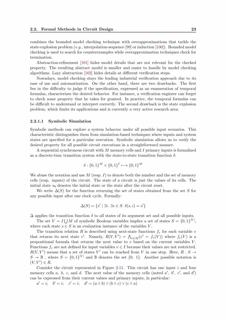
2.2. Formal Methods in Circuit Design 23
combines the bounded model checking technique with overapproximations that tackle thestate-explosion problem (e.g., interpolation-sequence [99] or induction [100]). Bounded modelchecking is used to search for counterexamples while overapproximation techniques check fortermination.
Abstraction-refinement [101] hides model details that are not relevant for the checkedproperty. The resulting abstract model is smaller and easier to handle by model checkingalgorithms. Lazy abstraction [102] hides details at different verification steps.
Nowadays, model checking stays the leading industrial verification approach due to itsease of use and automatization. On the other hand, there are two drawbacks. The firstlies in the difficulty to judge if the specification, expressed as an enumeration of temporalformulas, characterizes the desired behavior. For instance, a verification engineer can forgetto check some property that he takes for granted. In practice, the temporal formulas canbe difficult to understand or interpret correctly. The second drawback is the state explosionproblem, which limits its applications and is currently a very active research area.
2.2.1.1 Symbolic Simulation
Symbolic methods can explore a system behavior under all possible input scenarios. Thischaracteristic distinguishes them from simulation-based techniques where inputs and systemstates are specified for a particular execution. Symbolic simulation allows us to verify thedesired property for all possible circuit executions in a straightforward manner.
A sequential synchronous circuit with M memory cells and I primary inputs is formalizedas a discrete-time transition system with the state-to-state transition function δ:
δ : {0, 1}M × {0, 1}I 7−→ {0, 1}M
We abuse the notation and use M (resp. I) to denote both the number and the set of memorycells (resp. inputs) of the circuit. The state of a circuit is just the values of its cells. Theinitial state s0 denotes the initial state or the state after the circuit reset.
We write ∆(S) for the function returning the set of states obtained from the set S forany possible input after one clock cycle. Formally:
∆(S) = {s′ | ∃i. ∃s ∈ S. δ(s, i) = s′}
∆ applies the transition function δ to all states of its argument set and all possible inputs.
The set V = I⋃M of symbolic Boolean variables implies a set of states S = {0, 1}|V |,
where each state s ∈ S is an evaluation instance of the variables V .
The transition relation R is described using next-state functions fv for each variable vthat returns its next state v′. Namely, R(V, V ′) =
∧v∈M (v′ = fv(V )) where fv(V ) is a
propositional formula that returns the next value to v based on the current variables V .Functions fv are not defined for input variables v ∈ I because their values are not restricted.R(V, V ′) means that a set of states V ′ can be reached from V in one step. Here, R : S →S → B , where S = {0, 1}|V | and B denotes the set {0, 1}. Another possible notation is(V, V ′) ∈ R.
Consider the circuit represented in Figure 2.11. This circuit has one input i and fourmemory cells a, b, c, and d. The next value of the memory cells (noted a′, b′, c′, and d′)can be expressed from their current values and primary inputs, in particular:
a′ = i; b′ = i; c′ = i; d′ = (a ∧ b) ∨ (b ∧ c) ∨ (c ∧ a)

24 Chapter 2. Circuits Fault-Tolerance and Formal Methods
i ba
dc
Figure 2.11: Circuit with a majority voter.
The circuit states are the Boolean tuple (a, b, c, d). The next state transition functionδ : {0, 1}4 × {0, 1}1 7−→ {0, 1}4 can be expressed as:
δ((a, b, c, d), i) = (i, i, i, (a ∧ b) ∨ (b ∧ c) ∨ (c ∧ a))
The corresponding transition relation function is:
R(i, a, b, c, d)(i′, a′, b′, c′, d′) = (a′ = i) ∧ (b′ = i) ∧ (c′ = i) ∧ (d′ = (a ∧ b) ∨ (b ∧ c) ∨ (c ∧ a))
A circuit state s is reachable in m steps if and only if it is possible to find a sequence s0,s1, ..., sm such that s0 is an initial system state, sm = s and R(si, si+1) for i = 0, ...,m− 1.Such sequence is called a trace from the initial state s0 to sm. We write Ri(V, V ′) to signifythat V ′ is reachable from V in i steps. A state is reachable if and only if it can be reachedwithin a finite number of steps.
The Reachable State Set (Reachable State Space (RSS)) is defined by the fixed point ofthe following iteration:
S0 = {s0} Si+1 = Si ∪∆(Si)
Starting from the initial state, we can compute the set of reachable states by accumulatingstates obtained by applying iteratively ∆. The set of possible states being finite for circuits,the iteration reaches a fixed point equal to the RSS denoted 1 by {s0}∗∆. State properties of asystem can be checked by verifying that they hold in each state of RSS. Often, model-checkingproperties are expressed as temporal formulae that must be checked on traces.
If the initial state of the circuit in Figure 2.11 was (a = 0, b = 0, c = 0, d = 0), itsreachable state set is a set of circuit variables (a, b, c, d): RSS = {0000, 1110, 1111, 0001}.
Consider the state property for the considered circuit: “if the memory cell a contains true,then the cells b and c also contain true”. The property can be formalized as a propositionalformula: a = 1 ⇒ b = 1 ∧ c = 1. Checking this formula against each state in RSS, we findno counterexample, which implies the correctness of the property.
As another example, we may consider the trace property: “if a contains true at somecycle, the cell d constrains true the next cycle”. Formally in LTL: a = 1 ⇒ X d = 1. Toverify the correctness of this property, we check it in every state in RSS. That is, for eachstate such that a = 1, we apply the transition function to the current state and check ifd = 1.
1This notation for fixpoint is used throughout the document with other initial states and transition func-tions.
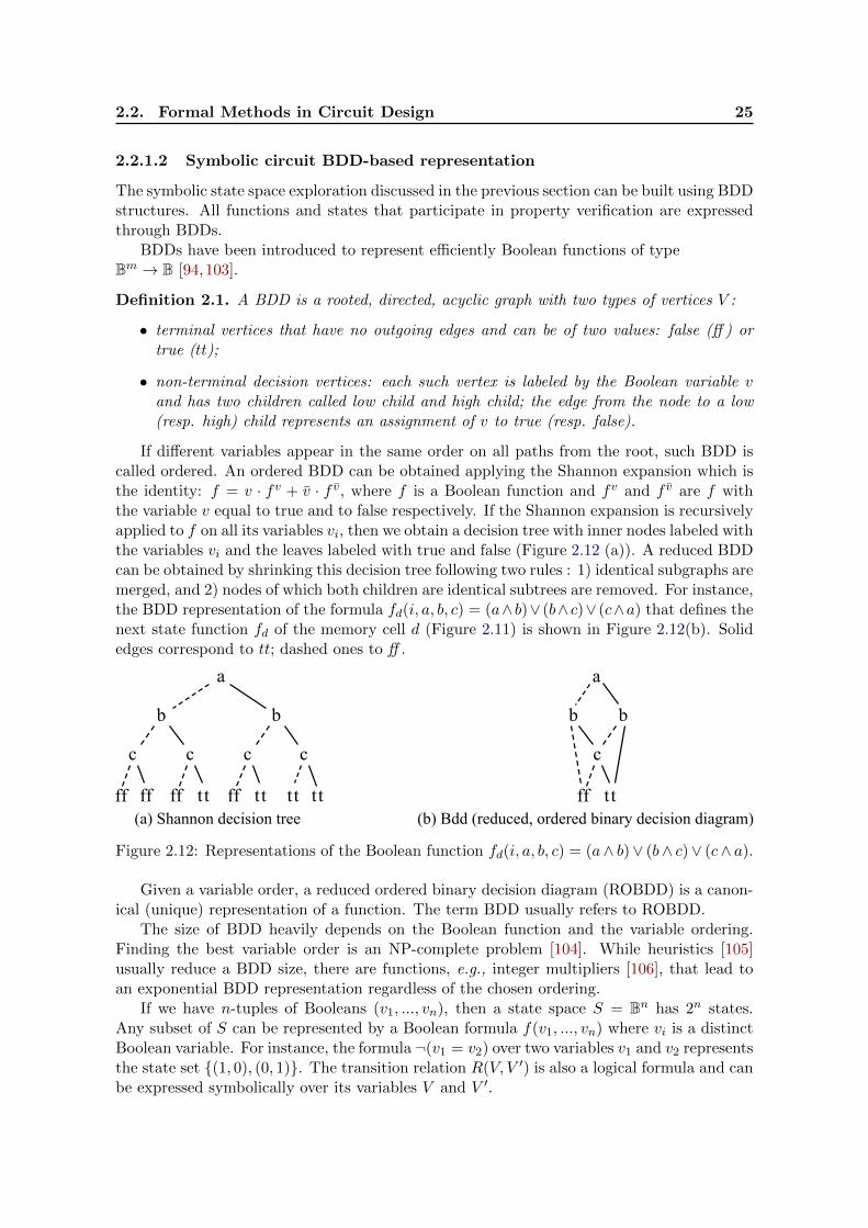
2.2. Formal Methods in Circuit Design 25
2.2.1.2 Symbolic circuit BDD-based representation
The symbolic state space exploration discussed in the previous section can be built using BDDstructures. All functions and states that participate in property verification are expressedthrough BDDs.
BDDs have been introduced to represent efficiently Boolean functions of typeBm → B [94, 103].
Definition 2.1. A BDD is a rooted, directed, acyclic graph with two types of vertices V :
• terminal vertices that have no outgoing edges and can be of two values: false (ff ) ortrue (tt);
• non-terminal decision vertices: each such vertex is labeled by the Boolean variable vand has two children called low child and high child; the edge from the node to a low(resp. high) child represents an assignment of v to true (resp. false).
If different variables appear in the same order on all paths from the root, such BDD iscalled ordered. An ordered BDD can be obtained applying the Shannon expansion which isthe identity: f = v · fv + v · f v, where f is a Boolean function and fv and f v are f withthe variable v equal to true and to false respectively. If the Shannon expansion is recursivelyapplied to f on all its variables vi, then we obtain a decision tree with inner nodes labeled withthe variables vi and the leaves labeled with true and false (Figure 2.12 (a)). A reduced BDDcan be obtained by shrinking this decision tree following two rules : 1) identical subgraphs aremerged, and 2) nodes of which both children are identical subtrees are removed. For instance,the BDD representation of the formula fd(i, a, b, c) = (a∧ b)∨ (b∧ c)∨ (c∧a) that defines thenext state function fd of the memory cell d (Figure 2.11) is shown in Figure 2.12(b). Solidedges correspond to tt; dashed ones to ff .
(a) Shannon decision tree (b) Bdd (reduced, ordered binary decision diagram)
a
b b
c c c c
ff ff ffff tt t t t t t t
a
b b
c
ff tt
Figure 2.12: Representations of the Boolean function fd(i, a, b, c) = (a∧ b)∨ (b∧ c)∨ (c∧ a).
Given a variable order, a reduced ordered binary decision diagram (ROBDD) is a canon-ical (unique) representation of a function. The term BDD usually refers to ROBDD.
The size of BDD heavily depends on the Boolean function and the variable ordering.Finding the best variable order is an NP-complete problem [104]. While heuristics [105]usually reduce a BDD size, there are functions, e.g., integer multipliers [106], that lead toan exponential BDD representation regardless of the chosen ordering.
If we have n-tuples of Booleans (v1, ..., vn), then a state space S = Bn has 2n states.Any subset of S can be represented by a Boolean formula f(v1, ..., vn) where vi is a distinctBoolean variable. For instance, the formula ¬(v1 = v2) over two variables v1 and v2 representsthe state set {(1, 0), (0, 1)}. The transition relation R(V, V ′) is also a logical formula and canbe expressed symbolically over its variables V and V ′.
26 Chapter 2. Circuits Fault-Tolerance and Formal Methods
If the current state set S0 is expressed through the formula f0(~v) (~v = v1, ..., vn) and theformula g(~v, ~v′) represents the transition relation so that {(~v,~v′) | R ~v ~v′}, then the formula∃~v. f0(~v) ∧ g(~v,~v′) represents the reachable state set in one step expressed over variables ~v′:
f1(~v′) = {~v′ | ∃~v. ~v ∈ S0 ∧R ~v ~v′}
Existential quantification ∃ can be computed as the Shannon expansion:
∃vi. f(v1, ..., vi, ...) = f(v1, ..., 1, ...) ∨ f(v1, ..., 0, ...)
Since the next state set f1(~v′) is expressed in terms of variables ~v′ = v′1, ..., v′n, it is needed to
substitute variables ~v′ with old variables ~v to perform the next iteration of reachable stateset calculation. The formula f1[~v′ ← ~v] is identical to f1(~v′) except that each variable v′i ∈ ~v′is replaced with vi ∈ ~v. Consequently, the formula over variables ~v, that represents the stateset S1 reachable in one step, can be expressed as:
f1(~v) = (∃~v. f0(~v) ∧ g(~v,~v′))[~v′ ← ~v]
Thus, the state set Si, reachable in i steps from the original set S0 expressed through thegiven formula f0, can be expressed recursively as:
fi(~v) = (∃~v. fi−1(~v) ∧ g(~v,~v′))[~v′ ← ~v]
For instance, if the initial state of the circuit in Figure 2.11 is {a = 0; b = 0; c = 0; d = 0},it can be expressed as the formula: f0(i, a, b, c, d) = ¬a∧¬b∧¬c∧¬d. The transition relation,derived in Section 2.2.1.1 is:
R(i, a, b, c, d)(i′, a′, b′, c′, d′) = (a′ = i) ∧ (b′ = i) ∧ (c′ = i) ∧ (d′ = (a ∧ b) ∨ (b ∧ c) ∨ (c ∧ a))
Consequently, the next circuit states after its initial one can be expressed by the followingformula:
f1(i, a, b, c, d) = (∃i ∃a ∃b ∃c ∃d. ¬a ∧ ¬b ∧ ¬c ∧ ¬d∧(a′ = i) ∧ (b′ = i) ∧ (c′ = i) ∧ (d′ = (a ∧ b) ∨ (b ∧ c) ∨ (c ∧ a))
)[{i′, a′, b′, c′, d′} ← {i, a, b, c, d}]After the Shannon expansion of the existentials, we get
f1(i, a, b, c, d) = ( ((a′ = 1) ∧ (b′ = 1) ∧ (c′ = 1) ∧ (d′ = 0))∨((a′ = 0) ∧ (b′ = 0) ∧ (c′ = 0) ∧ (d′ = 0))
)[{i′, a′, b′, c′, d′} ← {i, a, b, c, d}]and after variables substitution:
f1(i, a, b, c, d) = ((a = 1) ∧ (b = 1) ∧ (c = 1) ∧ (d = 0))∨((a = 0) ∧ (b = 0) ∧ (c = 0) ∧ (d′ = 0))
Finally, after simplifications: f1(i, a, b, c, d) = ((a ∧ b ∧ c) ∨ (¬a ∧ ¬b ∧ ¬c)) ∧ ¬d.In other words, the next state after the initial one can be either {a = 1; b = 1; c = 1; d = 0}
or {a = 0; b = 0; c = 0; d = 0}. These two scenarios correspond to two input options duringthe first clock cycle: i = 1 and i = 0 respectively. The following state sets fi, i = 2, . . . canbe calculated in a similar manner.
There are three operation types for the discussed symbolic state space exploration: logicaloperations, existential quantification, and variable substitution. All aforementioned opera-tions are provided by the most popular BDD libraries [107, 108] in an efficient manner. InSection 3, we present the symbolic analysis using the BDD library CUDD [107]. The CUDDlibrary implements BDDs based on typed decision graphs [109] that allow reducing the sizeof the used BDD structures by sharing their sub-parts and merging subgraphs.
2.2. Formal Methods in Circuit Design 27
2.2.2 Theorem Proving
Another formal hardware verification approach relies on the description of both the imple-mentation and the specification in a formal logic. The correctness of the implementation isguaranteed by proving in the logic that the implementation corresponds to the specification.Theorem proving is based on formal theories (e.g., propositional calculus, first-order logic,higher-order logic) that define an alphabet, a grammar to construct well-formed formulas,a subset of the formulas, called axioms, and inference rules that can be used to derive newformulas [110].
A formal proof in a formal theory is a finite sequence of well-formed formulas: f1, f2, ..., fn,such that for every i, formula fi either is an axiom or can be derived by one of the inferencerules given the formulas {f1, f2, ..., fi−1} [111]. The last well-formed formula fn is usuallycalled a theorem.
Proofs can be realized with the help of Interactive Theorem Provers (ITPs) (proof assis-tants) where theorems are shown by man-machine interactions. Widely-used ITPs includeACL2 [112], Coq [113], HOL [114], Isabelle [115], Mizar [116], and PVS [117]. An ITP pro-vides its own input language to write proofs, which has features of a programming language,a mathematical typesetting system, and a logic. ITPs can be considered as proof editorswhere a user gives definitions, theorems, and proofs. The theorem correctness should beshown by the user in a formal theory of mathematics. ITPs help the user to prove theo-rems and check the correctness of each proof step. To facilitate and automatize the proofsITPs provide tactics that are able to perform some simple reasoning in an automatic man-ner. The limited automation imposes high manpower and requires an expertise in the usedformal theory. Moreover, a deep understanding of the system implementation, model, andspecification is needed to develop a proper proof strategy that often involves difficult rea-soning. For comparison, model checking does not always require the knowledge of systems’internal properties. The understanding of the overall system behavior is often sufficient.This “black box” and automatic approach does not work in theorem proving. On the otherhand, theorem proving and its richer formalism allow us to express properties that are notin the scope of simpler formalisms or solvable by model checking. For instance, it allowsshowing properties for classes of circuits.
In this dissertation, we use Coq that is based on an expressive formal language calledthe Calculus of Inductive Constructions (CIC) [118,119]. CIC combines a higher-order logicand a richly-typed functional programming language.
In the next section, we provide some intuitions of theorem proving in Coq using simpleexamples. Later, we will show where and how theorem proving has been already used andwhat kind of problems can be solved with this powerful technique.
2.2.2.1 Theorem Proving in Coq by Examples
From now on, text in this style refers to the text that the user sends to Coq, while text inthis style is the answer of the system.
The command Check returns the type of its argument.
Check (3+4).
3+4:nat
The expression (3+4) has type nat, i.e., natural number. The next formula expresses alogical proposition of type Prop:
Check (3≤4).
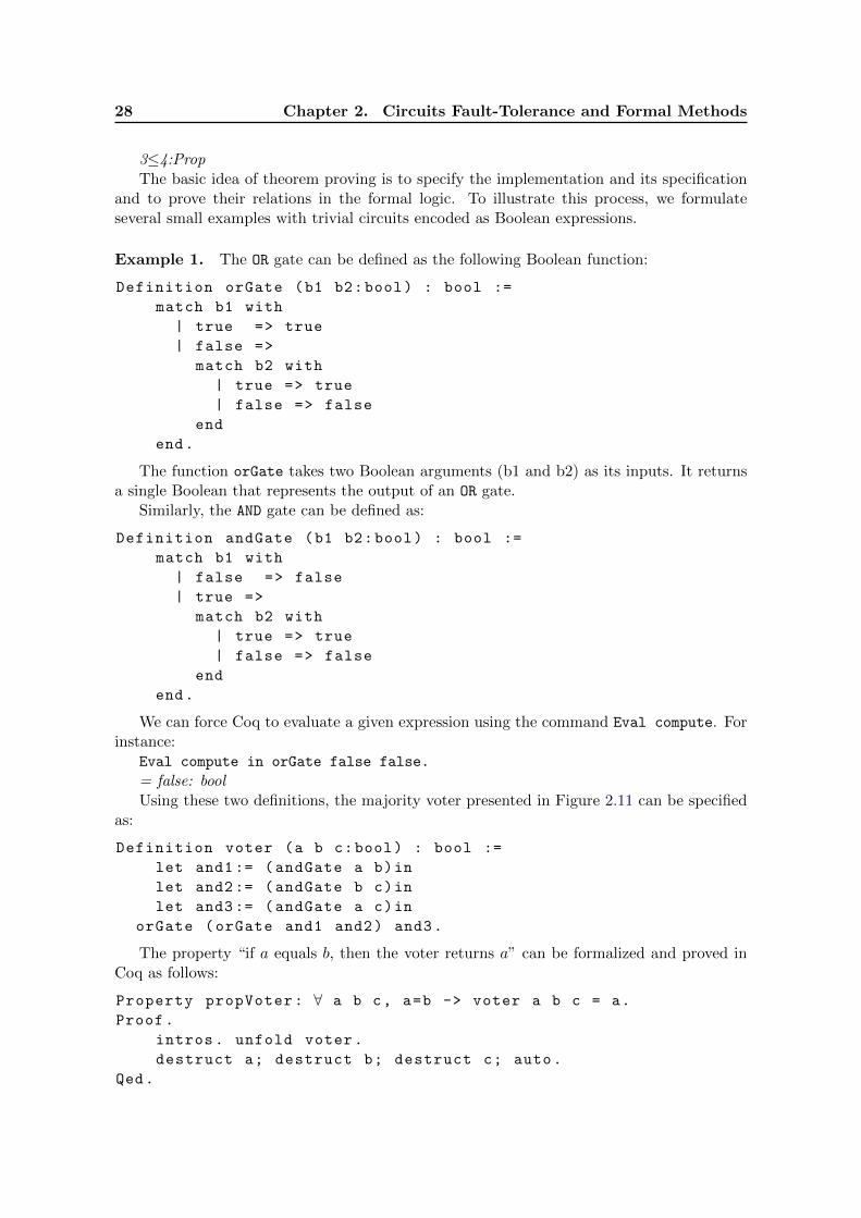
28 Chapter 2. Circuits Fault-Tolerance and Formal Methods
3≤4:PropThe basic idea of theorem proving is to specify the implementation and its specification
and to prove their relations in the formal logic. To illustrate this process, we formulateseveral small examples with trivial circuits encoded as Boolean expressions.
Example 1. The OR gate can be defined as the following Boolean function:
Definition orGate (b1 b2:bool) : bool :=
match b1 with
| true => true
| false =>
match b2 with
| true => true
| false => false
end
end.
The function orGate takes two Boolean arguments (b1 and b2) as its inputs. It returnsa single Boolean that represents the output of an OR gate.
Similarly, the AND gate can be defined as:
Definition andGate (b1 b2:bool) : bool :=
match b1 with
| false => false
| true =>
match b2 with
| true => true
| false => false
end
end.
We can force Coq to evaluate a given expression using the command Eval compute. Forinstance:
Eval compute in orGate false false.
= false: boolUsing these two definitions, the majority voter presented in Figure 2.11 can be specified
as:
Definition voter (a b c:bool) : bool :=
let and1:= (andGate a b)in
let and2:= (andGate b c)in
let and3:= (andGate a c)in
orGate (orGate and1 and2) and3.
The property “if a equals b, then the voter returns a” can be formalized and proved inCoq as follows:
Property propVoter: ∀ a b c, a=b -> voter a b c = a.
Proof.
intros. unfold voter.
destruct a; destruct b; destruct c; auto.
Qed.
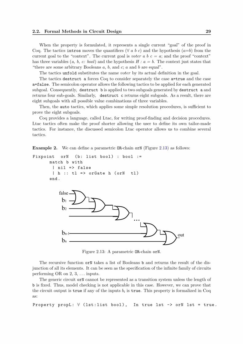
2.2. Formal Methods in Circuit Design 29
When the property is formulated, it represents a single current “goal” of the proof inCoq. The tactics intros moves the quantifiers (∀ a b c) and the hypothesis (a=b) from thecurrent goal to the “context”. The current goal is voter a b c = a; and the proof “context”has three variables (a, b, c: bool) and the hypothesis H : a = b. The context just states that“there are some arbitrary Booleans a, b, and c; a and b are equal”.
The tactics unfold substitutes the name voter by its actual definition in the goal.
The tactics destruct a forces Coq to consider separately the case a=true and the casea=false. The semicolon operator allows the following tactics to be applied for each generatedsubgoal. Consequently, destruct b is applied to two subgoals generated by destruct a andreturns four sub-goals. Similarly, destruct c returns eight subgoals. As a result, there areeight subgoals with all possible value combinations of three variables.
Then, the auto tactics, which applies some simple resolution procedures, is sufficient toprove the eight subgoals.
Coq provides a language, called Ltac, for writing proof-finding and decision procedures.Ltac tactics often make the proof shorter allowing the user to define its own tailor-madetactics. For instance, the discussed semicolon Ltac operator allows us to combine severaltactics.
Example 2. We can define a parametric OR-chain orN (Figure 2.13) as follows:
Fixpoint orN (b: list bool) : bool :=
match b with
| nil => false
| h :: tl => orGate h (orN tl)
end.
false
out
b1
bn
...
bn-1
b2
Figure 2.13: A parametric OR-chain orN.
The recursive function orN takes a list of Booleans b and returns the result of the dis-junction of all its elements. It can be seen as the specification of the infinite family of circuitsperforming OR on 2, 3, . . . inputs.
The generic circuit orN cannot be represented as a transition system unless the length ofb is fixed. Thus, model checking is not applicable in this case. However, we can prove thatthe circuit output is true if any of the inputs bi is true. This property is formalized in Coqas:
Property propL: ∀ (lst:list bool), In true lst -> orN lst = true.
30 Chapter 2. Circuits Fault-Tolerance and Formal Methods
It can be read as: “for all Boolean lists lst, if there is at least one true value in the list,the returned value of orN applied to lst is true”. The proof of the property is given below:
Proof.
intros.
induction lst.
- auto.
- destruct H.
+ rewrite H. auto.
+ apply IHlst in H. simpl. rewrite H. destruct a; auto.
Qed.
The tactics intros moves the quantifiers (∀ lst) and the hypothesis (In true lst) inthe context. The goal becomes: orN lst = true; and the proof “context” has a Booleanlist (lst: list bool) and the hypothesis (H: In true lst).
The most common strategy to prove the property of the inductively defined constructionis the proof by induction. The tactics induction lst realizes an induction on the liststructure and decomposes the current goal into:
• the goal orN [] = true which is easily proven by auto;
• the goal orN (a::lst) = true with the hypotheses : H: In true (a::lst) andIn true lst → orN lst = true
The hypothesis H is destructed in two mutually exclusive cases by destruct H: eithera=true or In true lst. The following proofs for these two cases are split by “+” in thelisting.
For H: a= true, rewrite H substitutes a by true in orN (a::lst) = true and auto
is sufficient to conclude orN (true::lst) = true.
For H: In true lst, we have the induction hypothesis in the context:
IHlst : In true lst -> orN lst = true
Applying IHlst in H, we get H: orN lst = true. Simplification of the goal (simpl)returns orGate a (orN lst) = true; as using H (rewrite H), we get orGate a true =
true. The equation orGate a true = true holds regardless of the value of a. It is shownby destructing a and using auto in each case.
Example 3. In comparison with simple type or set theories used in other ITPs Coq relieson expressive dependent type theory. Dependent types facilitate the encoding of invariants(properties) in the type. We demonstrate this advantage using vectors, a dependent type ofthe standard Coq library. A vector type takes an integer n and returns the type vector ofsize n. That is, the type carries information about the length of the structure. Using thistype, we can define bit vectors as:
Definition Bvector := Vector.t bool.
Bvector takes a nat number n and returns the type vector of bool of size n. It makespossible to verify, for example, the absence of out-of-bounds accesses statically.
Consider the function that represents the family of voters on three buses a, b, and c ofthe same length n:
2.2. Formal Methods in Circuit Design 31
Definition voterBus (n:nat) (a b c: Bvector n): Bvector n:=
let twoF:= Vector.map2 voter a b in
Vector.map2 (fun vi ci => vi ci) twoF c.
We can apply this function to three Boolean vectors of size 2:
voterBus [true;true] [true;false] [false;false]
Its evaluation returns [true; false] of type Bvector 2. Its type explicitly represents thattwo-bit buses are voted and two bits are returned. Dependent types ensure that voterBus
applied to arguments is a well-formed expression. If we used lists, which represent a non-dependent type, only the evaluation of voterBus would return an error if applied to lists ofdifferent lengths.
We use dependent types in Chapter 5 to ensure that circuits are well-formed by construc-tion (gates correctly plugged, no dangling wires, no combinational loops, . . .). For furtherdetails about Coq we refer to the tutorial [120].
Proof by reflection. Proof by reflection [121], available in Coq, allows to replace someproofs by computation. Coq makes a distinction between logical propositions and Booleanvalues. While logical propositions represent objects of type Prop, bool is an inductivedatatype with two constructors true and false. Prop supports natural deduction, whereasstraightforward Boolean function evaluation can be performed in bool. However, Prop andbool are complementary and reflection uses the correspondence between these two domains.Thus, instead of working with a propositional version of decidable predicates, reflection usesthe proof of the needed property on their Boolean equivalents and replaces manual proofsby automatic computation. More precisely, let P : A→ Prop be a predicate of type Propon a type A, let c : A→ bool be a decision procedure on A so that:
Refl : ∀a, c a = true→ P a
We can prove P b by showing that c b = true, which boils down to the evaluation of c b,and by applying Refl. We give more details how reflection is used in this dissertation inSection 5.3.4.
The preceding examples give some intuition how proofs can be performed in Coq andhow circuit properties can be formally proven. In the next section, we consider state-of-artapplications of theorem proving in academy and industry.
2.2.2.2 Theorem Proving Applications
Theorem proving for hardware has been mostly used for functional verification to ensurethe absence of bugs. For instance, as a consequence of the Pentium bug, AMD and Intelincreased their efforts in floating-point verification since the late 1990s [122, 123]. Below wegroup all application cases into three main categories: proof of implementations, proof ofparameterized circuit correctness, and proof of circuit synthesis algorithms.
Implementation correctness
Theorem proving is especially important in safety-critical domains where functional correct-ness prevails the cost of the proof. In [124], Sam Owre, et al. describe the NASA’s experience
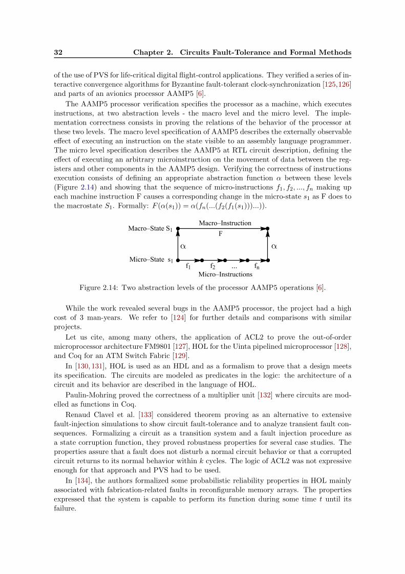
32 Chapter 2. Circuits Fault-Tolerance and Formal Methods
of the use of PVS for life-critical digital flight-control applications. They verified a series of in-teractive convergence algorithms for Byzantine fault-tolerant clock-synchronization [125,126]and parts of an avionics processor AAMP5 [6].
The AAMP5 processor verification specifies the processor as a machine, which executesinstructions, at two abstraction levels - the macro level and the micro level. The imple-mentation correctness consists in proving the relations of the behavior of the processor atthese two levels. The macro level specification of AAMP5 describes the externally observableeffect of executing an instruction on the state visible to an assembly language programmer.The micro level specification describes the AAMP5 at RTL circuit description, defining theeffect of executing an arbitrary microinstruction on the movement of data between the reg-isters and other components in the AAMP5 design. Verifying the correctness of instructionsexecution consists of defining an appropriate abstraction function α between these levels(Figure 2.14) and showing that the sequence of micro-instructions f1, f2, ..., fn making upeach machine instruction F causes a corresponding change in the micro-state s1 as F does tothe macrostate S1. Formally: F (α(s1)) = α(fn(...(f2(f1(s1)))...)).
Micro–Instructions
Macro–Instruction
f2f1 fn...
αMacro–State S1
Micro–State s1
αF
Figure 2.14: Two abstraction levels of the processor AAMP5 operations [6].
While the work revealed several bugs in the AAMP5 processor, the project had a highcost of 3 man-years. We refer to [124] for further details and comparisons with similarprojects.
Let us cite, among many others, the application of ACL2 to prove the out-of-ordermicroprocessor architecture FM9801 [127], HOL for the Uinta pipelined microprocessor [128],and Coq for an ATM Switch Fabric [129].
In [130, 131], HOL is used as an HDL and as a formalism to prove that a design meetsits specification. The circuits are modeled as predicates in the logic: the architecture of acircuit and its behavior are described in the language of HOL.
Paulin-Mohring proved the correctness of a multiplier unit [132] where circuits are mod-elled as functions in Coq.
Renaud Clavel et al. [133] considered theorem proving as an alternative to extensivefault-injection simulations to show circuit fault-tolerance and to analyze transient fault con-sequences. Formalizing a circuit as a transition system and a fault injection procedure asa state corruption function, they proved robustness properties for several case studies. Theproperties assure that a fault does not disturb a normal circuit behavior or that a corruptedcircuit returns to its normal behavior within k cycles. The logic of ACL2 was not expressiveenough for that approach and PVS had to be used.
In [134], the authors formalized some probabilistic reliability properties in HOL mainlyassociated with fabrication-related faults in reconfigurable memory arrays. The propertiesexpressed that the system is capable to perform its function during some time t until itsfailure.
2.2. Formal Methods in Circuit Design 33
Proofs of parameterized circuits
Braibant presented a language-based approach [135] to prove the correctness of parametriccombinational circuits showing the proposed methodology with an example of n-bits adders.The recursive construction scheme of the adder uses a full-adder, i.e., a 1-bit adder, as abasic building block. The presented library features a set of basic blocks and combinatorsthat allows a circuit to be constructed in a hierarchic and modular way as it is done incircuit diagrams. The approach to generate parameterized circuits allows to reason aboutthe parameterized functions rather than about their tangible (fixed-size) instantiations.
A circuit has type C n m, where n and m are types of its inputs and outputs. Since func-tions are used rather than relations, this definition naturally forbids short-circuits, e.g., twoinput ports connected to the same output port. Braibant defines plugs using usual Coqfunctions to get small and computational definitions of maps.
The author shows that dependent types are useful for developing circuits reliably: theresulting circuits are correct by construction (no short circuits, no dangling wires, etc).
Similar work by Qian Wang et al. [136] verifies in Coq a generic logic-level architectureof end-around-carry (EAC) adder, which provides necessary underpinnings for verifying itscustomized and new implementations. In this sense, this works extends [137] where basicadders and their components are verified in Coq. It supplements [137] with arbitrary groupingof arbitrary input data-width, which makes the method more complete. The key elementsof mechanical verification stay the same as in [135]: the data-width is given as a parameter;the correctness of core sub-components are verified separately; and the properties on thegrouping are proven.
Circuit synthesis
ITPs have also been used to certify tools used in circuit synthesis. An old survey of formalcircuit synthesis is given in [138].
More recently, S. Ray et al. proved circuit transformations used in high-level synthesiswith ACL2 [139]. The authors argue that high-level behavioral synthesis has not yet foundwide acceptance in industrial practice because of the lack of confidence in the correctnessof synthesis. The main difficulty is the difference between abstractions used in behavioraldescriptions and in gate-level implementations. They propose to decompose the synthesiscertification into two components for high-level and low-level circuit synthesis, which can berespectively handled by complementary verification techniques: theorem proving and modelchecking.
First, high-level transformations are certified once and for all circuits by theorem proving.These high-level transformations can be grouped into:
1. compiler transformations (e.g., loop unrolling or constant propagation to eliminateunnecessary variables);
2. scheduling (e.g., pipelining);
3. resource binding (e.g., register allocation).
These transformations operate on a graph-based abstraction called clocked control dataflowgraph. After these high-level transformations, proved by construction in ACL2, the designis translated from the control/dataflow graph into RTL circuit description.
34 Chapter 2. Circuits Fault-Tolerance and Formal Methods
The correspondence between the graph-based description and the resulting low-level HDLis verified by model checking techniques. Low-level tweaks and optimizations are handledthrough model checking too. Since the second part is based on model checking, it imposes ascalability bottleneck for the whole technique.
Another work in high-level circuit synthesis is presented by Braibant and Chlipala whocertified in Coq a compiler from a simplified BlueSpec [140] to synthesizable subsets of Verilogand VHDL [141]. Opposed to the previous cases where logical formulas are written directlyin the logic of the theorem prover, the simplified BlueSpec is defined as a dependently typedsyntax in Coq. The defined datatypes represent the syntax of the logic.
Finally, the work [142] defines a compiler of mathematical functions from a synthesizablesubset of HOL to correct-by-construction synchronous circuit in Verilog. This solution forhigh-level synthesis ensures that the resulting gate-level implementation is correct w.r.t. itshigh-level specification.
2.3 Conclusion
We have presented in this chapter background material on circuit fault-tolerance and formalmethods.
While the fault-tolerance domain has existed since the beginning of the computer era, itremains a very conservative area where the techniques developed half of a century ago are stillin use. Even when new challenges appear, such as high electronics sensitivity and increasedtransient fault rates, designers re-use costly but time-proven methods, like TMR. Designersare not keen to combine, optimize, or invent sophisticated fault-tolerance techniques due tothe difficulty to check their correctness and the high cost of possible mistakes. This costis especially obvious in safety-critical applications where a fault-tolerance flaw may lead tothe loss of an aerospace mission or even human lives. Thus, new fault-tolerance solutionseither appear from the academic community [3,66] but are not integrated and used in circuitsynthesis tools or represent specific application-oriented industrial solutions [2, 63,64].
Formal methods in hardware have been used mainly for functional verification. Modelchecking is an automatic method to check if a circuit has desired functional properties.It suffers from a scalability problem, which stays the main research effort in the domain.Theorem proving often requires prohibitive man-power to show the correspondence betweenthe specification and the implementation. However, it is able to assure the correctness ofcircuit families and of synthesis steps for all circuits.
Fault-tolerance domain could benefit from formal methods to guarantee the presence ofrequired properties and to give enough confidence about new techniques and optimizations.This is the aim of the research described in this dissertation. We apply formal methods tooptimize fault-tolerance techniques and to assure their functional and fault-tolerance proper-ties.

Chapter 3
Verification-based VoterMinimization
TMR proposed by von Neumann [54] remains the most popular fault tolerance technique inFPGAs to mask SEUs and SETs. As discussed in Section 2.1.3.1, adding majority votersonly at the primary outputs in a triplicated sequential circuit is not sufficient in general.Voter insertion after each memory cell is sufficient to prevent errors from remaining in cells.However, it increases both hardware overhead and the critical path, which decreases thecircuit maximum frequency.
To the best of our knowledge, there is no tool dedicated to voter minimization in TMRthat guarantees fault-tolerance according to a user-defined fault model. In this section, wepresent a formal solution to minimize the number of voters in TMR sequential circuits,keeping the required fault-tolerance properties. While we focus on voter minimization inTMR circuits, the same approach can be applied to suppress masking mechanisms in time-redundant solutions (see Section 4.2.5).
The chapter starts with the overview of the proposed verification-based approach (Sec-tion 3.1). The first technique step is detailed in Section 3.2 and relies on the circuit syntacticnetlist analysis. The second step is performed by a semantic analysis (Section 3.3) takinginto account the logic of the circuit. When it is known how the circuit is used, we mayuse this input-output specification for further voter number minimization. Section 3.4 andSection 3.5 explain how to benefit from the input and output specifications respectively. InSection 3.6, we extent the fault model from SEUs to SETs. The implementation and exper-iments are presented in Section 3.7. Related works on TMR and voter insertion strategiesare reviewed in Section 3.8. We summarize our contributions in Section 3.9.
3.1 Approach overview
Our objective is to propose an automatic, optimized, and certified transformation processfor TMR on digital circuits. In this chapter, we focus on the optimization aspects of theautomatic transformation: it should insert as few voters as possible, while guaranteeing tomask all errors of the considered fault-model.
We consider first fault models of the form “at most one bit-flip within K cycles”, denotedSEU (1,K). In Section 3.6, we extend our approach to the more general fault-model in theform “at most one transient fault within K clock cycles”, denoted SET (1,K).
The proposed voter-minimization methodology is based on a static analysis that checkswhether an error in a single copy of the TMR circuit may remain after K cycles. If not,protecting the primary outputs with voters is sufficient to mask the error. If, for instance, thecircuit is a pipeline without feedback loops, then any bit-flip will propagate to the outputsand will thus disappear before K cycles, where K is the number of pipeline stages.
But if the state of the circuit is still erroneous after K cycles (in the form of an incorrectvalue stored in one of its memory cells), then there is a potential error accumulation since,
36 Chapter 3. Verification-based Voter Minimization
according to the SEU /SET (1,K) fault models, another fault may occur in another copy ofthe circuit. It may lead to two incorrect redundant modules and errors cannot be masked.In this case, additional voters are needed to prevent error accumulation, that is to mask allerrors circulating inside one redundant module before the next soft-error occurs.
Our static analysis consists of four steps. The first step, described in Section 3.2, ispurely syntactic and finds all loops in the circuit. Error accumulation can be prevented bykeeping enough voters to cut all loops.
In many cases, a digital circuit resets (or overwrites) some memory cells, which may maskerrors. Detecting such cases allows further useless voters to be removed. This second step isperformed by a semantic analysis (Section 3.3) taking into account the logic of the circuit.
Circuits are also often supposed to be used in a specific context. For instance, a circuitspecification may assume that a start signal occurs every x cycles and that outputs areonly read y cycles after each start. When such assumptions exist, taking them into accountmakes the semantic analysis more effective (Sections 3.4 and 3.5).
3.2 Syntactic Analysis
We consider triplicated circuits with voters but we actually work on a single copy of thecircuits. Indeed, the effect of insertion or removal of voters can be represented and analyzedon a single copy of the TMR circuit. We model a sequential circuit C as a directed graph GCwhere each vertex represents a FF (memory cell or latch) and an edge x→ y exists wheneverthere is at least one combinational path between the two FFs x and y in C. An error in acell x may propagate, in the next clock cycle, to all cells connected to x by an edge in thisgraph. Note that this is an over-approximation since the error may actually be masked bysome logical operation.
Under the fault model SEU (1,K), error accumulation is the situation where an errorremains in the circuit K clock cycles after the SEU that caused it. Any circuit C withoutfeedback loop will return, after an SEU, to a correct state before K clock cycles, providedthat K is larger than the maximal length of the paths in GC . Even if our approach can dealwith any K, we can assume that K is a huge number (detailed in Section 2.1.2.1) and islarger than the max length of all paths in GC . It follows that error accumulation can onlybe caused by cycles in GC , which must therefore be cut by removing vertices. Removinga vertex in GC amounts to protecting the corresponding FF with a voter in the triplicatedcircuit.
The best solution to cut all cycles in GC is to find the Minimum Vertex Feedback Set(MVFS), i.e., the smallest set of vertices whose removal leaves GC without cycles. Thisstandard graph problem is NP-hard [143]. While there exist good polynomial time approx-imations [144], the exact algorithm was efficient enough to be used in all our experimentswith relatively small circuits (less than 200 FFs).
Having a voter after each cell belonging to the MVFS prevents error accumulation. Thissimple graph-based analysis is very effective with some classes of circuits. In particular, it issufficient to remove all internal voters in pipelined architectures such as logarithm units andfloating-point multipliers (see Table 3.2.0).
However, this approach is not effective for many circuits due to the extensive use of loopsin circuit synthesis from Mealy machine representation. In such circuits, most memory cellsare in self-loops (e.g., D-type flip-flops with an enable input). This entails many voters if thesyntactic analysis is used alone. However, if the circuit functionality is taken into account,
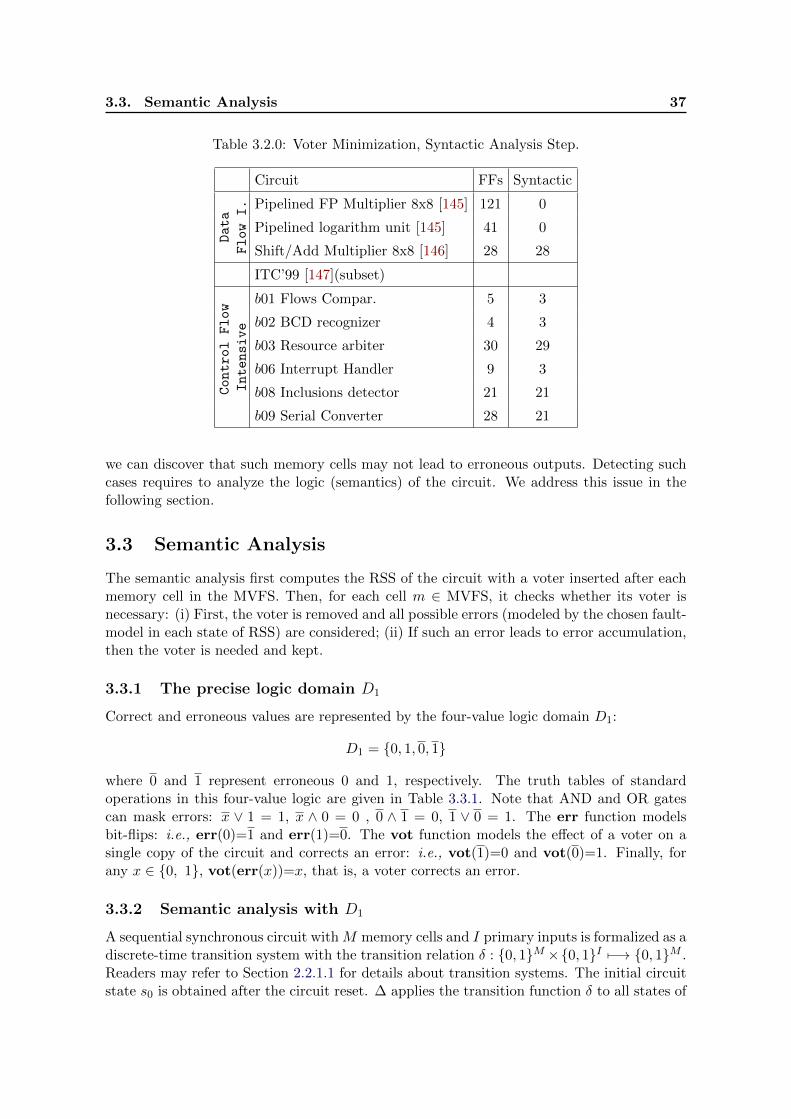
3.3. Semantic Analysis 37
Table 3.2.0: Voter Minimization, Syntactic Analysis Step.
Circuit FFs Syntactic
Data
FlowI. Pipelined FP Multiplier 8x8 [145] 121 0
Pipelined logarithm unit [145] 41 0
Shift/Add Multiplier 8x8 [146] 28 28
ITC’99 [147](subset)
ControlFlow
b01 Flows Compar. 5 3
Intensive b02 BCD recognizer 4 3
b03 Resource arbiter 30 29
b06 Interrupt Handler 9 3
b08 Inclusions detector 21 21
b09 Serial Converter 28 21
we can discover that such memory cells may not lead to erroneous outputs. Detecting suchcases requires to analyze the logic (semantics) of the circuit. We address this issue in thefollowing section.
3.3 Semantic Analysis
The semantic analysis first computes the RSS of the circuit with a voter inserted after eachmemory cell in the MVFS. Then, for each cell m ∈ MVFS, it checks whether its voter isnecessary: (i) First, the voter is removed and all possible errors (modeled by the chosen fault-model in each state of RSS) are considered; (ii) If such an error leads to error accumulation,then the voter is needed and kept.
3.3.1 The precise logic domain D1
Correct and erroneous values are represented by the four-value logic domain D1:
D1 = {0, 1, 0, 1}
where 0 and 1 represent erroneous 0 and 1, respectively. The truth tables of standardoperations in this four-value logic are given in Table 3.3.1. Note that AND and OR gatescan mask errors: x ∨ 1 = 1, x ∧ 0 = 0 , 0 ∧ 1 = 0, 1 ∨ 0 = 1. The err function modelsbit-flips: i.e., err(0)=1 and err(1)=0. The vot function models the effect of a voter on asingle copy of the circuit and corrects an error: i.e., vot(1)=0 and vot(0)=1. Finally, forany x ∈ {0, 1}, vot(err(x))=x, that is, a voter corrects an error.
3.3.2 Semantic analysis with D1
A sequential synchronous circuit with M memory cells and I primary inputs is formalized as adiscrete-time transition system with the transition relation δ : {0, 1}M ×{0, 1}I 7−→ {0, 1}M .Readers may refer to Section 2.2.1.1 for details about transition systems. The initial circuitstate s0 is obtained after the circuit reset. ∆ applies the transition function δ to all states of

38 Chapter 3. Verification-based Voter Minimization
Table 3.3.1: Operators for 4-value logic domain D1
operands 0 10 0 1
1 1 1 1 11 11 1
operands 0 10 0 0 0 01 0 1
0 00 0
NOT err vot0 1 0
1 0
1 1
� �1 0
� 1 1� 0 0
� �
1 0� 1 1� 0 0
10 1
� 0 0 0� 1
its argument set and all possible inputs. Starting from the initial state s0, we compute theset of reachable states RSS by accumulating states obtained by applying iteratively ∆.
The second phase is to check whether the suppression of voters may lead to an erroraccumulation under the chosen fault-model. Let δV be the transition function of a circuitequipped with a voter after each cell in a given set V , and let ∆V be its extension to sets(similarly to the extension of δ into ∆). δV is defined as:
δV ((m1, . . . ,mM ), i) = δ((m′1, . . . ,m′M
), i)
where ∀ 1 ≤ j ≤M, m′j =
{vot(mj) if mj ∈ Vmj otherwise
This checking process is described by Algorithm 1:
Algorithm 1 Semantic Analysis – Main Loop
Input : MVFS ; // The minimum vertex feedback set;∆; // The circuit transition function;s0; // The initial state;
Output : V ; // The subset of vertices (i.e., memorycells) after which a voter is needed
1: V := MVFS ;2: RSS := {s0}∗∆;3: forall m ∈ MVFS4: V := V \{m};5: S := ∆K
V (⋃mi∈M RSS [mi ← err(mi)]);
6: if ErrAcc(S) then7: V := V ∪ {m};8: return V
We start with the circuit equipped with a voter after each cell in the MVFS (line 1). Foreach such cell m, we check whether its voter suppression entails error accumulation. Bit-flips

3.3. Semantic Analysis 39
are introduced in all possible cells and states of RSS according to the fault-model (line 5):⋃mi∈M
RSS [mi ← err(mi)]
The transition function corresponding to the circuit with the current set of voters (V ) isapplied K times (∆K
V ), where K is the number of clock cycles in the fault model (SEU(1,K)).The resulting set of states shows error accumulation if there exists an erroneous cell in atleast one state of this set, which we capture with the predicate ErrAcc in line 6. ErrAcc isdefined as:
ErrAcc(S)⇔ ∃s ∈ S. ∃m ∈ s. m = 0 ∨m = 1
If the set S does not show error accumulation, the voter is useless and can indeed be sup-pressed. Otherwise, the voter is re-introduced (line 7).
In practice, ∆ is applied a small number of times dictated by the circuit functionality andavailable analysis time. It is always safe to stop the iterative computation before reaching K;the only drawback would be to infer an error accumulation when there is none. The numberof ∆ applications can be also adjusted to the available analysis time. In our experiments,the analysis time limit was set to 20 minutes and K to 50. Furthermore, the iteration isstopped:
• if the current set of states is errorless, then there cannot be error accumulation (noerror can reappear);
• or, if the erroneous current set is the same as the previous one, a fixed point is reachedand there is an error accumulation.
The order in which the cells in the MVFS are analyzed (line 2, in Algorithm 1) mayinfluence the number of removed voters. We use the following heuristic to choose the orderingof voter selection: starting from the MVFS of memory cells with voters, we sort it firstaccording to the number of successive memory cells that each cell has in the circuit netlist(the number of successors in GC). Then, we consider primarily the removal of voters thatlead to the corruption of the smallest number of cells in the next clock cycle. The voterswhose removal may lead to a large number of corrupted cells are considered last. We foundout that following this ordering, we are able to suppress more voters than with a randomordering or the ordering relying on the number of preceding memory cells in the netlist.
3.3.3 More Abstract Logic Domains
The aforementioned method is precise but costly since it considers all possible inputs. Ingeneral, keeping track of the relations between indeterminate inputs is not very useful. For-tunately, our technique can be used as is with other, more abstract, logic domains. Thereare several domains that retain enough precision and allow larger circuits to be analyzed.
The 4-value logic domain D2 decreases the state space explosion that occurs with D1:
D2 = {0, 1,U,U}
The abstract value U represents a correct value (either 0 or 1) and U represents any (possiblyerroneous) value (i.e., 0, 1, 0 or 1). A vector of n primary inputs is represented as a uniquevector (U, . . . ,U) with D2 whereas 2n vectors had to be considered with D1. The truthtables of standard operations in D2 are given in Table 3.3.3.
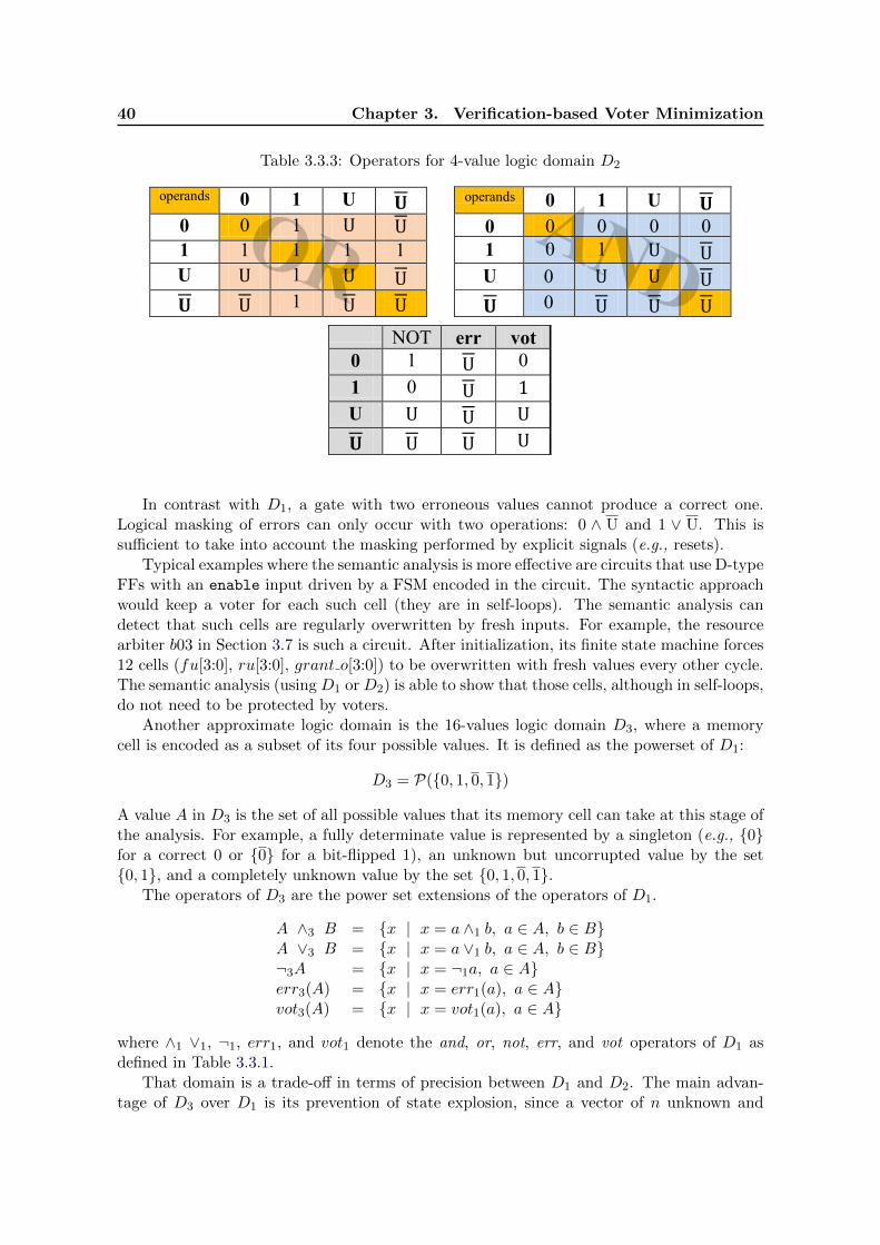
40 Chapter 3. Verification-based Voter Minimization
Table 3.3.3: Operators for 4-value logic domain D2
NOT err vot0 1 U 0
1 0 U 1U U U U
� U U U
0 1 U �0 0 1 U1 1 1 1U U 1 U U� U 1 U U
1U
�operands 0 1 U0 0 0 0 01 0 1 U UU 0 U U� U U0
U
U
In contrast with D1, a gate with two erroneous values cannot produce a correct one.Logical masking of errors can only occur with two operations: 0 ∧ U and 1 ∨ U. This issufficient to take into account the masking performed by explicit signals (e.g., resets).
Typical examples where the semantic analysis is more effective are circuits that use D-typeFFs with an enable input driven by a FSM encoded in the circuit. The syntactic approachwould keep a voter for each such cell (they are in self-loops). The semantic analysis candetect that such cells are regularly overwritten by fresh inputs. For example, the resourcearbiter b03 in Section 3.7 is such a circuit. After initialization, its finite state machine forces12 cells (fu[3:0], ru[3:0], grant o[3:0]) to be overwritten with fresh values every other cycle.The semantic analysis (using D1 or D2) is able to show that those cells, although in self-loops,do not need to be protected by voters.
Another approximate logic domain is the 16-values logic domain D3, where a memorycell is encoded as a subset of its four possible values. It is defined as the powerset of D1:
D3 = P({0, 1, 0, 1})
A value A in D3 is the set of all possible values that its memory cell can take at this stage ofthe analysis. For example, a fully determinate value is represented by a singleton (e.g., {0}for a correct 0 or {0} for a bit-flipped 1), an unknown but uncorrupted value by the set{0, 1}, and a completely unknown value by the set {0, 1, 0, 1}.
The operators of D3 are the power set extensions of the operators of D1.
A ∧3 B = {x | x = a ∧1 b, a ∈ A, b ∈ B}A ∨3 B = {x | x = a ∨1 b, a ∈ A, b ∈ B}¬3A = {x | x = ¬1a, a ∈ A}err3(A) = {x | x = err1(a), a ∈ A}vot3(A) = {x | x = vot1(a), a ∈ A}
where ∧1 ∨1, ¬1, err1, and vot1 denote the and, or, not, err, and vot operators of D1 asdefined in Table 3.3.1.
That domain is a trade-off in terms of precision between D1 and D2. The main advan-tage of D3 over D1 is its prevention of state explosion, since a vector of n unknown and
3.4. Inputs Specification 41
uncorrupted inputs is represented as a unique vector ({0, 1}, . . . , {0, 1}). Contrary to D2, D3
remains able to represent logical masking such as {0} ∧3 {0, 1} = {0} or {1} ∨3 {1, 0} = {1}.Indeed, in D2 we would get U∧2U = U and U∨2U = U . Domain D3 can be seen as retainingprecise information about the possible values and corruptions but ignoring the relationshipsbetween different inputs.
3.4 Inputs Specification
Circuits are often designed to be used in a specific context where some input signals mustoccur at definite timings. Taking into account assumptions about the context may make thesemantic analysis much more precise, in particular, when the logical masking of corruptedcells depends on specific inputs (e.g., a start control signal). Our approach is to translatethese specifications into an interface circuit feeding the original circuit with the specifiedinputs. The analysis of the previous section can then be applied to the resulting combinedcircuit. As a consequence, error accumulation is checked with the method described inSection 3.3.2, but under the constraints specified by the interface. The only small adjustmentneeded in Algorithm 1 is to make sure that errors are introduced only in the cells of theoriginal circuit and not in the cells of the interface circuit.
We use ω-regular expressions to specify circuit interfaces. An ω-regular expression speci-fies constraints using vectors of {0, 1, ?}, which replace primary inputs by 0, 1, or leave themunchanged (? being the wild card). Consider, for instance, a circuit with two primary inputs[i1, i2], then the expression ([1, 0] + [0, 1]).[?, ?]ω specifies that the circuit first reads eitheri1 = 0 and i2 = 1, or i1 = 0 and i2 = 1, and then proceeds with no further constraints.
In general, specifications need non-determinism to describe a partially specified or a non-deterministic context. Hence, the aforementioned ω-regular expression can also be seen as aNon-deterministic Buchi Automaton (NBA) that reads inputs and replaces them by 0, 1, orleaves them unchanged (?).
For instance, the expression ([1, 0]+[0, 1]).[?, ?]ω can be represented as the two-state Non-deterministic Buchi Automaton (NBA) of Figure 3.1 (a): in the first state, it reads inputsand returns either the outputs [1, 0] or [0, 1] (regardless of the inputs). Then, the automatongoes (and stays) in the second state where inputs are read and produced as outputs. Theindices in ?1 and ?2 allow to identify the inputs according to their position.
To generate a circuit from an ω-regular expression, we first convert the correspondingNBA into a deterministic automaton as follows. Each nondeterministic edge is made de-terministic using new inputs (oracles). If a vertex has n nondeterministic outgoing edges,adding log2(n) new inputs is sufficient. For example, the specification ([1, 0] + [0, 1]).[?, ?]ω
can be made deterministic by adding a single additional input i. The automaton (see Fig-ure 3.1 (b)) now reads three inputs: if i is 0 (resp. 1) it produces [1, 0] (resp. [0, 1]). Theresulting deterministic automaton is then translated into an interface circuit using standardlogic synthesis techniques [148, p.118]. If the original circuit has I inputs, the resulting in-terface circuit will have I + a (a oracles to make it deterministic) inputs and I outputs. Itis then plugged by connecting its outputs to the inputs of the circuit to be analyzed.
A typical example where an input specification is useful is the circuit b08 of Section 3.7.Such a circuit has a start input signal and 8-bit data input. Its input interface specificationcan be expressed as the following ω-regular expression:
([1, ?, ?, ?, ?, ?, ?, ?, ?].[0, ?, ?, ?, ?, ?, ?, ?, ?]17)ω (3.1)
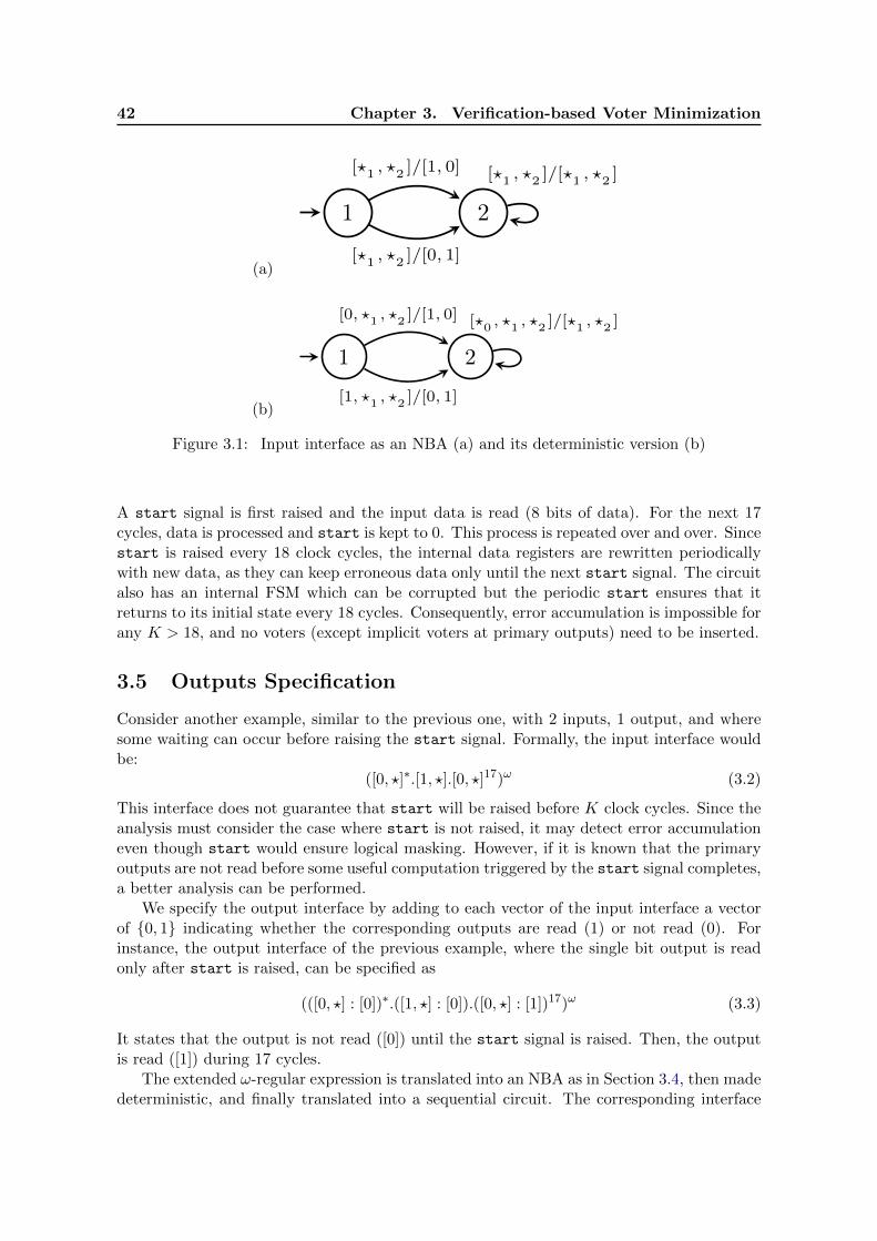
42 Chapter 3. Verification-based Voter Minimization
(a)
1 2
[?1, ?
2]/[1, 0]
[?1, ?
2]/[0, 1]
[?1, ?
2]/[?
1, ?
2]
(b)
1 2
[0, ?1, ?
2]/[1, 0]
[1, ?1, ?
2]/[0, 1]
[?0, ?
1, ?
2]/[?
1, ?
2]
Figure 3.1: Input interface as an NBA (a) and its deterministic version (b)
A start signal is first raised and the input data is read (8 bits of data). For the next 17cycles, data is processed and start is kept to 0. This process is repeated over and over. Sincestart is raised every 18 clock cycles, the internal data registers are rewritten periodicallywith new data, as they can keep erroneous data only until the next start signal. The circuitalso has an internal FSM which can be corrupted but the periodic start ensures that itreturns to its initial state every 18 cycles. Consequently, error accumulation is impossible forany K > 18, and no voters (except implicit voters at primary outputs) need to be inserted.
3.5 Outputs Specification
Consider another example, similar to the previous one, with 2 inputs, 1 output, and wheresome waiting can occur before raising the start signal. Formally, the input interface wouldbe:
([0, ?]∗.[1, ?].[0, ?]17)ω (3.2)
This interface does not guarantee that start will be raised before K clock cycles. Since theanalysis must consider the case where start is not raised, it may detect error accumulationeven though start would ensure logical masking. However, if it is known that the primaryoutputs are not read before some useful computation triggered by the start signal completes,a better analysis can be performed.
We specify the output interface by adding to each vector of the input interface a vectorof {0, 1} indicating whether the corresponding outputs are read (1) or not read (0). Forinstance, the output interface of the previous example, where the single bit output is readonly after start is raised, can be specified as
(([0, ?] : [0])∗.([1, ?] : [0]).([0, ?] : [1])17)ω (3.3)
It states that the output is not read ([0]) until the start signal is raised. Then, the outputis read ([1]) during 17 cycles.
The extended ω-regular expression is translated into an NBA as in Section 3.4, then madedeterministic, and finally translated into a sequential circuit. The corresponding interface
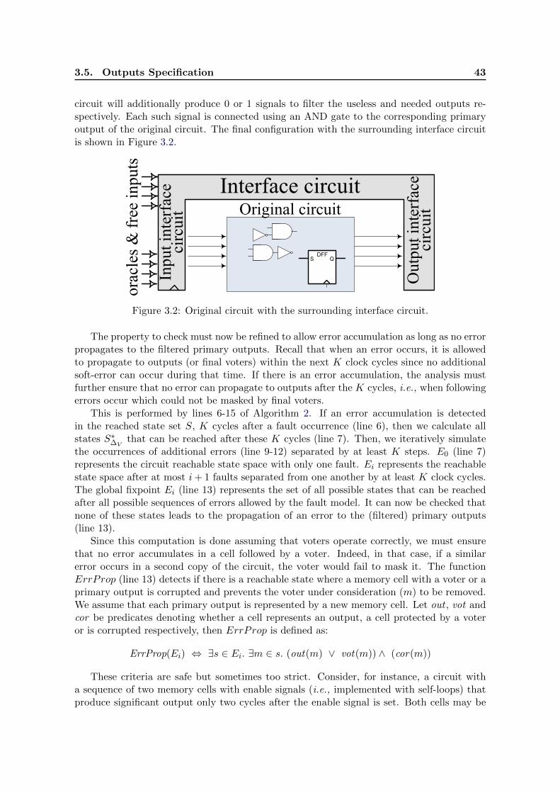
3.5. Outputs Specification 43
circuit will additionally produce 0 or 1 signals to filter the useless and needed outputs re-spectively. Each such signal is connected using an AND gate to the corresponding primaryoutput of the original circuit. The final configuration with the surrounding interface circuitis shown in Figure 3.2.
Inpu
t int
erfa
ceci
rcui
t
orac
les
&fr
ee in
puts
Interface circuit
Out
put i
nter
face
circ
uitOriginal circuit
Figure 3.2: Original circuit with the surrounding interface circuit.
The property to check must now be refined to allow error accumulation as long as no errorpropagates to the filtered primary outputs. Recall that when an error occurs, it is allowedto propagate to outputs (or final voters) within the next K clock cycles since no additionalsoft-error can occur during that time. If there is an error accumulation, the analysis mustfurther ensure that no error can propagate to outputs after the K cycles, i.e., when followingerrors occur which could not be masked by final voters.
This is performed by lines 6-15 of Algorithm 2. If an error accumulation is detectedin the reached state set S, K cycles after a fault occurrence (line 6), then we calculate allstates S∗∆V
that can be reached after these K cycles (line 7). Then, we iteratively simulatethe occurrences of additional errors (line 9-12) separated by at least K steps. E0 (line 7)represents the circuit reachable state space with only one fault. Ei represents the reachablestate space after at most i+ 1 faults separated from one another by at least K clock cycles.The global fixpoint Ei (line 13) represents the set of all possible states that can be reachedafter all possible sequences of errors allowed by the fault model. It can now be checked thatnone of these states leads to the propagation of an error to the (filtered) primary outputs(line 13).
Since this computation is done assuming that voters operate correctly, we must ensurethat no error accumulates in a cell followed by a voter. Indeed, in that case, if a similarerror occurs in a second copy of the circuit, the voter would fail to mask it. The functionErrProp (line 13) detects if there is a reachable state where a memory cell with a voter or aprimary output is corrupted and prevents the voter under consideration (m) to be removed.We assume that each primary output is represented by a new memory cell. Let out , vot andcor be predicates denoting whether a cell represents an output, a cell protected by a voteror is corrupted respectively, then ErrProp is defined as:
ErrProp(Ei) ⇔ ∃s ∈ Ei. ∃m ∈ s. (out(m) ∨ vot(m)) ∧ (cor(m))
These criteria are safe but sometimes too strict. Consider, for instance, a circuit witha sequence of two memory cells with enable signals (i.e., implemented with self-loops) thatproduce significant output only two cycles after the enable signal is set. Both cells may be
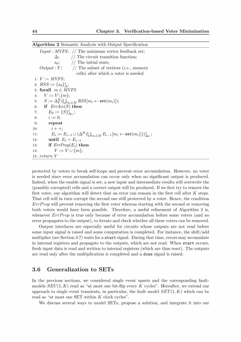
44 Chapter 3. Verification-based Voter Minimization
Algorithm 2 Semantic Analysis with Output Specification
Input : MVFS ; // The minimum vertex feedback set;∆; // The circuit transition function;s0; // The initial state;
Output : V ; // The subset of vertices (i.e., memorycells) after which a voter is needed
1: V := MVFS ;2: RSS := {s0}∗∆;3: forall m ∈ MVFS4: V := V \{m};5: S := ∆K
V (⋃mi∈M RSS [mi ← err(mi)]);
6: if ErrAcc(S) then7: E0 := {S}∗∆V
;8: i := 0;9: repeat
10: i+ +;11: Ei := Ei−1 ∪ (∆K(
⋃mi∈M Ei−1 [mi ← err(mi)]))
∗∆V
;12: until Ei = Ei−1
13: if ErrProp(Ei) then14: V := V ∪ {m};15: return V
protected by voters to break self-loops and prevent error accumulation. However, no voteris needed since error accumulation can occur only when no significant output is produced.Indeed, when the enable signal is set, a new input and intermediate results will overwrite the(possibly corrupted) cells and a correct output will be produced. If we first try to remove thefirst voter, our algorithm will detect that an error can remain in the first cell after K steps.That cell will in turn corrupt the second one still protected by a voter. Hence, the conditionErrProp will prevent removing the first voter whereas starting with the second or removingboth voters would have been possible. Therefore, a useful refinement of Algorithm 2 is,whenever ErrProp is true only because of error accumulation before some voters (and noerror propagates to the output), to iterate and check whether all these voters can be removed.
Output interfaces are especially useful for circuits whose outputs are not read beforesome input signal is raised and some computation is completed. For instance, the shift/addmultiplier (see Section 3.7) waits for a start signal. During that time, errors may accumulatein internal registers and propagate to the outputs, which are not read. When start occurs,fresh input data is read and written to internal registers (which are thus reset). The outputsare read only after the multiplication is completed and a done signal is raised.
3.6 Generalization to SETs
In the previous sections, we considered single event upsets and the corresponding fault-models SEU(1,K) read as “at most one bit-flip every K cycles”. Hereafter, we extend ourapproach to single event transients, in particular, the fault model SET (1,K) which can beread as “at most one SET within K clock cycles”.
We discuss several ways to model SETs, propose a solution, and integrate it into our

3.6. Generalization to SETs 45
previous analysis.
3.6.1 Precise modeling of SETs
As opposed to an SEU, the effect of an SET depends on the logical propagation (and possiblelogical masking) of the signal perturbation through the combinational part. Such signalperturbation or a glitch is latched in a non-deterministic manner. From now on, a signal cantake 3 values: a logical one, a logical zero, or a glitch written �.
Signal := 0 | 1 | �
A glitch can be masked in a combinatorial circuit by or(�, 1) = 1 or and(�, 0) = 0.The precise modelling of a glitched signal in a TMR circuit requires the knowledge of itscorrect value (present in the corresponding signals of the two other redundant modules).Consequently, the precise domain D1 is extended as Dt to model a glitch propagation in acombinatorial circuit of one redundant module:
Dt = {0, 1, 0, 1, 0�, 1�}
where 0� and 1� represent respectively a glitched 0 and 1. That is, 0� represents a glitch atone point of the circuit such that the value in the two other redundant copies is 0. A glitchon an incorrect signal with the value 0 (resp. 1) will be represented by the signal value 1�
(resp. 0�). The following example illustrates the difference between a glitch and a corruptedvalue:
D1 : 0 ∨1 1 = 1 Dt : 0� ∨t 1� = 1�
While in the first case, an or gate with corrupted but stable signals returns a correctvalue, in the second case, the glitch propagates.
While the precise domain D1 requires the aforementioned extension to Dt, the domainsD2 and D3 can overapproximate such glitch behavior with no extension. In particular, aglitched signal, as well as any possibly wrong stable signal, takes the value U in D2. Aglitched 1 (resp. 0) can be represented as {1, 0} (resp. {0, 1}) in D3.
A glitch propagated to a memory cell is non-deterministically latched as true or false.It follows that the precise glitch modelling in Dt implies that any glitched signal 0� (resp.1�) is non-deterministically latched as a correct 0 or as an incorrect 1 (resp. as a correct 1or as an incorrect 0). This non-determinism may lead to a significant state space growth inD1. The domains D2 and D3 avoid this drawback since glitched signals are expressed in thesame logic as the latched values.
To take into consideration all possible effects of an SET, it is necessary to calculate theset of reachable states for all cases of SET injections. These cases include a fault injectionat the output of a logical gate or a memory cell. The union of the state spaces that can bereached in each of these corruption cases forms the reachable state set.
The precise SET modeling in Dt imposes significant computational overhead. Its twoimportant bottlenecks are the need to consider all possible SET injection points and allpossible non-deterministic choices when a glitch is latched. Both points can been taken intoaccount by a transition function that expresses a circuit state change during a clock cyclewith an SET and returns a set of possibly corrupted states. In the next Section, we proposea safe approximation of the precise SET modeling in domains D1, D2, and D3.
46 Chapter 3. Verification-based Voter Minimization
3.6.2 Safe SET over-approximation
If a memory cell is connected by a combinational path to a component (wire or gate) wherean SET occurs, this cell may be corrupted. We should find all sets of cells that can becorrupted at the same clock cycle to find the worst case. Each of these sets has a commoncombinational sub-circuit, in other words, a common “combinational cone”. The apex ofsuch a cone is either the output of a memory cell or a primary input. A cone apex fullyidentifies a cone and the memory cells belonging to this cone.
D Q
D Q
primary input
D Q
logic
logic
logic
c1
f1
f2
f3
c2
c3
p1
Figure 3.3: Combinational cones for SET modeling.
In Figure 3.3, the cone with apex at c1 includes both cells c2 and c3. The cone withapex at p1 also includes {c1, c2}. The cones with apexes at c3 and c2 contain {c1} and {c2}respectively.
As a result, the worst-case scenario of any SET that happens inside a cone j is the unionof all possible simultaneous corruptions of the memory cells ms(j) in this cone. The powerset P (ms(j)) is the set of all possible memory cell corruption configurations.
As soon as all corruption configurations are found, a new error injection procedure canbe defined and used in both Algorithms 1 and 2. In particular, instead of mutually exclusivebit-flips injection to a state space S, expressed for SEU as (
⋃mi∈M S [mi ← err(mi)]), the
corruption of the RSS by an SET is computed as the disjunction of possible simultaneousmemory cells corruptions of the sets included in the cones after memory cells M or primaryinputs I:
⋃j∈(M∪I)
⋃p∈P (ms(j))
S
[ ⋂mi∈p
mi ← err(mi)
]where ms(j) is the subset of memory cells located in the cone with an apex at a memory
cell or a primary input j.
Such corruption procedure is a safe over-approximation in the precise (Dt) and approx-imate (D2, D3) domains. The complexity bottleneck of the approach is the power-set com-putation with a large number of memory cells in a single cone. However, in the case of theapproximate logic domains D2 and D3, we can consider only the worst-case scenario: thesimultaneous corruption of all memory cells in a cone (without calculation of its powerset),
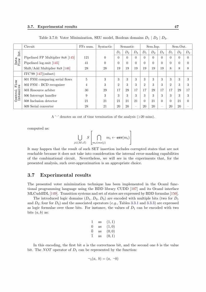
3.7. Experimental results 47
Table 3.7.0: Voter Minimization, SEU model, Boolean domains D1 | D2 | D3.
Circuit FFs num. Syntactic Semantic Sem.Inp. Sem.Out.
Data
FlowInt.
D1 D2 D3 D1 D2 D3 D1 D2 D3
Pipelined FP Multiplier 8x8 [145] 121 0 0 0 0 0 0 0 0 0 0
Pipelined log.unit [145] 41 0 0 0 0 0 0 0 0 0 0
Shift/Add Multiplier 8x8 [146] 28 28 19 19 19 19 19 19 8 8 8
ITC’99 [147](subset)
ControlFlow b01 FSM comparing serial flows 5 3 3 3 3 3 3 3 3 3 3
Intensive b02 FSM - BCD recognizer 4 3 2 3 3 2 3 3 2 3 3
b03 Resource arbiter 30 29 17 29 17 17 29 17 17 29 17
b06 Interrupt handler 9 3 3 3 3 3 3 3 3 3 3
b08 Inclusion detector 21 21 21 21 21 0 21 0 0 21 0
b09 Serial converter 28 21 20 20 – 20 20 – 20 20 –
A ’–’ denotes an out of time termination of the analysis (>20 mins).
computed as: ⋃j∈(M∪I)
S
⋂mi∈ms(j)
mi ← err(mi)
It may happen that the result of such SET insertion includes corrupted states that are notreachable because it does not take into consideration the internal error-masking capabilitiesof the combinational circuit. Nevertheless, we will see in the experiments that, for thepresented analysis, such over-approximation is an appropriate choice.
3.7 Experimental results
The presented voter minimization technique has been implemented in the Ocaml func-tional programming language using the BDD library CUDD [107] and its Ocaml interfaceMLCuddIDL [149]. Transition systems and set of states are expressed by BDD formulas [150].
The introduced logic domains (D1, D2, D3) are encoded with multiple bits (two for D1
and D2; four for D3) and the associated operators (e.g., Tables 3.3.1 and 3.3.3) are expressedas logic formulae over those bits. For instance, the values of D1 can be encoded with twobits (a, b) as:
1 as (1, 1)0 as (1, 0)0 as (0, 0)1 as (0, 1)
In this encoding, the first bit a is the correctness bit, and the second one b is the valuebit. The NOT operator of D1 can be represented by the function:
¬1(a, b) = (a, ¬b)
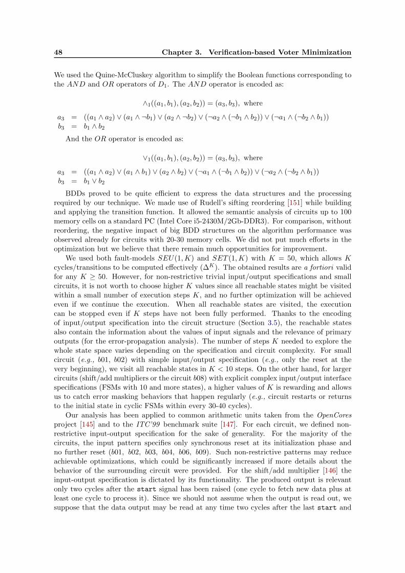
48 Chapter 3. Verification-based Voter Minimization
We used the Quine-McCluskey algorithm to simplify the Boolean functions corresponding tothe AND and OR operators of D1. The AND operator is encoded as:
∧1((a1, b1), (a2, b2)) = (a3, b3), where
a3 = ((a1 ∧ a2) ∨ (a1 ∧ ¬b1) ∨ (a2 ∧ ¬b2) ∨ (¬a2 ∧ (¬b1 ∧ b2)) ∨ (¬a1 ∧ (¬b2 ∧ b1))b3 = b1 ∧ b2
And the OR operator is encoded as:
∨1((a1, b1), (a2, b2)) = (a3, b3), where
a3 = ((a1 ∧ a2) ∨ (a1 ∧ b1) ∨ (a2 ∧ b2) ∨ (¬a1 ∧ (¬b1 ∧ b2)) ∨ (¬a2 ∧ (¬b2 ∧ b1))b3 = b1 ∨ b2
BDDs proved to be quite efficient to express the data structures and the processingrequired by our technique. We made use of Rudell’s sifting reordering [151] while buildingand applying the transition function. It allowed the semantic analysis of circuits up to 100memory cells on a standard PC (Intel Core i5-2430M/2Gb-DDR3). For comparison, withoutreordering, the negative impact of big BDD structures on the algorithm performance wasobserved already for circuits with 20-30 memory cells. We did not put much efforts in theoptimization but we believe that there remain much opportunities for improvement.
We used both fault-models SEU(1,K) and SET (1,K) with K = 50, which allows Kcycles/transitions to be computed effectively (∆K). The obtained results are a fortiori validfor any K ≥ 50. However, for non-restrictive trivial input/output specifications and smallcircuits, it is not worth to choose higher K values since all reachable states might be visitedwithin a small number of execution steps K, and no further optimization will be achievedeven if we continue the execution. When all reachable states are visited, the executioncan be stopped even if K steps have not been fully performed. Thanks to the encodingof input/output specification into the circuit structure (Section 3.5), the reachable statesalso contain the information about the values of input signals and the relevance of primaryoutputs (for the error-propagation analysis). The number of steps K needed to explore thewhole state space varies depending on the specification and circuit complexity. For smallcircuit (e.g., b01, b02) with simple input/output specification (e.g., only the reset at thevery beginning), we visit all reachable states in K < 10 steps. On the other hand, for largercircuits (shift/add multipliers or the circuit b08) with explicit complex input/output interfacespecifications (FSMs with 10 and more states), a higher values of K is rewarding and allowsus to catch error masking behaviors that happen regularly (e.g., circuit restarts or returnsto the initial state in cyclic FSMs within every 30-40 cycles).
Our analysis has been applied to common arithmetic units taken from the OpenCoresproject [145] and to the ITC’99 benchmark suite [147]. For each circuit, we defined non-restrictive input-output specification for the sake of generality. For the majority of thecircuits, the input pattern specifies only synchronous reset at its initialization phase andno further reset (b01, b02, b03, b04, b06, b09). Such non-restrictive patterns may reduceachievable optimizations, which could be significantly increased if more details about thebehavior of the surrounding circuit were provided. For the shift/add multiplier [146] theinput-output specification is dictated by its functionality. The produced output is relevantonly two cycles after the start signal has been raised (one cycle to fetch new data plus atleast one cycle to process it). Since we should not assume when the output is read out, wesuppose that the data output may be read at any time two cycles after the last start and
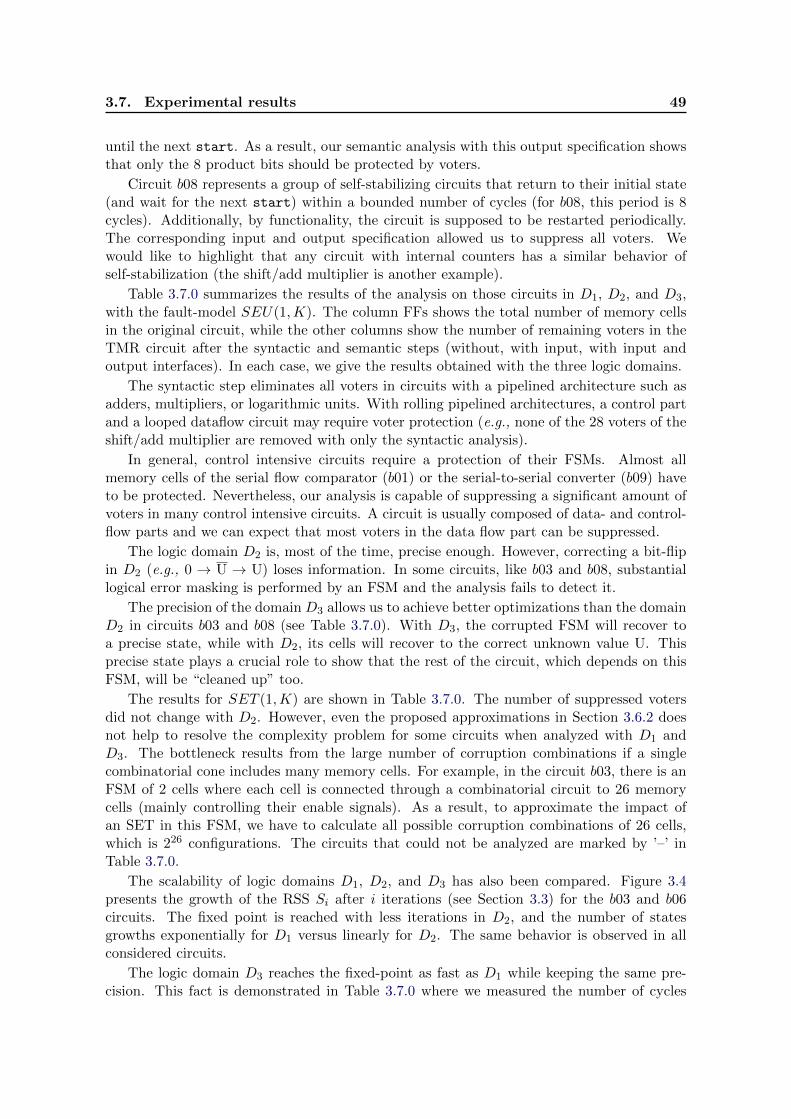
3.7. Experimental results 49
until the next start. As a result, our semantic analysis with this output specification showsthat only the 8 product bits should be protected by voters.
Circuit b08 represents a group of self-stabilizing circuits that return to their initial state(and wait for the next start) within a bounded number of cycles (for b08, this period is 8cycles). Additionally, by functionality, the circuit is supposed to be restarted periodically.The corresponding input and output specification allowed us to suppress all voters. Wewould like to highlight that any circuit with internal counters has a similar behavior ofself-stabilization (the shift/add multiplier is another example).
Table 3.7.0 summarizes the results of the analysis on those circuits in D1, D2, and D3,with the fault-model SEU(1,K). The column FFs shows the total number of memory cellsin the original circuit, while the other columns show the number of remaining voters in theTMR circuit after the syntactic and semantic steps (without, with input, with input andoutput interfaces). In each case, we give the results obtained with the three logic domains.
The syntactic step eliminates all voters in circuits with a pipelined architecture such asadders, multipliers, or logarithmic units. With rolling pipelined architectures, a control partand a looped dataflow circuit may require voter protection (e.g., none of the 28 voters of theshift/add multiplier are removed with only the syntactic analysis).
In general, control intensive circuits require a protection of their FSMs. Almost allmemory cells of the serial flow comparator (b01) or the serial-to-serial converter (b09) haveto be protected. Nevertheless, our analysis is capable of suppressing a significant amount ofvoters in many control intensive circuits. A circuit is usually composed of data- and control-flow parts and we can expect that most voters in the data flow part can be suppressed.
The logic domain D2 is, most of the time, precise enough. However, correcting a bit-flipin D2 (e.g., 0 → U → U) loses information. In some circuits, like b03 and b08, substantiallogical error masking is performed by an FSM and the analysis fails to detect it.
The precision of the domain D3 allows us to achieve better optimizations than the domainD2 in circuits b03 and b08 (see Table 3.7.0). With D3, the corrupted FSM will recover toa precise state, while with D2, its cells will recover to the correct unknown value U. Thisprecise state plays a crucial role to show that the rest of the circuit, which depends on thisFSM, will be “cleaned up” too.
The results for SET (1,K) are shown in Table 3.7.0. The number of suppressed votersdid not change with D2. However, even the proposed approximations in Section 3.6.2 doesnot help to resolve the complexity problem for some circuits when analyzed with D1 andD3. The bottleneck results from the large number of corruption combinations if a singlecombinatorial cone includes many memory cells. For example, in the circuit b03, there is anFSM of 2 cells where each cell is connected through a combinatorial circuit to 26 memorycells (mainly controlling their enable signals). As a result, to approximate the impact ofan SET in this FSM, we have to calculate all possible corruption combinations of 26 cells,which is 226 configurations. The circuits that could not be analyzed are marked by ’–’ inTable 3.7.0.
The scalability of logic domains D1, D2, and D3 has also been compared. Figure 3.4presents the growth of the RSS Si after i iterations (see Section 3.3) for the b03 and b06circuits. The fixed point is reached with less iterations in D2, and the number of statesgrowths exponentially for D1 versus linearly for D2. The same behavior is observed in allconsidered circuits.
The logic domain D3 reaches the fixed-point as fast as D1 while keeping the same pre-cision. This fact is demonstrated in Table 3.7.0 where we measured the number of cycles
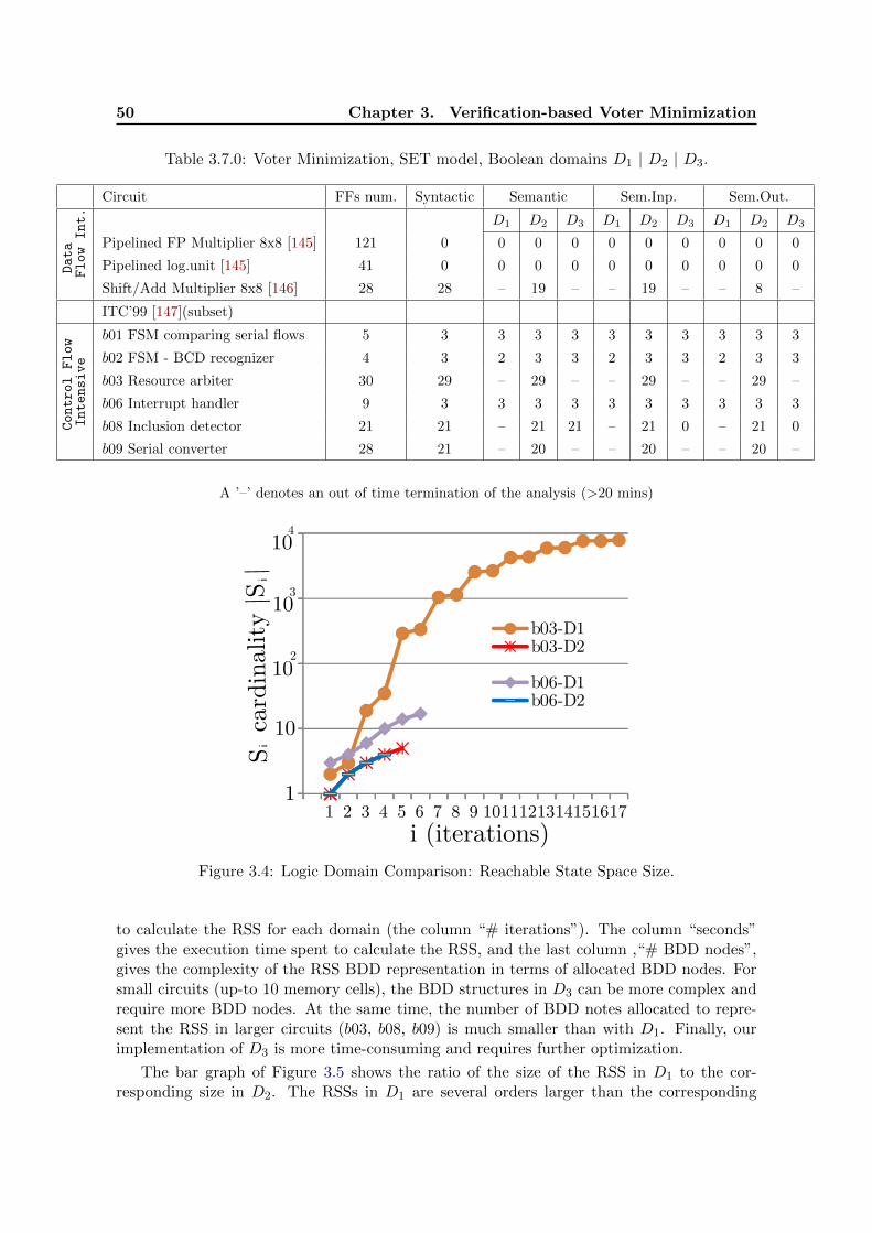
50 Chapter 3. Verification-based Voter Minimization
Table 3.7.0: Voter Minimization, SET model, Boolean domains D1 | D2 | D3.
Circuit FFs num. Syntactic Semantic Sem.Inp. Sem.Out.
Data
FlowInt.
D1 D2 D3 D1 D2 D3 D1 D2 D3
Pipelined FP Multiplier 8x8 [145] 121 0 0 0 0 0 0 0 0 0 0
Pipelined log.unit [145] 41 0 0 0 0 0 0 0 0 0 0
Shift/Add Multiplier 8x8 [146] 28 28 – 19 – – 19 – – 8 –
ITC’99 [147](subset)
ControlFlow b01 FSM comparing serial flows 5 3 3 3 3 3 3 3 3 3 3
Intensive b02 FSM - BCD recognizer 4 3 2 3 3 2 3 3 2 3 3
b03 Resource arbiter 30 29 – 29 – – 29 – – 29 –
b06 Interrupt handler 9 3 3 3 3 3 3 3 3 3 3
b08 Inclusion detector 21 21 – 21 21 – 21 0 – 21 0
b09 Serial converter 28 21 – 20 – – 20 – – 20 –
A ’–’ denotes an out of time termination of the analysis (>20 mins)
1 2 3 4 5 6 7 8 9 1011121314151617
b03-D2b03-D1
b06-D2b06-D1
101
102
103104
S cardi
nality |S
| i
i
b03-D2b03-D1
b06-D2b06-D1
b03-D2b03-D1
b06-D2b06-D1
i (iterations)Figure 3.4: Logic Domain Comparison: Reachable State Space Size.
to calculate the RSS for each domain (the column “# iterations”). The column “seconds”gives the execution time spent to calculate the RSS, and the last column ,“# BDD nodes”,gives the complexity of the RSS BDD representation in terms of allocated BDD nodes. Forsmall circuits (up-to 10 memory cells), the BDD structures in D3 can be more complex andrequire more BDD nodes. At the same time, the number of BDD notes allocated to repre-sent the RSS in larger circuits (b03, b08, b09) is much smaller than with D1. Finally, ourimplementation of D3 is more time-consuming and requires further optimization.
The bar graph of Figure 3.5 shows the ratio of the size of the RSS in D1 to the cor-responding size in D2. The RSSs in D1 are several orders larger than the corresponding
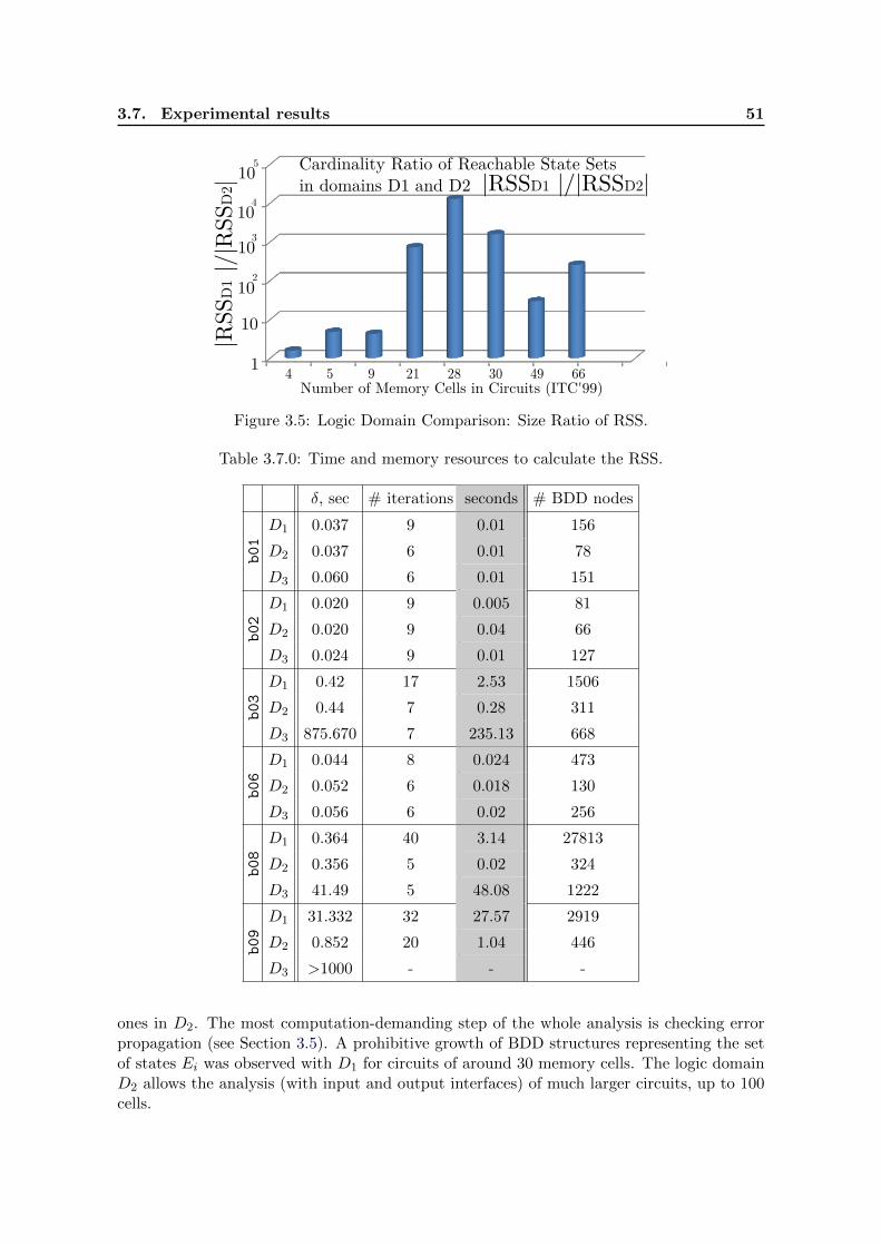
3.7. Experimental results 51
4 5 9 21 28 30 49 66
Cardinality Ratio of Reachable State Setsin domains D1 and D2
Number)of)Memory)Cells)in)Circuits)/ITC|99)1
10102103104105
|RRSD1 |/|RRSD2|Cardinality Ratio of Reachable State Setsin domains D1 and D2 |RRSD1 |/|RRSD2|Cardinality)Ratio)of)Reachable)State)Setsin)domains)D1)and)D2) |RSSD1)|/|RSSD2|
|RSSD1)
|/|RSSD
2|
Figure 3.5: Logic Domain Comparison: Size Ratio of RSS.
Table 3.7.0: Time and memory resources to calculate the RSS.
δ, sec # iterations seconds # BDD nodes
b01
D1 0.037 9 0.01 156
D2 0.037 6 0.01 78
D3 0.060 6 0.01 151
b02
D1 0.020 9 0.005 81
D2 0.020 9 0.04 66
D3 0.024 9 0.01 127
b03
D1 0.42 17 2.53 1506
D2 0.44 7 0.28 311
D3 875.670 7 235.13 668
b06
D1 0.044 8 0.024 473
D2 0.052 6 0.018 130
D3 0.056 6 0.02 256
b08
D1 0.364 40 3.14 27813
D2 0.356 5 0.02 324
D3 41.49 5 48.08 1222
b09
D1 31.332 32 27.57 2919
D2 0.852 20 1.04 446
D3 >1000 - - -
ones in D2. The most computation-demanding step of the whole analysis is checking errorpropagation (see Section 3.5). A prohibitive growth of BDD structures representing the setof states Ei was observed with D1 for circuits of around 30 memory cells. The logic domainD2 allows the analysis (with input and output interfaces) of much larger circuits, up to 100cells.
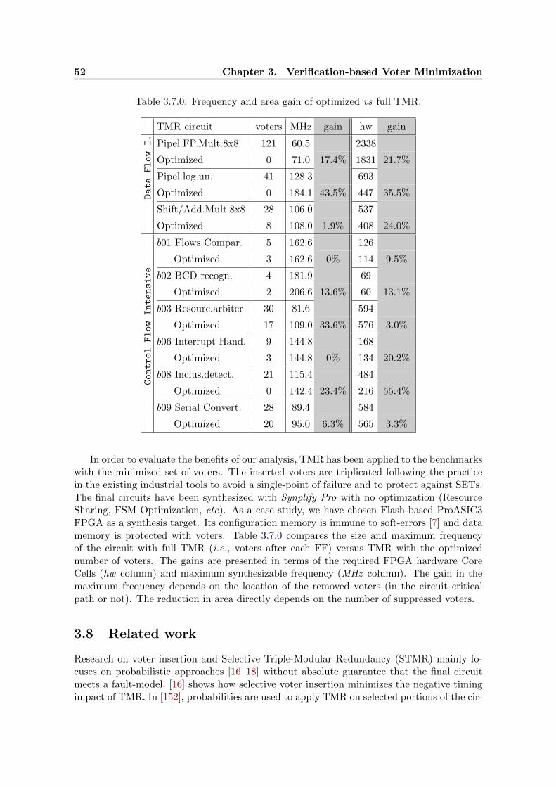
52 Chapter 3. Verification-based Voter Minimization
Table 3.7.0: Frequency and area gain of optimized vs full TMR.
TMR circuit voters MHz gain hw gain
DataFlowI.
Pipel.FP.Mult.8x8 121 60.5 2338
Optimized 0 71.0 17.4% 1831 21.7%
Pipel.log.un. 41 128.3 693
Optimized 0 184.1 43.5% 447 35.5%
Shift/Add.Mult.8x8 28 106.0 537
Optimized 8 108.0 1.9% 408 24.0%
b01 Flows Compar. 5 162.6 126
Optimized 3 162.6 0% 114 9.5%
ControlFlowIntensive
b02 BCD recogn. 4 181.9 69
Optimized 2 206.6 13.6% 60 13.1%
b03 Resourc.arbiter 30 81.6 594
Optimized 17 109.0 33.6% 576 3.0%
b06 Interrupt Hand. 9 144.8 168
Optimized 3 144.8 0% 134 20.2%
b08 Inclus.detect. 21 115.4 484
Optimized 0 142.4 23.4% 216 55.4%
b09 Serial Convert. 28 89.4 584
Optimized 20 95.0 6.3% 565 3.3%
In order to evaluate the benefits of our analysis, TMR has been applied to the benchmarkswith the minimized set of voters. The inserted voters are triplicated following the practicein the existing industrial tools to avoid a single-point of failure and to protect against SETs.The final circuits have been synthesized with Synplify Pro with no optimization (ResourceSharing, FSM Optimization, etc). As a case study, we have chosen Flash-based ProASIC3FPGA as a synthesis target. Its configuration memory is immune to soft-errors [7] and datamemory is protected with voters. Table 3.7.0 compares the size and maximum frequencyof the circuit with full TMR (i.e., voters after each FF) versus TMR with the optimizednumber of voters. The gains are presented in terms of the required FPGA hardware CoreCells (hw column) and maximum synthesizable frequency (MHz column). The gain in themaximum frequency depends on the location of the removed voters (in the circuit criticalpath or not). The reduction in area directly depends on the number of suppressed voters.
3.8 Related work
Research on voter insertion and Selective Triple-Modular Redundancy (STMR) mainly fo-cuses on probabilistic approaches [16–18] without absolute guarantee that the final circuitmeets a fault-model. [16] shows how selective voter insertion minimizes the negative timingimpact of TMR. In [152], probabilities are used to apply TMR on selected portions of the cir-

3.9. Conclusion 53
cuit (STMR). In [18], STMR of combinational circuits specifies input interfaces using inputsignal probabilities. The main advantage of STMR over TMR is that the area of the STMRcircuit is roughly two-thirds of the area of the TMR circuit. However, since the proposedmethods are probabilistic, some errors may propagate to primary outputs. In our approach,the circuit is guaranteed to mask all possible errors of the fault model chosen by the user.
Other works use model checking to guarantee user-defined fault-tolerance properties [153,154]. [153] investigates what memory cells in SpaceWire node have to be protected so that,even under an SEU occurrence, the circuit keeps its functional properties, expressed as 39assertions in linear temporal logic. If a cell is protected (fabricated with a special technology),an SEU cannot corrupt it. On the other hand, a protected cell consumes more power thana non-protected memory cell. As a result of verification-guided replacement of protectedcells by their non-protected alternatives, a 4.45X reduction in power has been achieved. Thework [154] formally proves that some system properties of ATM controller are kept if anSEU happens. The authors evaluate the probability to obtain the expected property underfaults. While these studies do not address voter minimization, their formal approaches offault-tolerance are related to our work.
3.9 Conclusion
We proposed a logic-level verification-guided approach to minimize the number of votersin TMR circuits that guarantees a user-defined fault-model to be masked. Our approachis based on reachable state set computations and input/output interface specifications. Inorder to avoid analyzing the triplicated circuit, we introduced three logic domains, whichallowed us to perform the analysis on a single copy of the circuit. Our analysis shows thatsome voters are useless and can be safely removed from the TMR application. We haveused as case studies several arithmetic circuits as well as the benchmark suite ITC’99. Theyshow that our technique allows not only a significant reduction in the amount of hardwareresources (up to 35% for data flow intensive circuits and up to 55% for control flow intensiveones), but also a significant increase in the clock rate, compared to the full TMR methodthat inserts a voter after each memory cell.
We demonstrated that the choice of the logic domain influences the scalability of theanalysis and its precision. We considered both SEU and SET fault-models and explainedthe modeling methodology. As the experimental results show, the same level of optimizationcan be reached for both fault-models, but the SET model implies a potentially large numberof corruption combinations to be checked, which can cause an analysis bottleneck.
While we focused on voter minimization in TMR, the same approach can also be appliedto suppress masking mechanisms in time-redundant solutions. We present this extension inSection 4.2.5 for a time-redundant technique presented in Chapter 4.


Chapter 4
Time-Redundancy CircuitTransformations
While hardware-redundant techniques for circuit fault-tolerance are commonly used andsupported by existing synthesis tools [10–12], time-redundant solutions have been much lessstudied and even less integrated in EDA frameworks. However, time redundancy offers aseries of advantages that makes its addition to synthesis tools worthwhile.
Firstly, time-redundant techniques introduce significantly smaller hardware overheadthan the hardware-redundant alternatives. Secondly, as we show in this chapter, they allowdynamic changes of the redundancy order (and fault-tolerance properties) without inter-rupting the computation. It permits adaptive circuits whose fault-tolerance properties canbe on-the-fly traded-off for throughput. On the other hand, by using time redundancy, asystem sacrifices its original throughput to obtain fault-tolerance. In particular, a systemthat re-computes its result three times for error masking becomes three times slower. Thisdrawback can be reduced by using checkpointing and rollback mechanisms. They allow usto use only double-time redundancy to mask SET effects.
Usual time-redundant techniques in software rely on a block-by-block processing: aninput data is processed several times to produce redundant outputs for further comparisonor voting. The techniques presented in this chapter can be applied to stream processing, anapproach that is more general, uniform and does not require application-oriented tuning.
As in software, time-redundancy is only suited to applications that do not always requiremaximum throughput. Our particular target is Flash-based FPGA designs for embeddedsystems used in safety critical domains (space, nuclear, medical, . . . ). For Flash-basedFPGAs, hardware size is crucial and configuration memory upsets are nonexistent [7]. Even ifwe focus on FPGA applications, our techniques do not require any specific hardware supportand can also be used for fault-tolerant designs in ASICs.
In this chapter, we present first the notations (Section 4.1) and a simple Triple-TimeRedundant Transformation (TTR) for circuits (Section 4.2). Any sequential circuit is trans-formed into a circuit that can mask any SET if it happens less frequently than every fourclock cycles, abbreviated SET (1, 4). Following the same transformation logic, we present theprinciple of dynamic time redundancy (Section 4.3) and the corresponding circuit transfor-mations. Dynamic time redundancy enables to switch between different orders of redundancy(e.g., from three-time redundancy to non-redundant operating mode and back). We focuson two particular instantiations in the form of triple dynamic time redundancy (DyTR3)and double dynamic time redundancy (DyTR2). In Section 4.4, by combining a checkpoint-ing/rollback mechanism with dynamic time redundancy, we propose a unique double-timeredundant scheme DTR able to mask all SETs of the fault-model SET (1, 10) and whoserecovery process is transparent to the surrounding circuit.
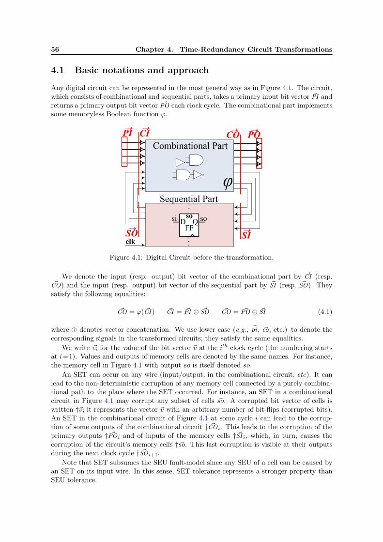
56 Chapter 4. Time-Redundancy Circuit Transformations
4.1 Basic notations and approach
Any digital circuit can be represented in the most general way as in Figure 4.1. The circuit,which consists of combinational and sequential parts, takes a primary input bit vector ~PI andreturns a primary output bit vector ~PO each clock cycle. The combinational part implementssome memoryless Boolean function ϕ.
Sequential Part
Combinational Part
clk
CI COPI
SO SI
φ
si soini:C2FF
D Q
PO
so
Figure 4.1: Digital Circuit before the transformation.
We denote the input (resp. output) bit vector of the combinational part by ~CI (resp.~CO) and the input (resp. output) bit vector of the sequential part by ~SI (resp. ~SO). They
satisfy the following equalities:
~CO = ϕ( ~CI ) ~CI = ~PI ⊕ ~SO ~CO = ~PO ⊕ ~SI (4.1)
where ⊕ denotes vector concatenation. We use lower case (e.g., ~pi , ~co, etc.) to denote thecorresponding signals in the transformed circuits; they satisfy the same equalities.
We write ~vi for the value of the bit vector ~v at the ith clock cycle (the numbering startsat i=1). Values and outputs of memory cells are denoted by the same names. For instance,the memory cell in Figure 4.1 with output so is itself denoted so.
An SET can occur on any wire (input/output, in the combinational circuit, etc). It canlead to the non-deterministic corruption of any memory cell connected by a purely combina-tional path to the place where the SET occurred. For instance, an SET in a combinationalcircuit in Figure 4.1 may corrupt any subset of cells ~so. A corrupted bit vector of cells iswritten †~v; it represents the vector ~v with an arbitrary number of bit-flips (corrupted bits).An SET in the combinational circuit of Figure 4.1 at some cycle i can lead to the corrup-tion of some outputs of the combinational circuit † ~CO i. This leads to the corruption of theprimary outputs † ~PO i and of inputs of the memory cells † ~SI i, which, in turn, causes thecorruption of the circuit’s memory cells †~so. This last corruption is visible at their outputsduring the next clock cycle † ~SO i+1.
Note that SET subsumes the SEU fault-model since any SEU of a cell can be caused byan SET on its input wire. In this sense, SET tolerance represents a stronger property thanSEU tolerance.
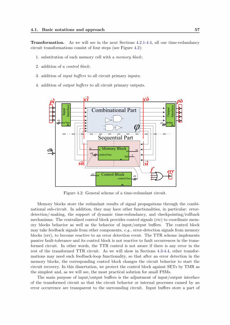
4.1. Basic notations and approach 57
Transformation. As we will see in the next Sections 4.2.1-4.4, all our time-redundancycircuit transformations consist of four steps (see Figure 4.2):
1. substitution of each memory cell with a memory block ;
2. addition of a control block ;
3. addition of input buffers to all circuit primary inputs;
4. addition of output buffers to all circuit primary outputs.
Sequential Part
clk
Combinational Part
ini:C2
Control Block
ini:C2
Memory Blocksi so
failcontrol bus
si soctr
f
control busctr
Inpu
t In
terf
ace
ctr.bus
Out
put
Inte
rfac
e
ctr
ci copi po
so sif
ctr.busctr
φ
errerrerr
Figure 4.2: General scheme of a time-redundant circuit.
Memory blocks store the redundant results of signal propagations through the combi-national sub-circuit. In addition, they may have other functionalities, in particular: error-detection/-making, the support of dynamic time-redundancy, and checkpointing/rollbackmechanisms. The centralized control block provides control signals (ctr) to coordinate mem-ory blocks behavior as well as the behavior of input/output buffers. The control blockmay take feedback signals from other components, e.g., error-detection signals from memoryblocks (err), to become reactive to an error detection event. The TTR scheme implementspassive fault-tolerance and its control block is not reactive to fault occurrences in the trans-formed circuit. In other words, the TTR control is not aware if there is any error in therest of the transformed TTR circuit. As we will show in Sections 4.3-4.4, other transfor-mations may need such feedback-loop functionality, so that after an error detection in thememory blocks, the corresponding control block changes the circuit behavior to start thecircuit recovery. In this dissertation, we protect the control block against SETs by TMR asthe simplest and, as we will see, the most practical solution for small FSMs.
The main purpose of input/output buffers is the adjustment of input/output interfaceof the transformed circuit so that the circuit behavior or internal processes caused by anerror occurrence are transparent to the surrounding circuit. Input buffers store a part of
58 Chapter 4. Time-Redundancy Circuit Transformations
an input stream to provide the necessary information for re-computation in active redun-dant protection mechanisms. Output buffers mask errors and organize a convenient outputinterface.
Any time-redundant transformed circuit requires the upsampling (×N) of the inputstream to organize N-time redundancy. As a result, the kept unchanged combinationalpart is time-multiplexed and the circuit throughput drops at least N-times. Throughput isdefined as the number of significant bits (i.e., those not created by the upsampling) processedper time unit.
4.2 Triple-Time Redundancy
In this section, we present the Triple-Time Redundant Transformation (TTR) for automaticinsertion of SET-masking properties. TTR is a simple technique that provides a good intro-duction to the more advanced time-redundant solutions, presented in Sections 4.3-4.4.
The principle of TTR consists in the multiplexing of the circuits’s combinational partwhen each next state of the original circuit is re-computed three times during three consec-utive clock cycles. It produces three redundant state copies for further majority voting. Asa prerequisite, the input streams have to be upsampled three times.
Since TTR is able to mask soft-errors “on-the-fly”, without any recovery process, it canbe classified as a passive fault-tolerance technique (see Section 2.1.2). The transformedcircuit always returns to its correct state 4 cycles after an SET occurrence and the outputstreams correctness is guaranteed. It allows to state that TTR circuits are tolerant againstthe fault-model “at most one SET within 4 clock cycles”, denoted by SET (1 , 4 ).
We introduce in Section 4.2.1 TTR transformation. Sections 4.2.2-4.2.3 describe thetwo main components of any TTR circuit: the memory block and the control block re-spectively. Section 4.2.4 shows by an informal proof that the transformed TTR circuitsare fault-tolerant w.r.t. the fault-model SET (1 , 4 ). Experimental results using the ITC’99benchmark suite [147] are presented in Section 4.2.6 where we compare the hardware over-head and maximum throughput of TMR and TTR circuits.
4.2.1 Principle of Triple-Time Redundancy
The TTR transformation follows the steps described in Section 4.1. The TTR transformation(see Figure 4.3) requires the triple upsampling (×3) of the input stream. The combinationalpart of the circuit is kept unchanged, as in other time-redundancy transformations, but ϕ(~ci)is computed three times. Since ~pi represents the upsampled primary input bit vector of thetransformed TTR circuit, it satisfies the following equalities:
∀i ∈ N∗. ~pi3i−2 = ~pi3i−1 = ~pi3i = ~PI i (4.2)
A TTR memory block memorizes the values computed by the combinational circuit andperforms voting to mask errors. These memory blocks require additional control signals(fetchA and fetchB) from the control block to schedule these operations.
The TTR scheme implements passive fault-tolerance with no error-detection mechanismnor any form of re-computation after an error detection. Since no additional re-computationis needed, there are no input buffers to keep input stream bits.
Output buffers are also absent because the transformed circuit’s outputs are triplicatedin time and the “surrounding” circuit can mask errors by voting.
The following sections present TTR components in details.
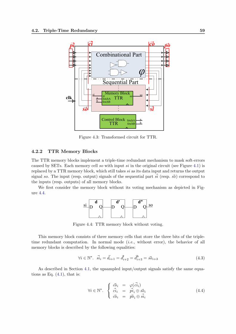
4.2. Triple-Time Redundancy 59
Sequential Part
clk
Combinational Part
ini:C2Control Block fetchA a
fetchB b
Memory Blocksi sofetchAfetchB
si soab
TTR
TTR
ci copi po
φ
siso
Figure 4.3: Transformed circuit for TTR.
4.2.2 TTR Memory Blocks
The TTR memory blocks implement a triple-time redundant mechanism to mask soft-errorscaused by SETs. Each memory cell so with input si in the original circuit (see Figure 4.1) isreplaced by a TTR memory block, which still takes si as its data input and returns the outputsignal so. The input (resp. output) signals of the sequential part ~si (resp. ~so) correspond tothe inputs (resp. outputs) of all memory blocks.
We first consider the memory block without its voting mechanism as depicted in Fig-ure 4.4.
Qd
D Q Qd'
D Qsi Qd'
D Q so'
Figure 4.4: TTR memory block without voting.
This memory block consists of three memory cells that store the three bits of the triple-time redundant computation. In normal mode (i.e., without error), the behavior of allmemory blocks is described by the following equalities:
∀i ∈ N∗. ~si i = ~di+1 = ~d′i+2 = ~d′′i+3 = ~soi+3 (4.3)
As described in Section 4.1, the upsampled input/output signals satisfy the same equa-tions as Eq. (4.1), that is:
∀i ∈ N∗.
~coi = ϕ(~ci i)~ci i = ~pi i ⊕ ~soi~coi = ~poi ⊕ ~si i
(4.4)
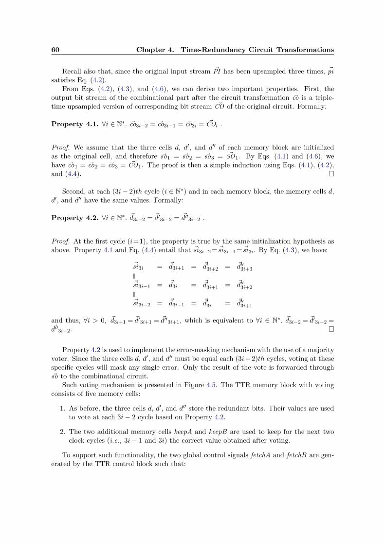
60 Chapter 4. Time-Redundancy Circuit Transformations
Recall also that, since the original input stream ~PI has been upsampled three times, ~pisatisfies Eq. (4.2).
From Eqs. (4.2), (4.3), and (4.6), we can derive two important properties. First, theoutput bit stream of the combinational part after the circuit transformation ~co is a triple-time upsampled version of corresponding bit stream ~CO of the original circuit. Formally:
Property 4.1. ∀i ∈ N∗. ~co3i−2 = ~co3i−1 = ~co3i = ~COi .
Proof. We assume that the three cells d, d′, and d′′ of each memory block are initializedas the original cell, and therefore ~so1 = ~so2 = ~so3 = ~SO1. By Eqs. (4.1) and (4.6), wehave ~co1 = ~co2 = ~co3 = ~CO1. The proof is then a simple induction using Eqs. (4.1), (4.2),and (4.4).
Second, at each (3i− 2)th cycle (i ∈ N∗) and in each memory block, the memory cells d,d′, and d′′ have the same values. Formally:
Property 4.2. ∀i ∈ N∗. ~d3i−2 = ~d′3i−2 = ~d′′3i−2 .
Proof. At the first cycle (i=1), the property is true by the same initialization hypothesis asabove. Property 4.1 and Eq. (4.4) entail that ~si3i−2 = ~si3i−1 = ~si3i. By Eq. (4.3), we have:
~si3i = ~d3i+1 = ~d′3i+2 = ~d′′3i+3
‖~si3i−1 = ~d3i = ~d′3i+1 = ~d′′3i+2
‖~si3i−2 = ~d3i−1 = ~d′3i = ~d′′3i+1
and thus, ∀i > 0, ~d3i+1 = ~d′3i+1 = ~d′′3i+1, which is equivalent to ∀i ∈ N∗. ~d3i−2 = ~d′3i−2 =~d′′3i−2.
Property 4.2 is used to implement the error-masking mechanism with the use of a majorityvoter. Since the three cells d, d′, and d′′ must be equal each (3i−2)th cycles, voting at thesespecific cycles will mask any single error. Only the result of the vote is forwarded through~so to the combinational circuit.
Such voting mechanism is presented in Figure 4.5. The TTR memory block with votingconsists of five memory cells:
1. As before, the three cells d, d′, and d′′ store the redundant bits. Their values are usedto vote at each 3i− 2 cycle based on Property 4.2.
2. The two additional memory cells keepA and keepB are used to keep for the next twoclock cycles (i.e., 3i− 1 and 3i) the correct value obtained after voting.
To support such functionality, the two global control signals fetchA and fetchB are gen-erated by the TTR control block such that:
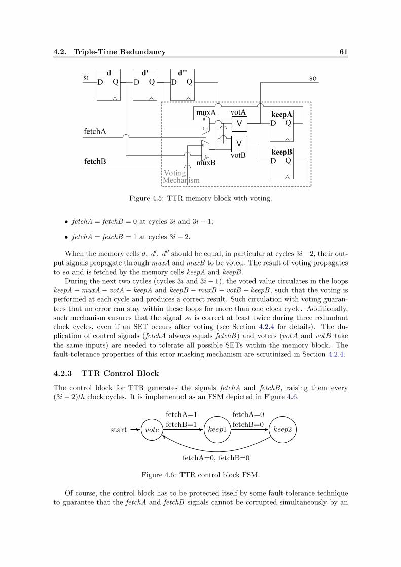
4.2. Triple-Time Redundancy 61
Qd
D Q Qd'
D Q Qd''
D Q
V1
0
C
1
0
C
QkeepAD Q
QkeepBD Q
so
fetchA
fetchB
si
V
muxA
muxB
votA
votB
VotingMechanism
Figure 4.5: TTR memory block with voting.
• fetchA = fetchB = 0 at cycles 3i and 3i− 1;
• fetchA = fetchB = 1 at cycles 3i− 2.
When the memory cells d, d′, d′′ should be equal, in particular at cycles 3i−2, their out-put signals propagate through muxA and muxB to be voted. The result of voting propagatesto so and is fetched by the memory cells keepA and keepB .
During the next two cycles (cycles 3i and 3i− 1), the voted value circulates in the loopskeepA−muxA− votA− keepA and keepB −muxB − votB − keepB , such that the voting isperformed at each cycle and produces a correct result. Such circulation with voting guaran-tees that no error can stay within these loops for more than one clock cycle. Additionally,such mechanism ensures that the signal so is correct at least twice during three redundantclock cycles, even if an SET occurs after voting (see Section 4.2.4 for details). The du-plication of control signals (fetchA always equals fetchB) and voters (votA and votB takethe same inputs) are needed to tolerate all possible SETs within the memory block. Thefault-tolerance properties of this error masking mechanism are scrutinized in Section 4.2.4.
4.2.3 TTR Control Block
The control block for TTR generates the signals fetchA and fetchB , raising them every(3i− 2)th clock cycles. It is implemented as an FSM depicted in Figure 4.6.
votestart keep1 keep2
fetchA=1
fetchB=1
fetchA=0
fetchB=0
fetchA=0, fetchB=0
Figure 4.6: TTR control block FSM.
Of course, the control block has to be protected itself by some fault-tolerance techniqueto guarantee that the fetchA and fetchB signals cannot be corrupted simultaneously by an
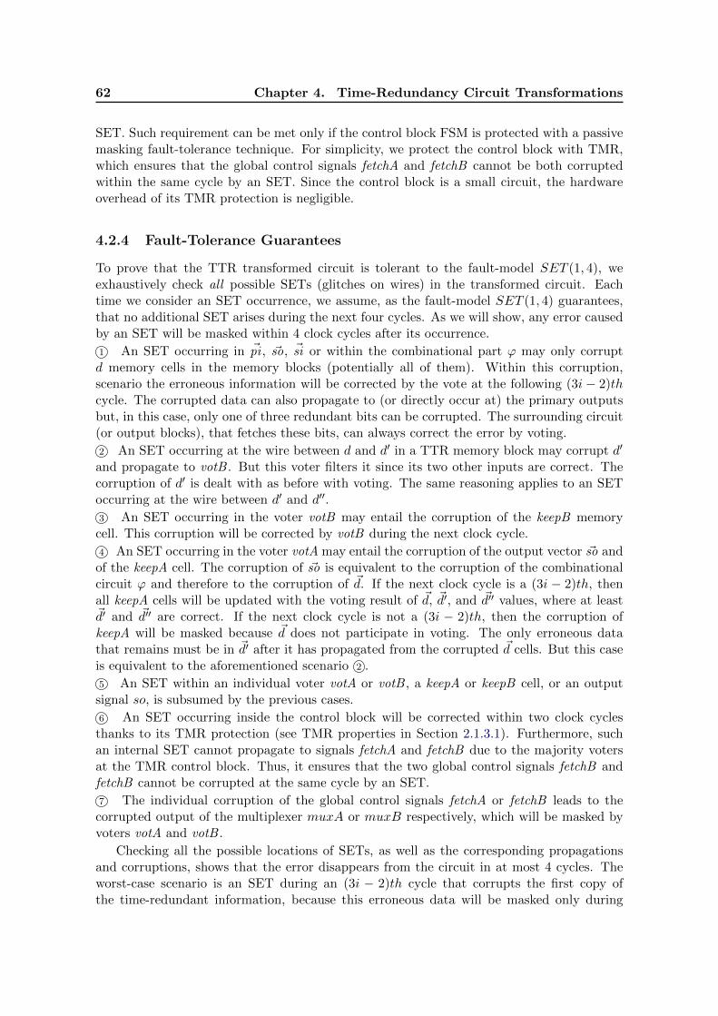
62 Chapter 4. Time-Redundancy Circuit Transformations
SET. Such requirement can be met only if the control block FSM is protected with a passivemasking fault-tolerance technique. For simplicity, we protect the control block with TMR,which ensures that the global control signals fetchA and fetchB cannot be both corruptedwithin the same cycle by an SET. Since the control block is a small circuit, the hardwareoverhead of its TMR protection is negligible.
4.2.4 Fault-Tolerance Guarantees
To prove that the TTR transformed circuit is tolerant to the fault-model SET (1, 4), weexhaustively check all possible SETs (glitches on wires) in the transformed circuit. Eachtime we consider an SET occurrence, we assume, as the fault-model SET (1, 4) guarantees,that no additional SET arises during the next four cycles. As we will show, any error causedby an SET will be masked within 4 clock cycles after its occurrence.
1 An SET occurring in ~pi , ~so, ~si or within the combinational part ϕ may only corruptd memory cells in the memory blocks (potentially all of them). Within this corruption,scenario the erroneous information will be corrected by the vote at the following (3i− 2)thcycle. The corrupted data can also propagate to (or directly occur at) the primary outputsbut, in this case, only one of three redundant bits can be corrupted. The surrounding circuit(or output blocks), that fetches these bits, can always correct the error by voting.
2 An SET occurring at the wire between d and d′ in a TTR memory block may corrupt d′
and propagate to votB . But this voter filters it since its two other inputs are correct. Thecorruption of d′ is dealt with as before with voting. The same reasoning applies to an SEToccurring at the wire between d′ and d′′.
3 An SET occurring in the voter votB may entail the corruption of the keepB memorycell. This corruption will be corrected by votB during the next clock cycle.
4 An SET occurring in the voter votA may entail the corruption of the output vector ~so andof the keepA cell. The corruption of ~so is equivalent to the corruption of the combinationalcircuit ϕ and therefore to the corruption of ~d. If the next clock cycle is a (3i − 2)th, thenall keepA cells will be updated with the voting result of ~d, ~d′, and ~d′′ values, where at least~d′ and ~d′′ are correct. If the next clock cycle is not a (3i − 2)th, then the corruption ofkeepA will be masked because ~d does not participate in voting. The only erroneous datathat remains must be in ~d′ after it has propagated from the corrupted ~d cells. But this caseis equivalent to the aforementioned scenario 2 .
5 An SET within an individual voter votA or votB , a keepA or keepB cell, or an outputsignal so, is subsumed by the previous cases.
6 An SET occurring inside the control block will be corrected within two clock cyclesthanks to its TMR protection (see TMR properties in Section 2.1.3.1). Furthermore, suchan internal SET cannot propagate to signals fetchA and fetchB due to the majority votersat the TMR control block. Thus, it ensures that the two global control signals fetchB andfetchB cannot be corrupted at the same cycle by an SET.
7 The individual corruption of the global control signals fetchA or fetchB leads to thecorrupted output of the multiplexer muxA or muxB respectively, which will be masked byvoters votA and votB .
Checking all the possible locations of SETs, as well as the corresponding propagationsand corruptions, shows that the error disappears from the circuit in at most 4 cycles. Theworst-case scenario is an SET during an (3i − 2)th cycle that corrupts the first copy ofthe time-redundant information, because this erroneous data will be masked only during
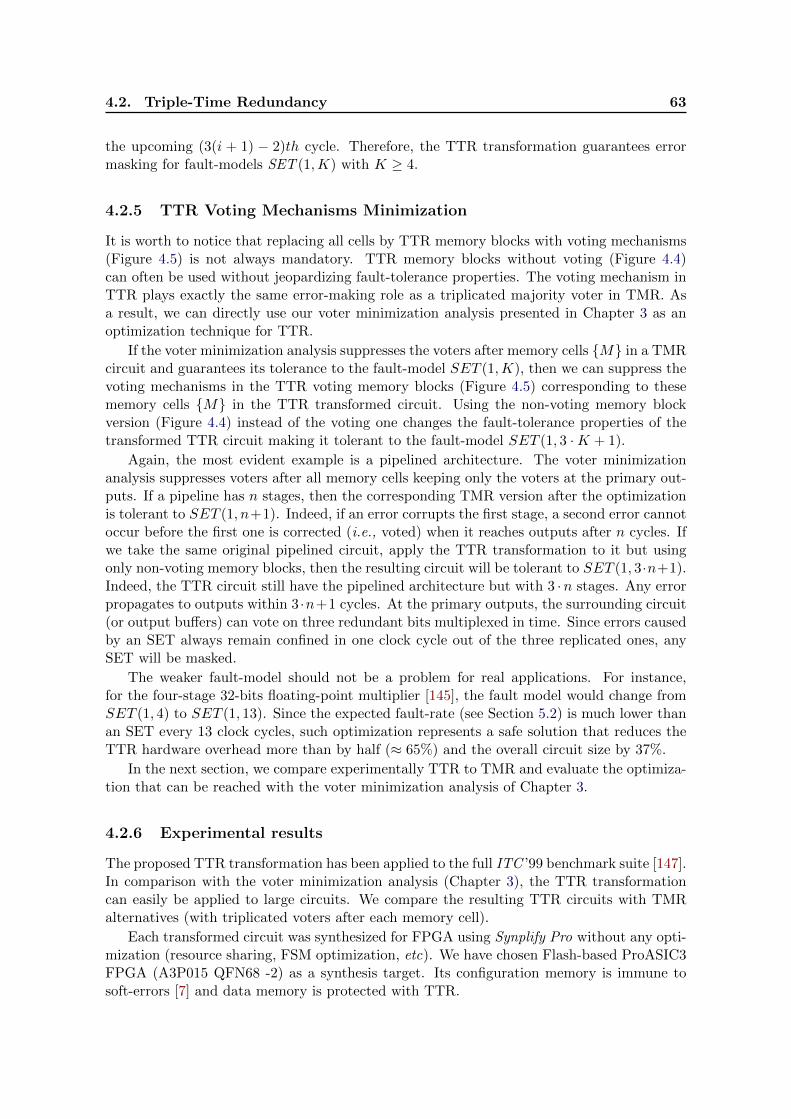
4.2. Triple-Time Redundancy 63
the upcoming (3(i + 1) − 2)th cycle. Therefore, the TTR transformation guarantees errormasking for fault-models SET (1,K) with K ≥ 4.
4.2.5 TTR Voting Mechanisms Minimization
It is worth to notice that replacing all cells by TTR memory blocks with voting mechanisms(Figure 4.5) is not always mandatory. TTR memory blocks without voting (Figure 4.4)can often be used without jeopardizing fault-tolerance properties. The voting mechanism inTTR plays exactly the same error-making role as a triplicated majority voter in TMR. Asa result, we can directly use our voter minimization analysis presented in Chapter 3 as anoptimization technique for TTR.
If the voter minimization analysis suppresses the voters after memory cells {M} in a TMRcircuit and guarantees its tolerance to the fault-model SET (1,K), then we can suppress thevoting mechanisms in the TTR voting memory blocks (Figure 4.5) corresponding to thesememory cells {M} in the TTR transformed circuit. Using the non-voting memory blockversion (Figure 4.4) instead of the voting one changes the fault-tolerance properties of thetransformed TTR circuit making it tolerant to the fault-model SET (1, 3 ·K + 1).
Again, the most evident example is a pipelined architecture. The voter minimizationanalysis suppresses voters after all memory cells keeping only the voters at the primary out-puts. If a pipeline has n stages, then the corresponding TMR version after the optimizationis tolerant to SET (1, n+1). Indeed, if an error corrupts the first stage, a second error cannotoccur before the first one is corrected (i.e., voted) when it reaches outputs after n cycles. Ifwe take the same original pipelined circuit, apply the TTR transformation to it but usingonly non-voting memory blocks, then the resulting circuit will be tolerant to SET (1, 3·n+1).Indeed, the TTR circuit still have the pipelined architecture but with 3 ·n stages. Any errorpropagates to outputs within 3 ·n+1 cycles. At the primary outputs, the surrounding circuit(or output buffers) can vote on three redundant bits multiplexed in time. Since errors causedby an SET always remain confined in one clock cycle out of the three replicated ones, anySET will be masked.
The weaker fault-model should not be a problem for real applications. For instance,for the four-stage 32-bits floating-point multiplier [145], the fault model would change fromSET (1, 4) to SET (1, 13). Since the expected fault-rate (see Section 5.2) is much lower thanan SET every 13 clock cycles, such optimization represents a safe solution that reduces theTTR hardware overhead more than by half (≈ 65%) and the overall circuit size by 37%.
In the next section, we compare experimentally TTR to TMR and evaluate the optimiza-tion that can be reached with the voter minimization analysis of Chapter 3.
4.2.6 Experimental results
The proposed TTR transformation has been applied to the full ITC ’99 benchmark suite [147].In comparison with the voter minimization analysis (Chapter 3), the TTR transformationcan easily be applied to large circuits. We compare the resulting TTR circuits with TMRalternatives (with triplicated voters after each memory cell).
Each transformed circuit was synthesized for FPGA using Synplify Pro without any opti-mization (resource sharing, FSM optimization, etc). We have chosen Flash-based ProASIC3FPGA (A3P015 QFN68 -2) as a synthesis target. Its configuration memory is immune tosoft-errors [7] and data memory is protected with TTR.
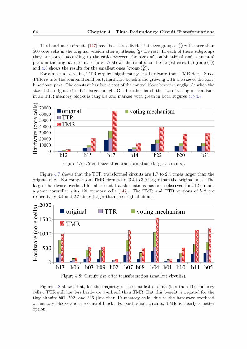
64 Chapter 4. Time-Redundancy Circuit Transformations
The benchmark circuits [147] have been first divided into two groups: 1 with more than500 core cells in the original version after synthesis; 2 the rest. In each of these subgroupsthey are sorted according to the ratio between the sizes of combinational and sequentialparts in the original circuit. Figure 4.7 shows the results for the largest circuits (group 1 )and 4.8 shows the results for the smallest ones (group 2 ).
For almost all circuits, TTR requires significantly less hardware than TMR does. SinceTTR re-uses the combinational part, hardware benefits are growing with the size of the com-binational part. The constant hardware cost of the control block becomes negligible when thesize of the original circuit is large enough. On the other hand, the size of voting mechanismsin all TTR memory blocks is tangible and marked with green in both Figures 4.7-4.8.
b12 b14 b15 b20 b21 b22 b17
010000200003000040000500006000070000
b12)))))))))))))b15))))))))))))b17))))))))))))b14))))))))))))b22))))))))))))b20)))))))))))))b21
originalTTRTMR
voting)mechanism
Har
dwar
e)(c
ore)
cell
s)
Figure 4.7: Circuit size after transformation (largest circuits).
Figure 4.7 shows that the TTR transformed circuits are 1.7 to 2.4 times larger than theoriginal ones. For comparison, TMR circuits are 3.4 to 3.9 larger than the original ones. Thelargest hardware overhead for all circuit transformations has been observed for b12 circuit,a game controller with 121 memory cells [147]. The TMR and TTR versions of b12 arerespectively 3.9 and 2.5 times larger than the original circuit.
0
500
1000
1500
2000
b13wwwwb06wwwwb03wwb09wwwb02wwwwb07wwb08wwwwb04wwwb01wwwb10wwwwb11wwwb05
original TTR
TMR
votingwmechanism
Har
dwar
ew(c
orew
cells
)
Figure 4.8: Circuit size after transformation (smallest circuits).
Figure 4.8 shows that, for the majority of the smallest circuits (less than 100 memorycells), TTR still has less hardware overhead than TMR. But this benefit is negated for thetiny circuits b01, b02, and b06 (less than 10 memory cells) due to the hardware overheadof memory blocks and the control block. For such small circuits, TMR is clearly a betteroption.
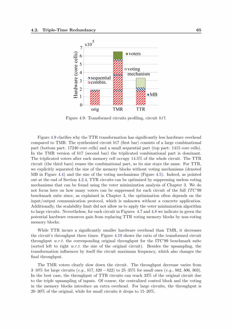
4.2. Triple-Time Redundancy 65
orig TMR TTR
voting5mechanism
MB
voters
sequentialcombin.
Har
dwar
e5(c
ore5
cells
)
0
1
x105
2
3
4
5
6
7
Figure 4.9: Transformed circuits profiling, circuit b17.
Figure 4.9 clarifies why the TTR transformation has significantly less hardware overheadcompared to TMR. The synthesized circuit b17 (first bar) consists of a large combinationalpart (bottom part: 17240 core cells) and a small sequential part (top part: 1415 core cells).In the TMR version of b17 (second bar) the triplicated combinational part is dominant.The triplicated voters after each memory cell occupy 14.5% of the whole circuit. The TTRcircuit (the third bars) reuses the combinational part, so its size stays the same. For TTR,we explicitly separated the size of the memory blocks without voting mechanisms (denotedMB in Figure 4.4) and the size of the voting mechanisms (Figure 4.5). Indeed, as pointedout at the end of Section 4.2.4, TTR circuits can be optimized by suppressing useless votingmechanisms that can be found using the voter minimization analysis of Chapter 3. We donot focus here on how many voters can be suppressed for each circuit of the full ITC ’99benchmark suite since, as explained in Chapter 3, the optimization often depends on theinput/output communication protocol, which is unknown without a concrete application.Additionally, the scalability limit did not allow us to apply the voter minimization algorithmto large circuits. Nevertheless, for each circuit in Figures 4.7 and 4.8 we indicate in green thepotential hardware resources gain from replacing TTR voting memory blocks by non-votingmemory blocks.
While TTR incurs a significantly smaller hardware overhead than TMR, it decreasesthe circuit’s throughput three times. Figure 4.10 shows the ratio of the transformed circuitthroughput w.r.t. the corresponding original throughput for the ITC’99 benchmark suite(sorted left to right w.r.t. the size of the original circuit). Besides the upsampling, thetransformation influences by itself the circuit maximum frequency, which also changes thefinal throughput.
The TMR voters clearly slow down the circuit. The throughput decrease varies from3–10% for large circuits (e.g., b17, b20− b22) to 25–35% for small ones (e.g., b02, b06, b03).In the best case, the throughput of TTR circuits can reach 33% of the original circuit dueto the triple upsampling of inputs. Of course, the centralized control block and the votingin the memory blocks introduce an extra overhead. For large circuits, the throughput is20–30% of the original, while for small circuits it drops to 15–20%.
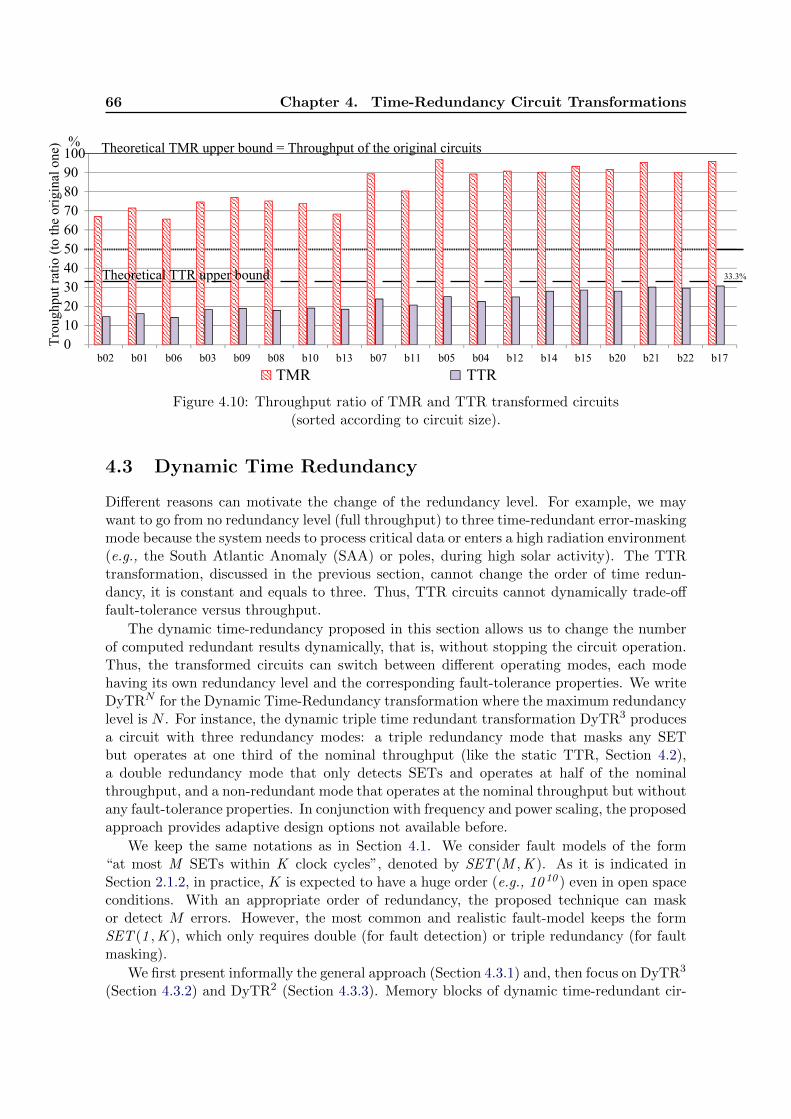
66 Chapter 4. Time-Redundancy Circuit Transformations
b02 b01 b06 b03 b09 b08 b10 b13 b07 b11 b05 b04 b12 b14 b15 b20 b21 b22 b17
Tro
ughp
ut%r
atio
%(to
%the%
orig
inal
%one
)%
Theoretical%TTR%upper%bound% 33.3%
Theoretical%TMR%upper%bound%=%Throughput%of%the%original%circuits%1009080706050403020100
%
TMR TTR
Figure 4.10: Throughput ratio of TMR and TTR transformed circuits(sorted according to circuit size).
4.3 Dynamic Time Redundancy
Different reasons can motivate the change of the redundancy level. For example, we maywant to go from no redundancy level (full throughput) to three time-redundant error-maskingmode because the system needs to process critical data or enters a high radiation environment(e.g., the South Atlantic Anomaly (SAA) or poles, during high solar activity). The TTRtransformation, discussed in the previous section, cannot change the order of time redun-dancy, it is constant and equals to three. Thus, TTR circuits cannot dynamically trade-offfault-tolerance versus throughput.
The dynamic time-redundancy proposed in this section allows us to change the numberof computed redundant results dynamically, that is, without stopping the circuit operation.Thus, the transformed circuits can switch between different operating modes, each modehaving its own redundancy level and the corresponding fault-tolerance properties. We writeDyTRN for the Dynamic Time-Redundancy transformation where the maximum redundancylevel is N . For instance, the dynamic triple time redundant transformation DyTR3 producesa circuit with three redundancy modes: a triple redundancy mode that masks any SETbut operates at one third of the nominal throughput (like the static TTR, Section 4.2),a double redundancy mode that only detects SETs and operates at half of the nominalthroughput, and a non-redundant mode that operates at the nominal throughput but withoutany fault-tolerance properties. In conjunction with frequency and power scaling, the proposedapproach provides adaptive design options not available before.
We keep the same notations as in Section 4.1. We consider fault models of the form“at most M SETs within K clock cycles”, denoted by SET (M ,K ). As it is indicated inSection 2.1.2, in practice, K is expected to have a huge order (e.g., 10 10 ) even in open spaceconditions. With an appropriate order of redundancy, the proposed technique can maskor detect M errors. However, the most common and realistic fault-model keeps the formSET (1 ,K ), which only requires double (for fault detection) or triple redundancy (for faultmasking).
We first present informally the general approach (Section 4.3.1) and, then focus on DyTR3
(Section 4.3.2) and DyTR2 (Section 4.3.3). Memory blocks of dynamic time-redundant cir-

4.3. Dynamic Time Redundancy 67
cuits support the redundancy switching and implement the voting/detection. The globalcontrol block provides signals for controlling the voting and the switching between the avail-able redundancy modes. The input (resp. output) buffers are needed to support the input(resp. output) stream upsampling according to the chosen redundancy order. Experimentalresults using the ITC’99 benchmark suite [147] are presented in Section 4.3.4.
4.3.1 Principle of Dynamic Time Redundancy
Our dynamic time-redundancy transformation DyTRN transforms any circuit at the netlistlevel according to the following steps (see Figure 4.11):
1. choice of the fault-tolerance properties and of the corresponding operating modes;
2. substitution of each original memory cell with a memory block ;
3. addition of a global control block ;
4. adjusting the design of input-output interfaces.
Sequential Part
clk
Combinational Part
ini:C2
Control Block
ini:C2
Memory Blocksi so
failcontrol bus
si soctr
f
control busctr
Inpu
t In
terf
ace
ctr.busO
utpu
t In
terf
ace
ctr
ci copi po
so sif
ctr.busctr
φ
failmod f fail
Figure 4.11: Result of the circuit transformation DyTRN .
The first transformation step is specific for the dynamic time-redundancy transformationsdue to the necessity to choose what fault-tolerance properties are needed. In particular, adesigner can choose:
• the desired error-detection/masking properties (determine existence of error-detectionsignal fail, Figure 4.11);
• the set of needed redundancy levels or operating modes that can guarantee these prop-erties.

68 Chapter 4. Time-Redundancy Circuit Transformations
Qd1
init:C
D Q Qd2
init:C
D Qsi QdN
init:C
D Q
Vot/Detectso
fail
0
1C
modeCtrDynamic2Delay
QdN-1
init:C
D Q... 0
1C
QdN-2
init:C
D Q
...
...1
k
dataA
Saving2Line
dataB
Qdk
init:C
D QQd1~
init:C
D Q ...Qd2
init:C
D Q
~ ~
1 2 m
fetchCtr
...
modeCtr
Figure 4.12: General memory block structure for DyTRN .
For example, an application may ask for either running at full speed (hence no fault-tolerance:N = 1) or being able to detect up to two simultaneous faults (which requires a redundancylevel N = 3). Thus, only two operating modes are needed: mode 1 with no time redundancyand mode 3 with three-time redundancy.
In general terms, the user must choose the set of fault-tolerance properties that aredesired for the resulting circuit. Each property can be either of the form “mask up to ksimultaneous faults” (noted “mask k” for short) or of the form “detect up to k simultaneousfaults” (noted “detect k” for short). When k = 0, both are identical and it means that thecircuit will run at its full throughput.
Recall that detecting (resp. masking) k simultaneous faults requires a redundancy levelof k+1 (resp. 2k+1) minimum. For instance, in five time-redundant mode, we can detect upto four and mask up to two faults, while in the case of four-time redundancy we can detectup to three faults and mask only one.
Accordingly, each property required by the user is then turned into an equivalent oper-ating mode with n redundancy level (noted “mode n” for short). The maximum value ofall those n is the maximum redundancy level of the transformed circuit, noted N , and thecorresponding transformation is written as DyTRN .
To toggle between the chosen redundancy levels, we allocate input control signals ~mod(Figure 4.11) which, set by the surrounding circuit, will define the current operating mode(with the corresponding properties) and support mode switches. The set of available operat-ing modes influences the design of the memory blocks and the control block and, as a result,the hardware size, wiring, and circuit maximum frequency.
4.3.1.1 Memory Blocks
The memory blocks implement the core of the dynamic time-redundant mechanism. Theyrecord the recomputed results and organize the voting and comparison procedures. Theirprecise internal structure depends on the chosen set of operating modes and fault-toleranceproperties.
Each memory cell of the original circuit is replaced by a memory block with the same datainput and output as in all presented time-redundant techniques. The input (resp. output)signals of the sequential part ~si (resp. ~so) correspond to the inputs (resp. outputs) of allmemory blocks (see Figure 4.11). The memory blocks produce a fail signal whenever anerror is detected. An error-detection at any memory block raises the fail primary output,indicating this event to the surrounding circuit. The memory blocks also require additional
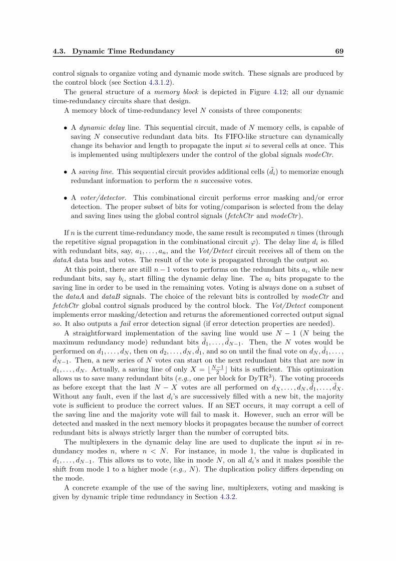
4.3. Dynamic Time Redundancy 69
control signals to organize voting and dynamic mode switch. These signals are produced bythe control block (see Section 4.3.1.2).
The general structure of a memory block is depicted in Figure 4.12; all our dynamictime-redundancy circuits share that design.
A memory block of time-redundancy level N consists of three components:
• A dynamic delay line. This sequential circuit, made of N memory cells, is capable ofsaving N consecutive redundant data bits. Its FIFO-like structure can dynamicallychange its behavior and length to propagate the input si to several cells at once. Thisis implemented using multiplexers under the control of the global signals modeCtr.
• A saving line. This sequential circuit provides additional cells (di) to memorize enoughredundant information to perform the n successive votes.
• A voter/detector. This combinational circuit performs error masking and/or errordetection. The proper subset of bits for voting/comparison is selected from the delayand saving lines using the global control signals (fetchCtr and modeCtr).
If n is the current time-redundancy mode, the same result is recomputed n times (throughthe repetitive signal propagation in the combinational circuit ϕ). The delay line di is filledwith redundant bits, say, a1, . . . , an, and the Vot/Detect circuit receives all of them on thedataA data bus and votes. The result of the vote is propagated through the output so.
At this point, there are still n− 1 votes to performs on the redundant bits ai, while newredundant bits, say bi, start filling the dynamic delay line. The ai bits propagate to thesaving line in order to be used in the remaining votes. Voting is always done on a subset ofthe dataA and dataB signals. The choice of the relevant bits is controlled by modeCtr andfetchCtr global control signals produced by the control block. The Vot/Detect componentimplements error masking/detection and returns the aforementioned corrected output signalso. It also outputs a fail error detection signal (if error detection properties are needed).
A straightforward implementation of the saving line would use N − 1 (N being themaximum redundancy mode) redundant bits d1, . . . , dN−1. Then, the N votes would beperformed on d1, . . . , dN , then on d2, . . . , dN , d1, and so on until the final vote on dN , d1, . . . ,dN−1. Then, a new series of N votes can start on the next redundant bits that are now ind1, . . . , dN . Actually, a saving line of only X = bN−1
2 c bits is sufficient. This optimizationallows us to save many redundant bits (e.g., one per block for DyTR3). The voting proceedsas before except that the last N − X votes are all performed on dX , . . . , dN , d1, . . . , dX .Without any fault, even if the last di’s are successively filled with a new bit, the majorityvote is sufficient to produce the correct values. If an SET occurs, it may corrupt a cell ofthe saving line and the majority vote will fail to mask it. However, such an error will bedetected and masked in the next memory blocks it propagates because the number of correctredundant bits is always strictly larger than the number of corrupted bits.
The multiplexers in the dynamic delay line are used to duplicate the input si in re-dundancy modes n, where n < N . For instance, in mode 1, the value is duplicated ind1, . . . , dN−1. This allows us to vote, like in mode N , on all di’s and it makes possible theshift from mode 1 to a higher mode (e.g., N). The duplication policy differs depending onthe mode.
A concrete example of the use of the saving line, multiplexers, voting and masking isgiven by dynamic triple time redundancy in Section 4.3.2.
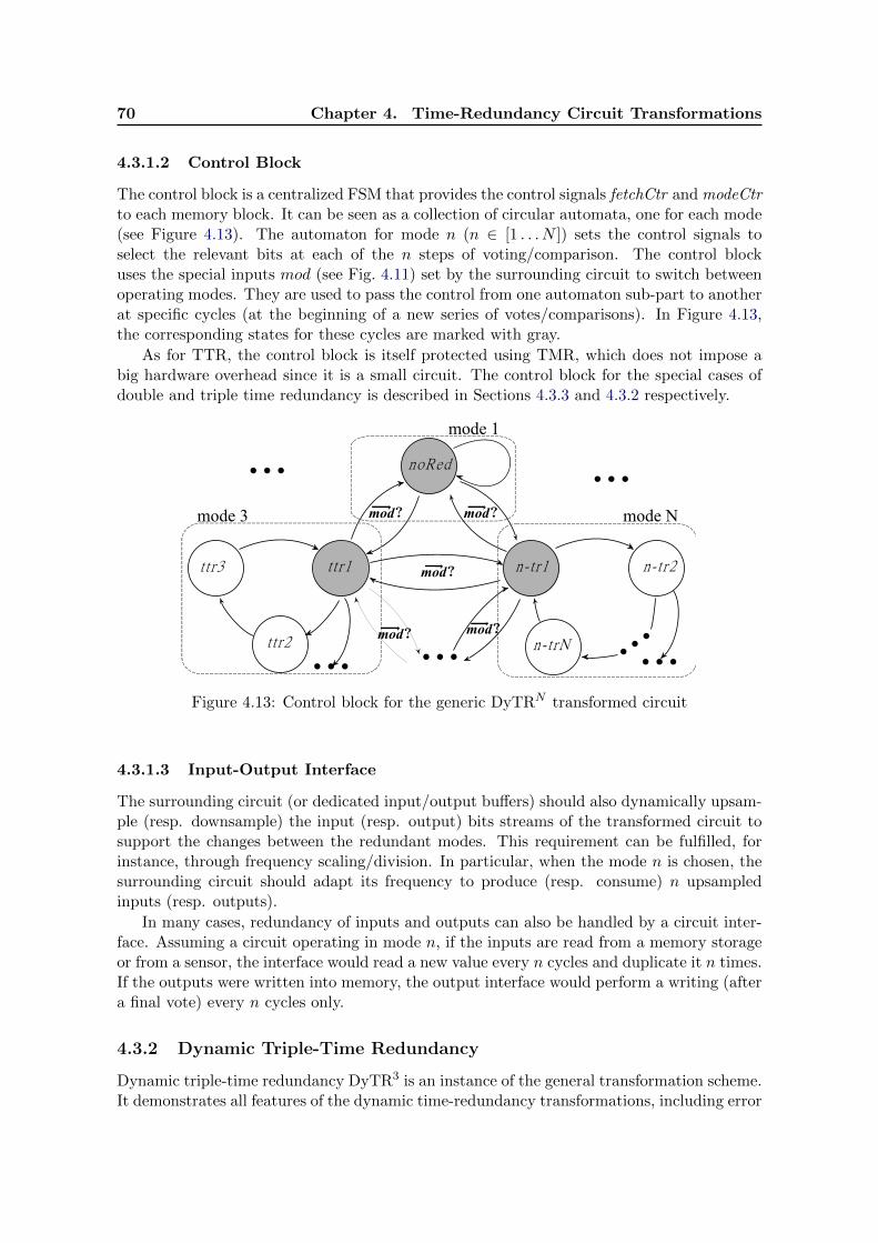
70 Chapter 4. Time-Redundancy Circuit Transformations
4.3.1.2 Control Block
The control block is a centralized FSM that provides the control signals fetchCtr and modeCtrto each memory block. It can be seen as a collection of circular automata, one for each mode(see Figure 4.13). The automaton for mode n (n ∈ [1 . . . N ]) sets the control signals toselect the relevant bits at each of the n steps of voting/comparison. The control blockuses the special inputs mod (see Fig. 4.11) set by the surrounding circuit to switch betweenoperating modes. They are used to pass the control from one automaton sub-part to anotherat specific cycles (at the beginning of a new series of votes/comparisons). In Figure 4.13,the corresponding states for these cycles are marked with gray.
As for TTR, the control block is itself protected using TMR, which does not impose abig hardware overhead since it is a small circuit. The control block for the special cases ofdouble and triple time redundancy is described in Sections 4.3.3 and 4.3.2 respectively.
noRed
tt r3 t t r1
t t r2
n-tr1 n-tr2
n-trN
mode 1
mode 3 mode Nmod
mod
mod
... ...
... modmod... ......Figure 4.13: Control block for the generic DyTRN transformed circuit
4.3.1.3 Input-Output Interface
The surrounding circuit (or dedicated input/output buffers) should also dynamically upsam-ple (resp. downsample) the input (resp. output) bits streams of the transformed circuit tosupport the changes between the redundant modes. This requirement can be fulfilled, forinstance, through frequency scaling/division. In particular, when the mode n is chosen, thesurrounding circuit should adapt its frequency to produce (resp. consume) n upsampledinputs (resp. outputs).
In many cases, redundancy of inputs and outputs can also be handled by a circuit inter-face. Assuming a circuit operating in mode n, if the inputs are read from a memory storageor from a sensor, the interface would read a new value every n cycles and duplicate it n times.If the outputs were written into memory, the output interface would perform a writing (aftera final vote) every n cycles only.
4.3.2 Dynamic Triple-Time Redundancy
Dynamic triple-time redundancy DyTR3 is an instance of the general transformation scheme.It demonstrates all features of the dynamic time-redundancy transformations, including error
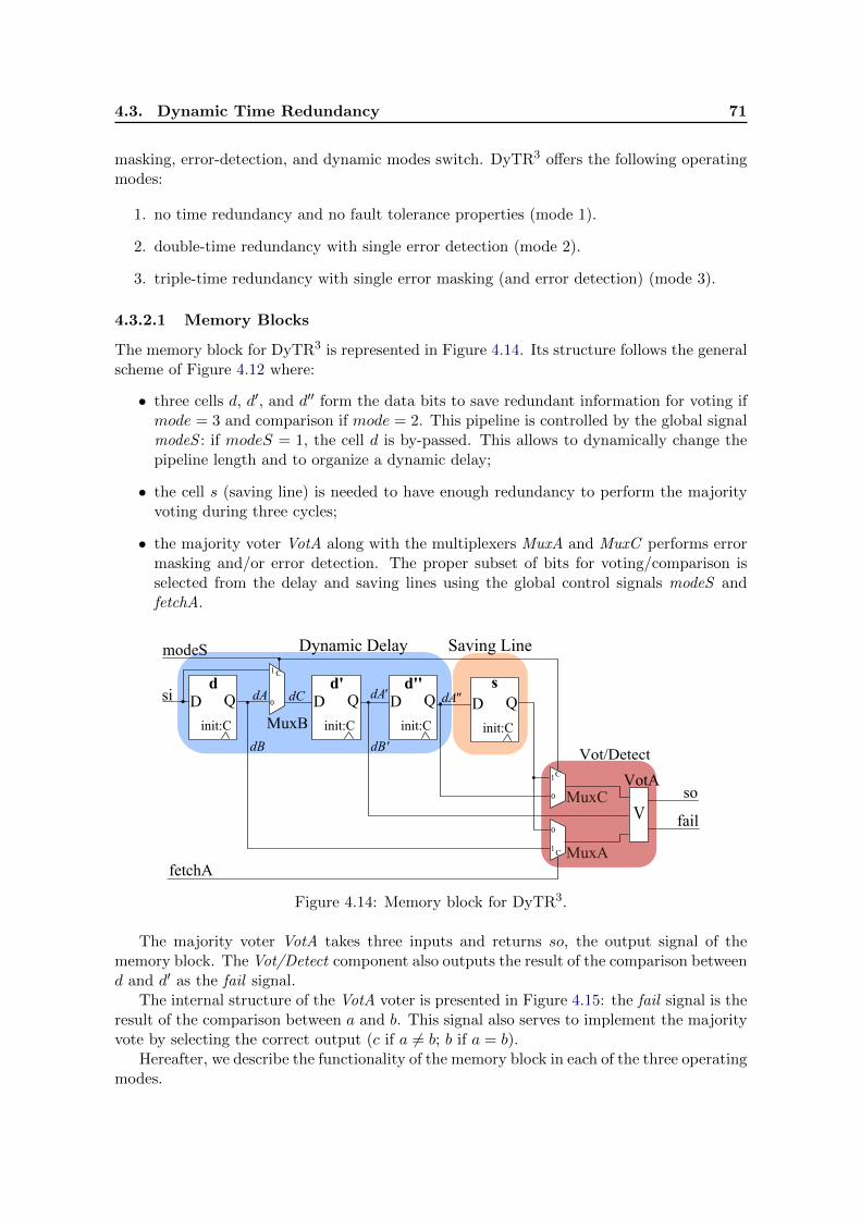
4.3. Dynamic Time Redundancy 71
masking, error-detection, and dynamic modes switch. DyTR3 offers the following operatingmodes:
1. no time redundancy and no fault tolerance properties (mode 1).
2. double-time redundancy with single error detection (mode 2).
3. triple-time redundancy with single error masking (and error detection) (mode 3).
4.3.2.1 Memory Blocks
The memory block for DyTR3 is represented in Figure 4.14. Its structure follows the generalscheme of Figure 4.12 where:
• three cells d, d′, and d′′ form the data bits to save redundant information for voting ifmode = 3 and comparison if mode = 2. This pipeline is controlled by the global signalmodeS : if modeS = 1, the cell d is by-passed. This allows to dynamically change thepipeline length and to organize a dynamic delay;
• the cell s (saving line) is needed to have enough redundancy to perform the majorityvoting during three cycles;
• the majority voter VotA along with the multiplexers MuxA and MuxC performs errormasking and/or error detection. The proper subset of bits for voting/comparison isselected from the delay and saving lines using the global control signals modeS andfetchA.
Qd
init:C
D Q Qd'
init:C
D Qsi dCdA
MuxA
MuxB
Qd''
init:C
D QdA'
V
Q
init:C
D Q
0
1C
so
fail
fetchA
modeS
dB dB'
0
1 C
VotA
Dynamic/Delay Saving/Line
Vot/Detect
s
MuxC0
1C
dA''
Figure 4.14: Memory block for DyTR3.
The majority voter VotA takes three inputs and returns so, the output signal of thememory block. The Vot/Detect component also outputs the result of the comparison betweend and d′ as the fail signal.
The internal structure of the VotA voter is presented in Figure 4.15: the fail signal is theresult of the comparison between a and b. This signal also serves to implement the majorityvote by selecting the correct output (c if a 6= b; b if a = b).
Hereafter, we describe the functionality of the memory block in each of the three operatingmodes.
72 Chapter 4. Time-Redundancy Circuit Transformations
0
1
C
failEQ
≠a
b
cso
Figure 4.15: VotA: voter with detection capability.
Mode 3
In normal execution (i.e., without SET) of the triple-time redundant mode, the behavior ofall memory blocks is described by the following equalities.
In mode 3, the dynamic delay results in:
∀i ∈ N∗. ~si i = ~di+1 = ~d′i+2 = ~d′′i+3 = ~si+4 = ~soi+3 (4.5)
As described in Section 4.1, the upsampled input/output signals satisfy the same equa-tions as Eq. (4.1), that is:
∀i ∈ N∗,
~coi = ϕ(~ci i)~ci i = ~pi i ⊕ ~soi~coi = ~poi ⊕ ~si i
(4.6)
The original input stream ~PI is upsampled three times in this operating mode:
∀i ∈ N∗. ~pi3i−2 = ~pi3i−1 = ~pi3i = ~PI i (4.7)
From Eqs. (4.5), (4.6), and (4.7), we derive that the output bit stream of the combina-tional part after the circuit transformation ~co is a three-times upsampled bit stream ~CO ofthe original circuit.
∀i ∈ N∗. ~co3i−2 = ~co3i−1 = ~co3i = ~CO i (4.8)
In mode 3, the three cells d, d′, and d′′ are equal each (3i− 2)th cycles as formalized byEq. (4.9):
∀i ∈ N∗. ~d3i−2 = ~d′3i−2 = ~d′′3i−2 (4.9)
Voting on (d, d′, d′′) at these specific cycles will mask a single error. The result of thevote is forwarded through ~so to the rest of the combinational circuit. The memory cell s isused to save the value d′′ for the two subsequent votes. Assuming that d, d′, and d′′ holda correct value (say a), the vote at the (3i − 2)th cycle will be between (a, a, a) (storedin (d, d′, d′′)) and at the (3i − 1)th cycle - between (a, a, a) (stored in (d′, d′′, s)). In thiscycle, d contains the next value of the stream (say b), which will propagate to d′. So, thevote at the (3i − 2)th cycle will be between (b, a, a) (stored in (d′, d′′, s)). So, if d′′ or s iscorrupted, the vote may return a wrong value, which will be propagated to the next block.Fortunately, this incorrect value is preceded by two correct ones and can be corrected by aspecial recovery procedure described in details in Section 4.3.2.3. As we will see, such anerror is corrected within the next six clock cycles.
To support this functionality, the global control signal fetchA is generated by the controlblock according to Eq.(4.10).
fetchA = 0 at cycles 3i and 3i− 1
fetchA = 1 at cycles 3i− 2.(4.10)
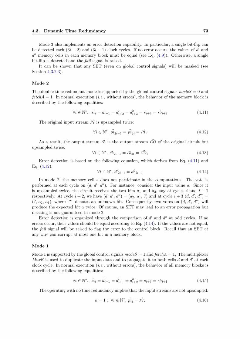
4.3. Dynamic Time Redundancy 73
Mode 3 also implements an error detection capability. In particular, a single bit-flip canbe detected each (3i − 2) and (3i − 1) clock cycles. If no error occurs, the values of d′ andd′′ memory cells in each memory block must be equal (see Eq. (4.9)). Otherwise, a singlebit-flip is detected and the fail signal is raised.
It can be shown that any SET (even on global control signals) will be masked (seeSection 4.3.2.3).
Mode 2
The double-time redundant mode is supported by the global control signals modeS = 0 andfetchA = 1. In normal execution (i.e., without errors), the behavior of the memory block isdescribed by the following equalities:
∀i ∈ N∗. ~si i = ~di+1 = ~d′i+2 = ~d′′i+3 = ~si+4 = ~soi+2 (4.11)
The original input stream ~PI is upsampled twice:
∀i ∈ N∗. ~pi2i−1 = ~pi2i = ~PI i (4.12)
As a result, the output stream ~co is the output stream ~CO of the original circuit butupsampled twice:
∀i ∈ N∗. ~co2i−1 = ~co2i = ~CO i (4.13)
Error detection is based on the following equation, which derives from Eq. (4.11) andEq. (4.12):
∀i ∈ N∗. ~d′2i−1 = ~d′′2i−1 (4.14)
In mode 2, the memory cell s does not participate in the computations. The vote isperformed at each cycle on (d, d′, d′′). For instance, consider the input value a. Since itis upsampled twice, the circuit receives the two bits a1 and a2, say at cycles i and i + 1respectively. At cycle i+ 2, we have (d, d′, d′′) = (a2, a1, ?) and at cycle i+ 3 (d, d′, d′′) =(?, a2, a1), where ’?’ denotes an unknown bit. Consequently, two votes on (d, d′, d′′) willproduce the expected bit a twice. Of course, an SET may lead to an error propagation butmasking is not guaranteed in mode 2.
Error detection is organized through the comparison of d′ and d′′ at odd cycles. If noerrors occur, their values should be equal according to Eq. (4.14). If the values are not equal,the fail signal will be raised to flag the error to the control block. Recall that an SET atany wire can corrupt at most one bit in a memory block.
Mode 1
Mode 1 is supported by the global control signals modeS = 1 and fetchA = 1. The multiplexerMuxB is used to duplicate the input data and to propagate it to both cells d and d′ at eachclock cycle. In normal execution (i.e., without errors), the behavior of all memory blocks isdescribed by the following equalities:
∀i ∈ N∗. ~si i = ~di+1 = ~d′i+1 = ~d′′i+2 = ~si+3 = ~soi+1 (4.15)
The operating with no time redundancy implies that the input streams are not upsampled:
n = 1 : ∀i ∈ N∗. ~pi i = ~PI i (4.16)
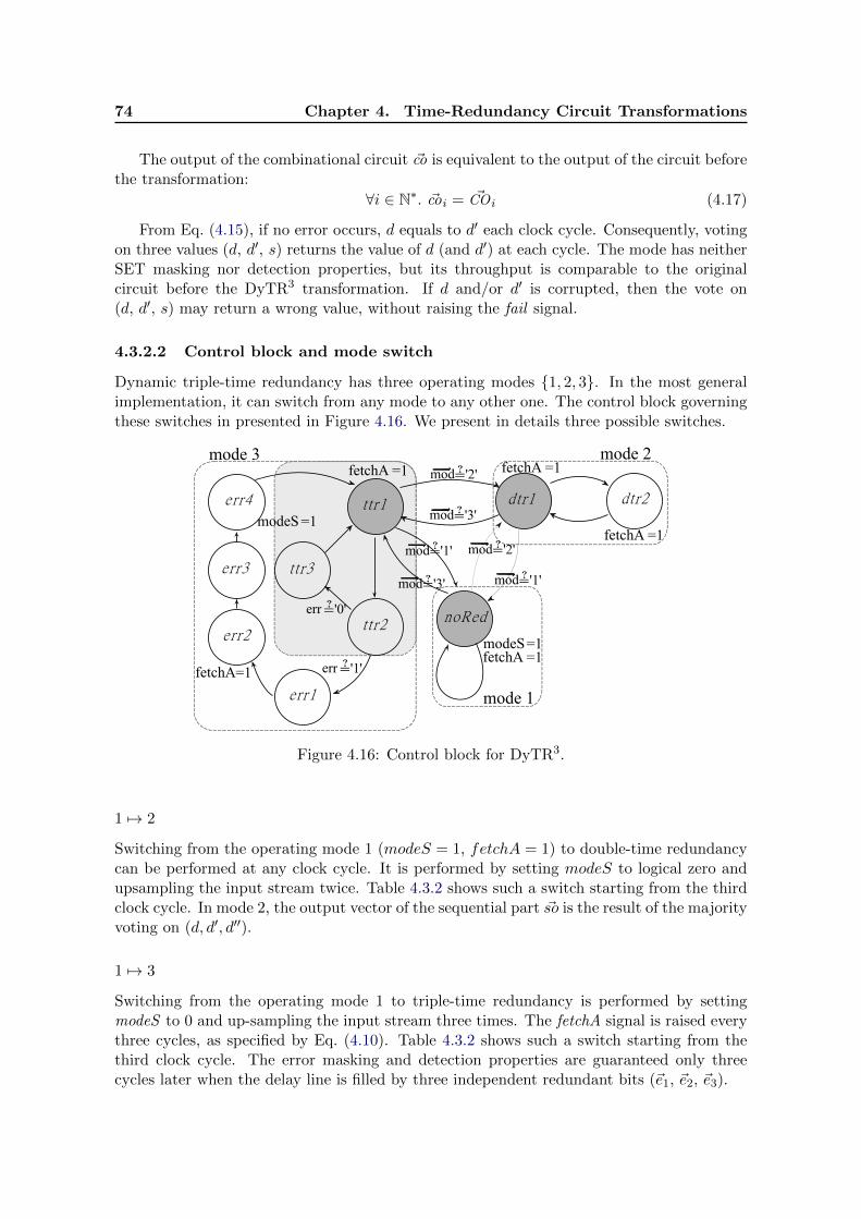
74 Chapter 4. Time-Redundancy Circuit Transformations
The output of the combinational circuit ~co is equivalent to the output of the circuit beforethe transformation:
∀i ∈ N∗. ~coi = ~CO i (4.17)
From Eq. (4.15), if no error occurs, d equals to d′ each clock cycle. Consequently, votingon three values (d, d′, s) returns the value of d (and d′) at each cycle. The mode has neitherSET masking nor detection properties, but its throughput is comparable to the originalcircuit before the DyTR3 transformation. If d and/or d′ is corrupted, then the vote on(d, d′, s) may return a wrong value, without raising the fail signal.
4.3.2.2 Control block and mode switch
Dynamic triple-time redundancy has three operating modes {1, 2, 3}. In the most generalimplementation, it can switch from any mode to any other one. The control block governingthese switches in presented in Figure 4.16. We present in details three possible switches.
t t r3
t t r1
t t r2
dtr1 dtr2
mode 2fetchA =1
fetchA =1
mode 3
'2'mod
'1'mod
noRed
mode 1
modeSfetchA
=1=1
'3'mod
'2'mod
'3'mod
'1'mod
fetchA =1
'0'err
err1
err4
err3
'1'err
err2
fetchA=1
modeS =1
Figure 4.16: Control block for DyTR3.
1 7→ 2
Switching from the operating mode 1 (modeS = 1, fetchA = 1) to double-time redundancycan be performed at any clock cycle. It is performed by setting modeS to logical zero andupsampling the input stream twice. Table 4.3.2 shows such a switch starting from the thirdclock cycle. In mode 2, the output vector of the sequential part ~so is the result of the majorityvoting on (d, d′, d′′).
1 7→ 3
Switching from the operating mode 1 to triple-time redundancy is performed by settingmodeS to 0 and up-sampling the input stream three times. The fetchA signal is raised everythree cycles, as specified by Eq. (4.10). Table 4.3.2 shows such a switch starting from thethird clock cycle. The error masking and detection properties are guaranteed only threecycles later when the delay line is filled by three independent redundant bits (~e1, ~e2, ~e3).

4.3. Dynamic Time Redundancy 75
Table 4.3.2: Switching process 1 7→ 2.
mode clk ~si ~d ~d′ ~d′′ ~s modeS fetchA ~so state
1 1 ~c1~b1 ~b1 ~a1 ~z1 1 1 ~bv noRed
2 ~d1 ~c1 ~c1~b1 ~a1 1 1 ~cv noRed
2 3 ~e1~d1
~d1 ~c1~b1 0 1 ~dv dtr1
4 ~e2 ~e1~d1
~d1 ~c1 0 1 ~dv dtr2
5 ~f1 ~e2 ~e1~d1
~d1 0 1 ~ev dtr1
6 ~f2~f1 ~e2 ~e1
~d1 0 1 ~ev dtr2
7 ~g1~f2
~f1 ~e2 ~e1 0 1 ~fv dtr1
8 ~g2 ~g1~f2
~f1 ~e2 0 1 ~fv dtr2
9 ~h1 ~g2 ~g1~f2
~f1 0 1 ~gv dtr1
xv is the result of voting on the values marked in grey at this clock cycle.
Table 4.3.2: Switching process 1 7→ 3.
mode clk ~si ~d ~d′ ~d′′ ~s modeS fetchA ~so state
1 1 ~c1~b1 ~b1 ~a1 ~z1 1 1 ~bv noRed
2 ~d1 ~c1 ~c1~b1 ~a1 1 1 ~cv noRed
3 3 ~e1~d1
~d1 ~c1~b1 0 1 ~dv ttr1
4 ~e2 ~e1~d1
~d1 ~c1 0 0 ~dv ttr2
5 ~e3 ~e2 ~e1~d1
~d1 0 0 ~dv ttr3
6 ~f1 ~e3 ~e2 ~e1~d1 0 1 ~ev ttr1
7 ~f2~f1 ~e3 ~e2 ~e1 0 0 ~ev ttr2
8 ~f3~f2
~f1 ~e3 ~e2 0 0 ~ev ttr3
9 ~g1~f3
~f2~f1 ~e3 0 1 ~fv ttr1
xv is the result of voting on the values marked in grey at this clock cycle.
76 Chapter 4. Time-Redundancy Circuit Transformations
Table 4.3.2: Switching process 3 7→ 1.
mode clk ~si ~d ~d′ ~d′′ ~s mS fA ~so state
3 1 ~h2~h1 ~g3 ~g2 ~g1 0 0 ~gv ttr2
2 ~h3~h2
~h1 ~g3 ~g2 0 0 ~gv ttr3
3 ~j1 ~h3~h2
~h1 ~g3 0 1 ~hv ttr1
4 ~j2 ~j1 ~h3~h2
~h1 0 0 ~hv ttr2
5 ~j3 ~j2 ~j1 ~h3~h2 0 0 ~hv ttr3
6 ~k1~j3 ~j2 ~j1 ~h3 0 1 ~jv ttr1
1 7 ~l1 ~k1~k1
~j2 ~j1 1 1 ~kv noRed
8 ~m1~l1 ~l1 ~k1
~j2 1 1 ~lv noRed
9 ~n1 ~m2 ~m1~l1 ~k1 1 1 ~mv noRed
xv is the result of voting on the values marked in grey at this clock cycle; mS = modeS ;fA = fetchA.
3 7→ 1
Switching from three times redundancy to non-redundant mode is performed by raisingsignals modeS and fetchA. In Table 4.3.2, this switching is performed at the seventh clockcycle.
All other switching scenarios are supported by the DyTR3 control block as shown inFigure 4.16. Each circular automaton part corresponds to one of the three available operatingmodes.
The labels specify the values of the global control signals (when absent from a state theyare supposed to be 0). The guard mod is the primary input bus that the environment mayuse to indicate which mode switch must be performed. In each operating mode, there is onlyone state allowing a switch. This state ensures that the output stream is consistent (i.e., isnot “cut” in the middle of a redundant series). For example, when switching from mode 3to 1, the output stream has only triplicated values (when in mode 3) followed by single ones(when in mode 1).
The automaton corresponding to mode 3 has two circular sub-parts: ttr1 − ttr2 − ttr3and ttr1− ttr2− err1− err2− err3− err4. The former corresponds to the functionality ifno soft errors have been detected. The latter is used if the fail signal is raised by Vot/Detectduring any 3i− 1 clock cycle (state ttr2 of the control block), indicating a data corruption.The recovery procedure corresponding to this case is described in the next section.
4.3.2.3 Fault tolerance guarantees
In this section, we show that a DyTR3 circuit in triple-time redundant operating mode(mode 3) is able to mask the effect of any SET within six cycles after its occurrence. In otherwords, it is fault-tolerant w.r.t. the SET (1, 7) fault model. The fault-tolerance properties ofmode 2 can be checked with the same reasoning and mode 1 does not have any fault-toleranceproperties.
The error-masking properties are again based on the fact that, even if a single SET cancorrupt several memory blocks, it can corrupt only one cell in a given memory block. Indeed,in mode 3, in the normal operating mode, the signal modeS is equal to 0, hence an SET at
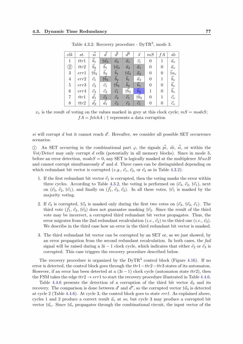
4.3. Dynamic Time Redundancy 77
Table 4.3.2: Recovery procedure - DyTR3, mode 3.
clk st. ~si ~d ~d′ ~d′′ ~s mS fA ~so
1 ttr1 ~b1 †~a3 ~a2 ~a1 ~z1 0 1 ~av2 ttr2 ~b2 ~b1 †~a3 ~a2 ~a1 0 0 ~av3 err1 †~b3 ~b2 ~b1 †~a3 ~a2 0 0 ~†av4 err2 ~c1 †~b3 ~b2 ~b1 ~a3 0 1 ~bv5 err3 ~c2 ~c1 †~b3 ~b2 ~b1 0 0 ~bv6 err4 ~c3 ~c2 ~c1 †~b3 ~b2 1 0 ~bv7 ttr1 ~d1 ~c3 ~c2 ~c1 †~b3 0 1 ~cv8 ttr2 ~d2
~d1 ~c3 ~c2 ~c1 0 0 ~cv
xv is the result of voting on the values marked in grey at this clock cycle; mS = modeS ;fA = fetchA ; † represents a data corruption
si will corrupt d but it cannot reach d′. Hereafter, we consider all possible SET occurrencescenarios.
1 An SET occurring in the combinational part ϕ, the signals ~pi , ~so, ~si , or within theVot/Detect may only corrupt d cells (potentially in all memory blocks). Since in mode 3,before an error detection, modeS = 0, any SET is logically masked at the multiplexer MuxBand cannot corrupt simultaneously d′ and d. Three cases can be distinguished depending onwhich redundant bit vector is corrupted (e.g., ~e1, ~e2, or ~e3 as in Table 4.3.2):
1. If the first redundant bit vector ~e1 is corrupted, then the voting masks the error withinthree cycles. According to Table 4.3.2, the voting is performed on (~e3, ~e2, †~e1), nexton (~e3, ~e2, †~e1), and finally on (~f1, ~e3, ~e2). In all these votes, †~e1 is masked by themajority voting.
2. If ~e2 is corrupted, †~e2 is masked only during the first two votes on (~e3, †~e2, ~e1). Thethird vote (~f1, ~e3, †~e2) does not guarantee masking †~e2. Since the result of the thirdvote may be incorrect, a corrupted third redundant bit vector propagates. Thus, theerror migrates from the 2nd redundant recalculation (i.e., ~e2) to the third one (i.e., ~e3).We describe in the third case how an error in the third redundant bit vector is masked.
3. The third redundant bit vector can be corrupted by an SET or, as we just showed, byan error propagation from the second redundant recalculation. In both cases, the failsignal will be raised during a 3i− 1 clock cycle, which indicates that either ~e2 or ~e3 iscorrupted. This case triggers the recovery procedure described below.
The recovery procedure is organized by the DyTR3 control block (Figure 4.16). If noerror is detected, the control block goes through the ttr1−ttr2−ttr3 states of its automaton.However, if an error has been detected at a (3i− 1) clock cycle (automaton state ttr2), thenthe FSM takes the edge ttr2→ err1 to start the recovery procedure illustrated in Table 4.4.6.
Table 4.4.6 presents the detection of a corruption of the third bit vector ~a3 and itsrecovery. The comparison is done between d′ and d′′, so the corrupted vector †~a3 is detectedat cycle 2 (Table 4.4.6). At cycle 3, the control block goes to state err1. As explained above,cycles 1 and 2 produce a correct result ~av at so, but cycle 3 may produce a corrupted bitvector †~av. Since †~av propagates through the combinational circuit, the input vector of the
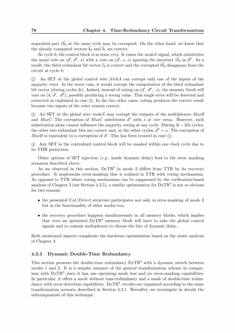
78 Chapter 4. Time-Redundancy Circuit Transformations
sequential part †~b3 at the same cycle may be corrupted. On the other hand, we know thatthe already computed vectors ~b2 and ~b1 are correct.
At cycle 6, the control block is in state err4. It raises the modeS signal, which substitutesthe usual vote on (d′, d′′, s) with a vote on (d′, s, s) ignoring the incorrect †~b3 in d′′. As aresult, the third redundant bit vector ~c3 is correct and the corrupted †~b3 disappears from thecircuit at cycle 8.
2 An SET at the global control wire fetchA can corrupt only one of the inputs of themajority voter. In the worst case, it would corrupt the computation of the third redundantbit vector (during cycles 3i). Indeed, instead of voting on (d′, d′′, s), the memory block willvote on (d, d′, d′′), possibly producing a wrong value. This single error will be detected andcorrected as explained in case 1 . In the two other cases, voting produces the correct resultbecause two inputs of the voter remain correct.
3 An SET at the global wire modeS may corrupt the outputs of the multiplexers MuxBand MuxC. The corruption of MuxC substitutes d′′ with s or vice versa. However, suchsubstitution alone cannot influence the majority voting at any cycle. During 3i− 2th cycles,the other two redundant bits are correct and, at the other cycles, d′′ = s. The corruption ofMuxB is equivalent to a corruption of d′. This has been treated in case 1 .
4 Any SET in the centralized control block will be masked within one clock cycle due toits TMR protection.
Other options of SET injection (e.g., inside dynamic delay) lead to the error maskingscenarios described above.
As we observed in this section, DyTR3 in mode 3 differs from TTR by its recoveryprocedure. It implements error-masking that is realized in TTR with voting mechanisms.As opposed to TTR where voting mechanisms can be suppressed by the verification-basedanalysis of Chapter 3 (see Section 4.2.5), a similar optimization for DyTR3 is not so obviousfor two reasons:
• the presented V ot/Detect structure participates not only in error-masking of mode 3but in the functionality of other modes too;
• the recovery procedure happens simultaneously in all memory blocks, which impliesthat even an optimized DyTR3 memory block will have to take the global controlsignals and to contain multiplexers to choose the bits of dynamic delay.
Both mentioned aspects complicate the hardware optimization based on the static analysisof Chapter 3.
4.3.3 Dynamic Double-Time Redundancy
This section presents the double-time redundancy DyTR2 with a dynamic switch betweenmodes 1 and 2. It is a simpler instance of the general transformation scheme in compar-ison with DyTR3 since it has one operating mode less and no error-masking capabilities.In particular, it offers a mode without time-redundancy and a mode of double-time redun-dancy with error-detection capabilities. DyTR2 circuits are organized according to the sametransformation scenario described in Section 4.3.1. Hereafter, we investigate in details thesubcomponents of this technique.
4.3. Dynamic Time Redundancy 79
4.3.3.1 Memory Blocks
In dynamic double-time redundancy, error masking is fundamentally impossible becausethere is not enough redundancy. Consequently, DyTR2 memory blocks (Figure 4.17) haveonly error detection capabilities. A DyTR2 memory block includes the comparator EQ todetect soft-errors caused by an SET as well as the multiplexer MUX to switch-off timeredundancy.
Dynamic Delay
Qd
D Q Qd'
D Qsi
modeS
fail
1
0C
soMUX
EQ
≠
Vot/Detect
Figure 4.17: Memory Block for DyTR2.
The memory block for DyTR2 consists of the following components:
• two cells d and d′ (the data bits) to save redundant information for comparison inmode 2; in this operating mode, the input stream is upsampled twice and d and d′
contain the same value each odd cycle. For example, if the input stream leads tosi1=a, si2=a, si2=b,... then the pair (d, d′) will contain successively the values (0, 0),(a, 0), (a, a), (b, a), . . . where the initial values of the cells are supposed to be 0;
• a comparator EQ which raises the fail signal if d and d′ differ; in mode 2, if this signalis raised during an odd cycle, it indicates an error detection;
• a multiplexer MUX that allows to switch between the double-time redundancy (mode 2when modeS=0) and no redundancy (mode 1 when modeS=1); it is used to by-passthe d′ memory cell; in this case, the circuit throughput is twice higher than in mode2 but faults cannot be detected; the modeS signal is a global control wire provided bythe control block.
Compared to the general representation of memory blocks (Figure 4.12), the memorycells d and d′ represents the dynamic delay part, while the comparator EQ along with themultiplexer MUX play the role of the Vot/Detect sub-circuit. The saving line is not neededby this transformation because of the absence of voting and error-masking properties. Thereis no need to keep the redundant information in saving line for consecutive voting as it isdone in DyTR3. Since there are only two DyTR2 operating modes, the choice between themcan be done by a single control wire (modeS ) in comparison with DyTR3 that requires twowires (modeS and fetchA) to choose between its three modes.
4.3.3.2 Control block and mode switch
While the functionality of the memory block is straightforward, the switching process needsto be detailed. With double-time redundancy only two switches are possible: from no re-dundancy to double-time (1 7→ 2) and back (2 7→ 1). Table 4.3.3 presents a generic exampleof an execution of twelve cycles with two successive switches (1 7→ 2 and then 2 7→ 1).
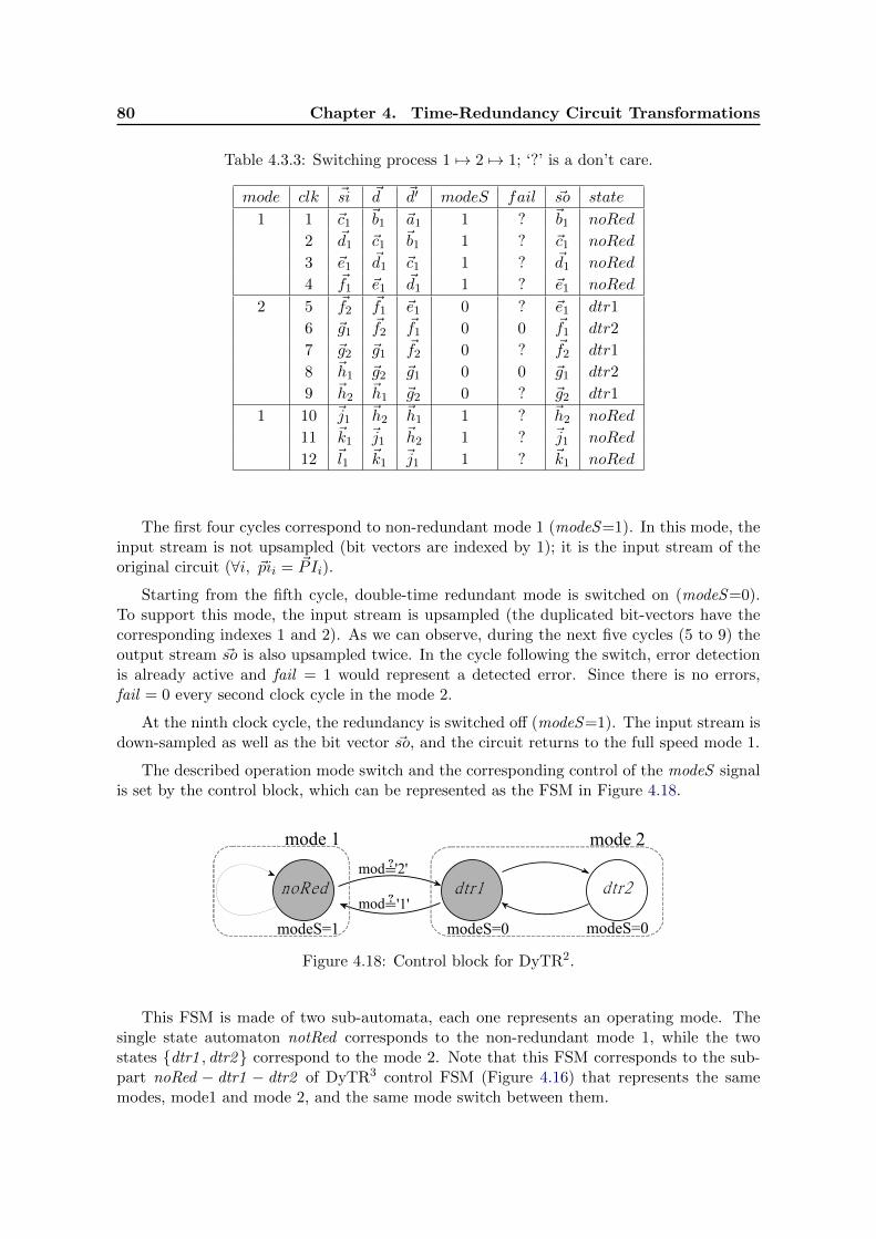
80 Chapter 4. Time-Redundancy Circuit Transformations
Table 4.3.3: Switching process 1 7→ 2 7→ 1; ‘?’ is a don’t care.
mode clk ~si ~d ~d′ modeS fail ~so state
1 1 ~c1~b1 ~a1 1 ? ~b1 noRed
2 ~d1 ~c1~b1 1 ? ~c1 noRed
3 ~e1~d1 ~c1 1 ? ~d1 noRed
4 ~f1 ~e1~d1 1 ? ~e1 noRed
2 5 ~f2~f1 ~e1 0 ? ~e1 dtr1
6 ~g1~f2
~f1 0 0 ~f1 dtr2
7 ~g2 ~g1~f2 0 ? ~f2 dtr1
8 ~h1 ~g2 ~g1 0 0 ~g1 dtr2
9 ~h2~h1 ~g2 0 ? ~g2 dtr1
1 10 ~j1 ~h2~h1 1 ? ~h2 noRed
11 ~k1~j1 ~h2 1 ? ~j1 noRed
12 ~l1 ~k1~j1 1 ? ~k1 noRed
The first four cycles correspond to non-redundant mode 1 (modeS=1). In this mode, theinput stream is not upsampled (bit vectors are indexed by 1); it is the input stream of theoriginal circuit (∀i, ~pii = ~PIi).
Starting from the fifth cycle, double-time redundant mode is switched on (modeS=0).To support this mode, the input stream is upsampled (the duplicated bit-vectors have thecorresponding indexes 1 and 2). As we can observe, during the next five cycles (5 to 9) theoutput stream ~so is also upsampled twice. In the cycle following the switch, error detectionis already active and fail = 1 would represent a detected error. Since there is no errors,fail = 0 every second clock cycle in the mode 2.
At the ninth clock cycle, the redundancy is switched off (modeS=1). The input stream isdown-sampled as well as the bit vector ~so, and the circuit returns to the full speed mode 1.
The described operation mode switch and the corresponding control of the modeS signalis set by the control block, which can be represented as the FSM in Figure 4.18.
noRed
mode 1
dtr1 dtr2
mode 2
modeS=1
mod '2'
'1'mod
modeS=0 modeS=0
Figure 4.18: Control block for DyTR2.
This FSM is made of two sub-automata, each one represents an operating mode. Thesingle state automaton notRed corresponds to the non-redundant mode 1, while the twostates {dtr1 , dtr2} correspond to the mode 2. Note that this FSM corresponds to the sub-part noRed − dtr1 − dtr2 of DyTR3 control FSM (Figure 4.16) that represents the samemodes, mode1 and mode 2, and the same mode switch between them.
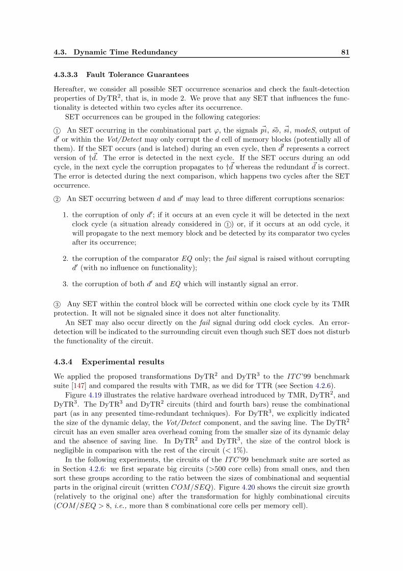
4.3. Dynamic Time Redundancy 81
4.3.3.3 Fault Tolerance Guarantees
Hereafter, we consider all possible SET occurrence scenarios and check the fault-detectionproperties of DyTR2, that is, in mode 2. We prove that any SET that influences the func-tionality is detected within two cycles after its occurrence.
SET occurrences can be grouped in the following categories:
1 An SET occurring in the combinational part ϕ, the signals ~pi , ~so, ~si , modeS, output ofd′ or within the Vot/Detect may only corrupt the d cell of memory blocks (potentially all ofthem). If the SET occurs (and is latched) during an even cycle, then ~d′ represents a correctversion of †~d. The error is detected in the next cycle. If the SET occurs during an oddcycle, in the next cycle the corruption propagates to †~d whereas the redundant ~d is correct.The error is detected during the next comparison, which happens two cycles after the SEToccurrence.
2 An SET occurring between d and d′ may lead to three different corruptions scenarios:
1. the corruption of only d′; if it occurs at an even cycle it will be detected in the nextclock cycle (a situation already considered in 1 ) or, if it occurs at an odd cycle, itwill propagate to the next memory block and be detected by its comparator two cyclesafter its occurrence;
2. the corruption of the comparator EQ only; the fail signal is raised without corruptingd′ (with no influence on functionality);
3. the corruption of both d′ and EQ which will instantly signal an error.
3 Any SET within the control block will be corrected within one clock cycle by its TMRprotection. It will not be signaled since it does not alter functionality.
An SET may also occur directly on the fail signal during odd clock cycles. An error-detection will be indicated to the surrounding circuit even though such SET does not disturbthe functionality of the circuit.
4.3.4 Experimental results
We applied the proposed transformations DyTR2 and DyTR3 to the ITC ’99 benchmarksuite [147] and compared the results with TMR, as we did for TTR (see Section 4.2.6).
Figure 4.19 illustrates the relative hardware overhead introduced by TMR, DyTR2, andDyTR3. The DyTR3 and DyTR2 circuits (third and fourth bars) reuse the combinationalpart (as in any presented time-redundant techniques). For DyTR3, we explicitly indicatedthe size of the dynamic delay, the Vot/Detect component, and the saving line. The DyTR2
circuit has an even smaller area overhead coming from the smaller size of its dynamic delayand the absence of saving line. In DyTR2 and DyTR3, the size of the control block isnegligible in comparison with the rest of the circuit (< 1%).
In the following experiments, the circuits of the ITC ’99 benchmark suite are sorted asin Section 4.2.6: we first separate big circuits (>500 core cells) from small ones, and thensort these groups according to the ratio between the sizes of combinational and sequentialparts in the original circuit (written COM/SEQ). Figure 4.20 shows the circuit size growth(relatively to the original one) after the transformation for highly combinational circuits(COM/SEQ > 8, i.e., more than 8 combinational core cells per memory cell).

82 Chapter 4. Time-Redundancy Circuit Transformations
bsavingblinen
Vot/DetectH
ardw
areb
(cor
ebce
lls)
30
25
20
15
10
5
0
voters
Dyn.Delay
sequentialcombin.
Ctr.Block
DyTR DyTRTMRoriginal 23
x103
Figure 4.19: Transformed circuits profiling (circuit b21 ).
70x103
originalTMR
DyTRDyTR
0102030405060
3
2
b12 b15 b17 b14 b22 b20 b21
Har
dwar
e (c
ore
cells
)
Figure 4.20: Circuit size after transformation, big circuits (for all COM/SEQ > 8).
Figure 4.20 shows that the DyTR2 circuits are 1.18 to 1.37 times larger than the originalones, whereas DyTR3 circuits are 1.46 to 2.17 times larger. For comparison, TMR circuitsare 3.4 to 3.9 times larger than the original ones. As a result, DyTR2 and DyTR3 circuitsare 2.7 to 2.9 and 1.7 to 2.4 smaller than TMR ones.
Figure 4.21 shows that when the combinational part is small, DyTR2 and DyTR3 arestill 2.4 to 2.8 and 1.36 to 1.71 smaller on average than TMR. However, the attractiveness oftime-redundancy schemes is lower for circuits that have small combinational parts (e.g., b01,b02, b03, and b06). For such circuits, lower hardware benefits and loss in throughput makesthe non-adaptive TMR a better option.
The figures do not represent the overhead of the input/output interface, which are re-sponsible for streams upsampling/dowsampling respectively. Since such interfaces need tobe tuned to the surrounding circuit, we do not propose a particular design here. The over-all overhead of such interface depends on the number of inputs/outputs wires since a smallupsampling/downsampling FSM may have to be inserted for each of them. For instance,an FSM that upsamples twice a signal can contain one memory cell (with an enable signal)to keep a data bit and a shared two-state counter (one cell and an inverter). For the tripleupsampling (e.g., for DyTR3) we need a three-states counter (two memory cells and 1-2gates) to make cells with enable signals sending the same saved bit three times. Consider,for instance, the circuit b21 with 54 inputs reading some sensor. Each input would requireone of the aforementioned input buffers. The size of an input buffer remains small and we
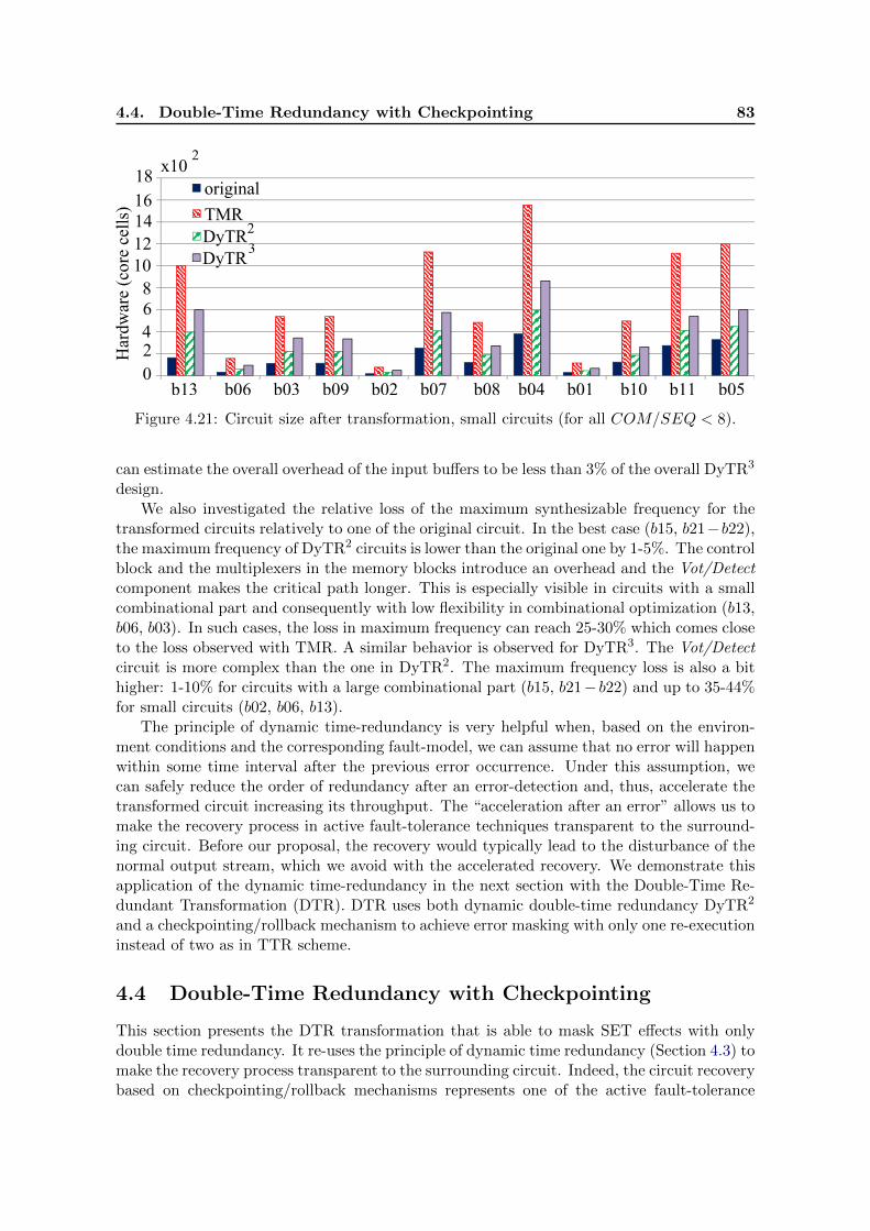
4.4. Double-Time Redundancy with Checkpointing 83
original
TMRDyTRDyTR
32
Har
dwar
e5(c
ore5
cells
)
b13555555b0655555b0355555b0955555b0255555b07555555b085555b0455555b01555555b1055555b1155555b055555
x102
02468
1012141618
5
Figure 4.21: Circuit size after transformation, small circuits (for all COM/SEQ < 8).
can estimate the overall overhead of the input buffers to be less than 3% of the overall DyTR3
design.We also investigated the relative loss of the maximum synthesizable frequency for the
transformed circuits relatively to one of the original circuit. In the best case (b15, b21−b22),the maximum frequency of DyTR2 circuits is lower than the original one by 1-5%. The controlblock and the multiplexers in the memory blocks introduce an overhead and the Vot/Detectcomponent makes the critical path longer. This is especially visible in circuits with a smallcombinational part and consequently with low flexibility in combinational optimization (b13,b06, b03). In such cases, the loss in maximum frequency can reach 25-30% which comes closeto the loss observed with TMR. A similar behavior is observed for DyTR3. The Vot/Detectcircuit is more complex than the one in DyTR2. The maximum frequency loss is also a bithigher: 1-10% for circuits with a large combinational part (b15, b21− b22) and up to 35-44%for small circuits (b02, b06, b13).
The principle of dynamic time-redundancy is very helpful when, based on the environ-ment conditions and the corresponding fault-model, we can assume that no error will happenwithin some time interval after the previous error occurrence. Under this assumption, wecan safely reduce the order of redundancy after an error-detection and, thus, accelerate thetransformed circuit increasing its throughput. The “acceleration after an error” allows us tomake the recovery process in active fault-tolerance techniques transparent to the surround-ing circuit. Before our proposal, the recovery would typically lead to the disturbance of thenormal output stream, which we avoid with the accelerated recovery. We demonstrate thisapplication of the dynamic time-redundancy in the next section with the Double-Time Re-dundant Transformation (DTR). DTR uses both dynamic double-time redundancy DyTR2
and a checkpointing/rollback mechanism to achieve error masking with only one re-executioninstead of two as in TTR scheme.
4.4 Double-Time Redundancy with Checkpointing
This section presents the DTR transformation that is able to mask SET effects with onlydouble time redundancy. It re-uses the principle of dynamic time redundancy (Section 4.3) tomake the recovery process transparent to the surrounding circuit. Indeed, the circuit recoverybased on checkpointing/rollback mechanisms represents one of the active fault-tolerance

84 Chapter 4. Time-Redundancy Circuit Transformations
techniques that are responsive to an error-detection event and adjust the circuit functionalityto recovery from errors. In particular, double-time redundancy allows us to detect an error,to rollback to a previous correct checkpointed state and to perform a third re-computation.Such reactions usually imply the disturbance of the normal output stream. However, aswe will show, the combination of the dynamic time-redundancy with a checkpoing/rollbackmechanism allows us to overcome this drawback and to make the recovery invisible forthe surrounding circuit. The novelty of DTR consists in switching-off the time-redundancy(like in DyTR2) to perform the recovery fast enough so that the normal output stream isnot disturbed and the next possible SET does not occur during this unprotected recovery“speed-up”.
We show that any circuit transformed according to our DTR technique is able to maskany SET of the fault model SET (1 , 10 ) i.e., “at most one SET within 10 clock cycles”.As any presented time-redundancy transformation presented in this dissertation, DTR is anautomatic logic-level fault-tolerance transformation that does not depend on the implemen-tation technology (e.g., FPGA or ASIC). It naturally supports stream-to-stream processing.
Section 4.4.1 presents the general principle of combining error-detection with recovery,and the use of input/output buffers. Each DTR subcomponent is explained in details inSections 4.4.2 to 4.4.5. Section 4.4.6 discusses DTR circuit functionality without an SEToccurrence and Section 4.4.7 explains the recovery process after an error detection. Section4.4.8 presents the informal proof that the transformed circuit is fault-tolerant for all possibleerrors according to the fault-model. The formal proof of DTR correctness in Coq is explainedin the next chapter. The hardware overheads and maximum throughput of the original,TMR, and DTR circuits are compared in Section 4.4.9.
4.4.1 Principle of Time Redundancy with Checkpointing
The main features of the DTR transformation are illustrated in Figure 4.22. The primaryinput stream is upsampled twice and given to the combinational part to detect errors bycomparison (written C). The line . . . , s1, s2, t1, t2, . . . represents paired internal statesand . . . , a, a, b, b, . . . paired bits in the output stream. In normal mode, checkpointing isperformed every other cycle. When an error is detected (e.g., t1 6= t′2), a recovery processconsisting of a rollback and a re-execution is triggered (resulting in the internal state t3).
s1 s2 t 1 t 2 w1 w2 ...C C
Output stream(both cases)
Executionwith SET
a a b b c c ... kd... ...
rollback
Speed up
no redundacy
Output buffer
k
s1 s2 t 1 t 2 w1 w2 ...C CExecution
without SETu1 u2 ...
CC
C
...
...Error
detected
t3u1'
Figure 4.22: Overview of the DTR transformation.
According to the fault-model SET (1 ,K ), no fault occurs within K clock cycles after thelast fault. This allows us to switch off time-redundancy during the recovery phase and to “ac-
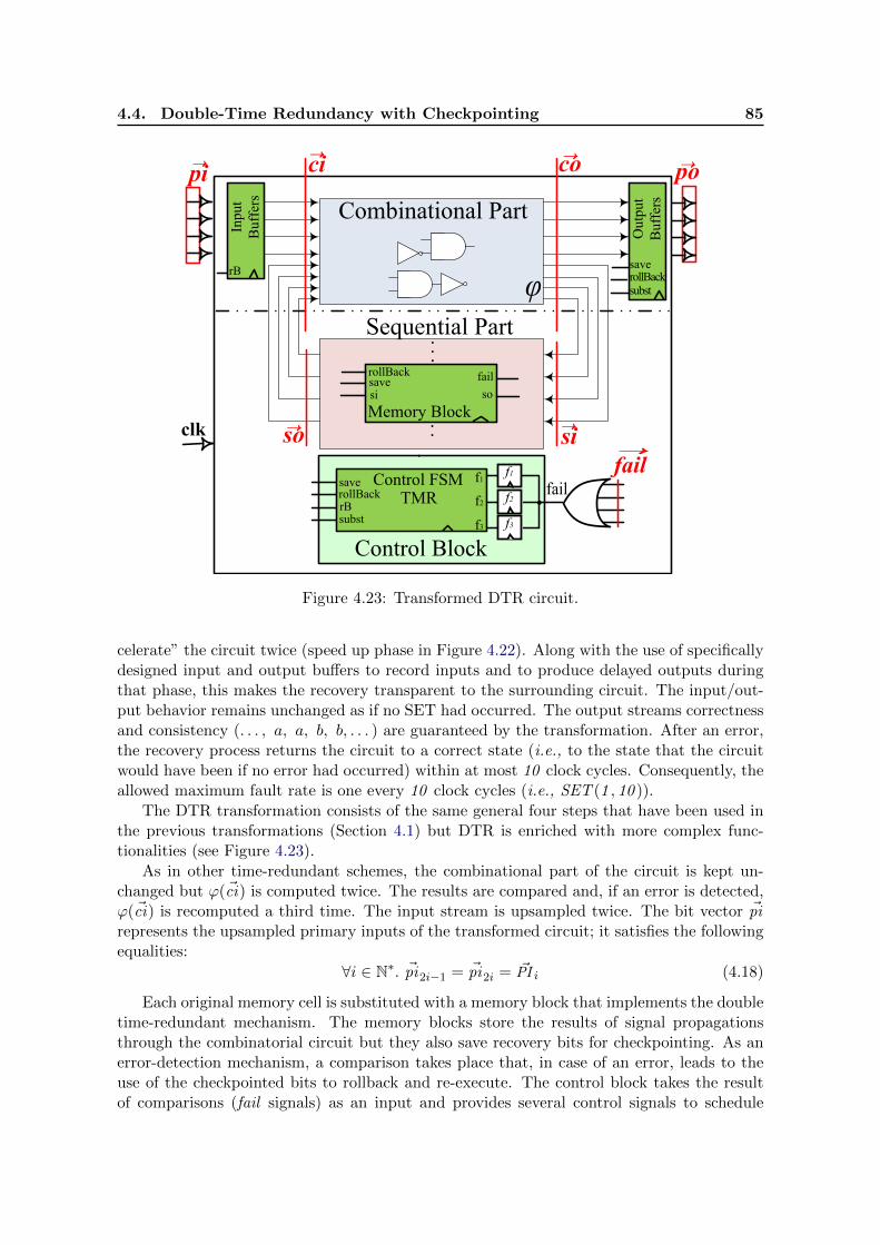
4.4. Double-Time Redundancy with Checkpointing 85
SequentialRPart
clk
CombinationalRPartR
ini:C2
MemoryRBlocksi so
failsaverollBack
Inpu
tRB
uffe
rsrB
Out
putR
Buf
fers
save
ci copi po
so si
rollBacksubstφ
ini:C2
f3
ControlRBlock
saverollBackrBsubst
failf1
f2
f1
TMR f2
f3
ControlRFSM
Figure 4.23: Transformed DTR circuit.
celerate” the circuit twice (speed up phase in Figure 4.22). Along with the use of specificallydesigned input and output buffers to record inputs and to produce delayed outputs duringthat phase, this makes the recovery transparent to the surrounding circuit. The input/out-put behavior remains unchanged as if no SET had occurred. The output streams correctnessand consistency (. . . , a, a, b, b, . . . ) are guaranteed by the transformation. After an error,the recovery process returns the circuit to a correct state (i.e., to the state that the circuitwould have been if no error had occurred) within at most 10 clock cycles. Consequently, theallowed maximum fault rate is one every 10 clock cycles (i.e., SET (1 , 10 )).
The DTR transformation consists of the same general four steps that have been used inthe previous transformations (Section 4.1) but DTR is enriched with more complex func-tionalities (see Figure 4.23).
As in other time-redundant schemes, the combinational part of the circuit is kept un-changed but ϕ(~ci) is computed twice. The results are compared and, if an error is detected,ϕ(~ci) is recomputed a third time. The input stream is upsampled twice. The bit vector ~pirepresents the upsampled primary inputs of the transformed circuit; it satisfies the followingequalities:
∀i ∈ N∗. ~pi2i−1 = ~pi2i = ~PI i (4.18)
Each original memory cell is substituted with a memory block that implements the doubletime-redundant mechanism. The memory blocks store the results of signal propagationsthrough the combinatorial circuit but they also save recovery bits for checkpointing. As anerror-detection mechanism, a comparison takes place that, in case of an error, leads to theuse of the checkpointed bits to rollback and re-execute. The control block takes the resultof comparisons (fail signals) as an input and provides several control signals to schedule
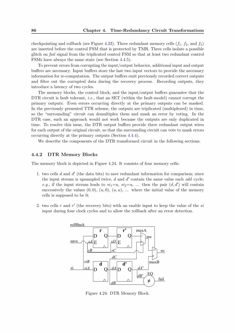
86 Chapter 4. Time-Redundancy Circuit Transformations
checkpointing and rollback (see Figure 4.23). Three redundant memory cells (f1, f2, and f3)are inserted before the control FSM that is protected by TMR. Three cells isolate a possibleglitch on fail signal from the triplicated control FSM so that at least two redundant controlFSMs have always the same state (see Section 4.4.5).
To prevent errors from corrupting the input/output behavior, additional input and outputbuffers are necessary. Input buffers store the last two input vectors to provide the necessaryinformation for re-computation. The output buffers emit previously recorded correct outputsand filter out the corrupted data during the recovery process. Recording outputs, theyintroduce a latency of two cycles.
The memory blocks, the control block, and the input/output buffers guarantee that theDTR circuit is fault tolerant, i.e., that an SET (within the fault-model) cannot corrupt theprimary outputs. Even errors occurring directly at the primary outputs can be masked.In the previously presented TTR scheme, the outputs are triplicated (multiplexed) in time,so the “surrounding” circuit can demultiplex them and mask an error by voting. In theDTR case, such an approach would not work because the outputs are only duplicated intime. To resolve this issue, the DTR output buffers provide three redundant output wiresfor each output of the original circuit, so that the surrounding circuit can vote to mask errorsoccurring directly at the primary outputs (Section 4.4.4).
We describe the components of the DTR transformed circuit in the following sections.
4.4.2 DTR Memory Blocks
The memory block is depicted in Figure 4.24. It consists of four memory cells:
1. two cells d and d′ (the data bits) to save redundant information for comparison; sincethe input stream is upsampled twice, d and d′ contain the same value each odd cycle;e.g., if the input stream leads to si1=u, si2=u, ... then the pair (d, d′) will containsuccessively the values (0, 0), (u, 0), (u, u), ... where the initial value of the memorycells is supposed to be 0;
2. two cells r and r′ (the recovery bits) with an enable input to keep the value of the siinput during four clock cycles and to allow the rollback after an error detection.
Qr
DE
Q Qr'
DE
Q
Qd
D Q Qd'
D Q
save 0
1
C
0
1C
si
so
rollBack
≠ fail
sA
sB
siA
siB
sC
sD
dA
dB
dC
dA'
dB'
mu
muxA
muxB
EQ
Figure 4.24: DTR Memory Block.

4.4. Double-Time Redundancy with Checkpointing 87
The DTR memory performs an error-detection comparison whose result is sent as a failsignal to the DTR control block. As noted above, the comparison of d and d′ is meaningfulonly during the odd cycles and so is the fail signal which is read only at those cycles.
In addition to the data input signal (si in Figure 4.24), each DTR memory block takesas inputs the special global control signals save and rollBack produced by the control blockand used to organize the circuit recovery after an error detection.
In Figure 4.24 we name all the internal wires that are connected to multiple gates (e.g., theoutput of d is connected to 3 gates, hence the 3 names dA, dB, and dC). This will be usefulin Section 4.4.8 to address all possible corruptions caused by an SET.
4.4.3 DTR Input Buffers
An input buffer is inserted at each primary input of the original circuit to keep the two lastbits of the input stream. The buffer is implemented as a pipeline of two memory cells, band b′, as shown in Figure 4.25. The signal rB is raised by the control block during therecovery process (Figure 4.27).
bD Q
1
0
C
cib'
D Q
pi
rB
Figure 4.25: DTR input buffer (pi primary input).
The cells b and b′ are used only during the recovery process in order to re-execute the lasttwo cycles. These bits are provided to the combinational part instead of the bits from theinput streams. They also serve to store the inputs that keep coming during those two cycles.During the recovery, the vector ~ci consists of (i) the first part ~pi coming from the inputbuffers and (ii) the second part ~so coming from the rollbacked memory blocks. If an error isdetected at cycle i, then the rollback is performed at cycle i+ 1 and the vector ~pi i−1⊕ ~soi−1
is provided to the combinational part (exactly the input vector already supplied 2 cyclesbefore).
From Eq. (4.18), we see that b and b′ represent two identical (resp. distinct) upsampledbits at each odd (resp. even) clock cycle: ~b2i−1 =~b′2i−1. Since error detection occurs at oddcycles, the recovery, which starts a cycle after, will read two different non-redundant inputsfrom ~b and ~b′. This is consistent with the speedup of the circuit during the recovery. Thebehavior of input buffers during the recovery is illustrated in Section 4.4.7.
4.4.4 DTR Output Buffers
The error recovery procedure disturbs the vector stream ~co in comparison with the normaloperating mode. To mask this effect at the primary outputs, we insert a DTR output buffer(Figure 4.26) before each primary output. They produce correct outputs but introduce, innormal mode, a latency loss of two clock cycles.
The output buffer is designed to be also fault-tolerant to any SET occurring inside or atits outputs. To achieve this property, the new primary outputs are triplicated (poA, poB ,poC ). The output buffers ensure that at least two out of them are correct at each even cycle.
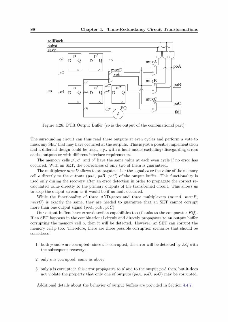
88 Chapter 4. Time-Redundancy Circuit Transformations
Qo
D Q Qo'
D Q0
1C
0
1C
co
poA
rollBack
≠ fail
cA
cB
oA
oB
oA'
oC'
muxA
muxB
Qo''
D Q
Qp
D Q Qp'
D Q
0
1C
subst
poB
poCmuxC
oB'
cC
0
1C
oC
save
muxDsub
EQ
Figure 4.26: DTR Output Buffer (co is the output of the combinational part).
The surrounding circuit can thus read these outputs at even cycles and perform a vote tomask any SET that may have occurred at the outputs. This is just a possible implementationand a different design could be used, e.g., with a fault-model excluding/disregarding errorsat the outputs or with different interface requirements.
The memory cells p′, o′, and o′′ have the same value at each even cycle if no error hasoccurred. With an SET, the correctness of only two of them is guaranteed.
The multiplexer muxD allows to propagate either the signal co or the value of the memorycell o directly to the outputs (poA, poB , poC ) of the output buffer. This functionality isused only during the recovery after an error detection in order to propagate the correct re-calculated value directly to the primary outputs of the transformed circuit. This allows usto keep the output stream as it would be if no fault occurred.
While the functionality of three AND-gates and three multiplexers (muxA, muxB,muxC) is exactly the same, they are needed to guarantee that an SET cannot corruptmore than one output signal (poA, poB , poC ).
Our output buffers have error-detection capabilities too (thanks to the comparator EQ).If an SET happens in the combinational circuit and directly propagates to an output buffercorrupting the memory cell o, then it will be detected. However, an SET can corrupt thememory cell p too. Therefore, there are three possible corruption scenarios that should beconsidered:
1. both p and o are corrupted: since o is corrupted, the error will be detected by EQ withthe subsequent recovery;
2. only o is corrupted: same as above;
3. only p is corrupted: this error propagates to p′ and to the output poA then, but it doesnot violate the property that only one of outputs (poA, poB , poC ) may be corrupted.
Additional details about the behavior of output buffers are provided in Section 4.4.7.
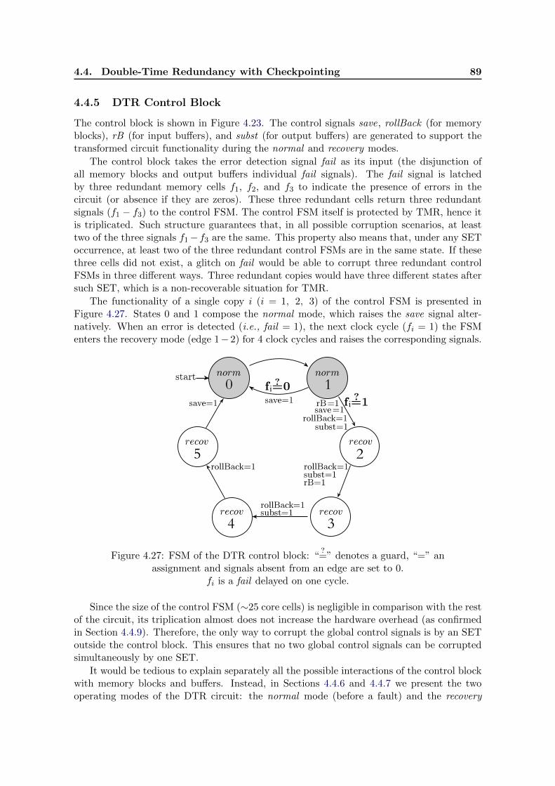
4.4. Double-Time Redundancy with Checkpointing 89
4.4.5 DTR Control Block
The control block is shown in Figure 4.23. The control signals save, rollBack (for memoryblocks), rB (for input buffers), and subst (for output buffers) are generated to support thetransformed circuit functionality during the normal and recovery modes.
The control block takes the error detection signal fail as its input (the disjunction ofall memory blocks and output buffers individual fail signals). The fail signal is latchedby three redundant memory cells f1, f2, and f3 to indicate the presence of errors in thecircuit (or absence if they are zeros). These three redundant cells return three redundantsignals (f1 − f3) to the control FSM. The control FSM itself is protected by TMR, hence itis triplicated. Such structure guarantees that, in all possible corruption scenarios, at leasttwo of the three signals f1−f3 are the same. This property also means that, under any SEToccurrence, at least two of the three redundant control FSMs are in the same state. If thesethree cells did not exist, a glitch on fail would be able to corrupt three redundant controlFSMs in three different ways. Three redundant copies would have three different states aftersuch SET, which is a non-recoverable situation for TMR.
The functionality of a single copy i (i = 1, 2, 3) of the control FSM is presented inFigure 4.27. States 0 and 1 compose the normal mode, which raises the save signal alter-natively. When an error is detected (i.e., fail = 1), the next clock cycle (fi = 1) the FSMenters the recovery mode (edge 1− 2) for 4 clock cycles and raises the corresponding signals.
i
i
0 1
2
34
5
Figure 4.27: FSM of the DTR control block: “?=” denotes a guard, “=” an
assignment and signals absent from an edge are set to 0.fi is a fail delayed on one cycle.
Since the size of the control FSM (∼25 core cells) is negligible in comparison with the restof the circuit, its triplication almost does not increase the hardware overhead (as confirmedin Section 4.4.9). Therefore, the only way to corrupt the global control signals is by an SEToutside the control block. This ensures that no two global control signals can be corruptedsimultaneously by one SET.
It would be tedious to explain separately all the possible interactions of the control blockwith memory blocks and buffers. Instead, in Sections 4.4.6 and 4.4.7 we present the twooperating modes of the DTR circuit: the normal mode (before a fault) and the recovery
90 Chapter 4. Time-Redundancy Circuit Transformations
mode (after a fault). Section 4.4.8, which examines all possible SETs, also clarifies themechanisms of the different components.
4.4.6 Normal Execution Mode
If no error is detected, the circuit is working in the normal operating mode. During thismode, the signal rollBack is always set to zero, while save is raised every even cycle:
save2i−1 = 0 and save2i = 1 (4.19)
Since save is the enable signal of memory cells r and r′, it organizes a four-cycle delay fromsi to r ′ in normal mode. The internal behavior of each DTR memory block in normal modecan be described by the following equations:
rollBacki = 0
~si i = ~di+1 = ~d′i+2 = ~soi+2
~si2i = ~r2i+1 = ~r2i+2 = ~r′2i+3 = ~r′2i+4
save2i−1 = 0, save2i = 1
(4.20)
It is easy to show that the DTR circuit verifies the same equalities as Eq. (4.1) for theoriginal circuit:
~coi = ϕ(~ci i) ~ci i = ~pi i ⊕ ~soi ~coi = ~poi ⊕ ~si i (4.21)
From Eqs. (4.18), (4.20), and (4.21), we can derive two properties for the normal operatingmode. First, the output bit stream ~co of the combinational part after the circuit transforma-tion is a double-time upsampling of the corresponding bit stream ~CO of the original circuit.Formally:
Property 4.3. ∀i ∈ N∗. ~co2i−1 = ~co2i = ~COi
Proof. We assume that the two cells d and d′ of each memory block are initialized as theoriginal cell, and therefore ~so1 = ~so2 = ~SO1. By Eqs. (4.1) and (4.21), we have ~co1 = ~co2 =~CO1. The proof is then a simple induction using Eqs. (4.1), (4.18), and (4.21).
Second, at each odd cycle, the outputs of the cells d and d′ are equal:
Property 4.4. ∀i ∈ N∗. ~d2i−1 = ~d′2i−1
Proof. At the first cycle (i=1), the property is true by the same initialization hypothesis asabove. Property 4.4 and Eq. (4.21) entail that ~si2i−1 = ~si2i. By Eq. (4.20), we have:
~si2i = ~d2i+1 = ~d′2i+2
‖~si2i−1 = ~d2i = ~d′2i+1
and thus, ∀i > 0, ~d2i+1 = ~d′2i+1, which is equivalent to ∀i > 1, ~d2i−1 = ~d′2i−1.
For error detection, we check the violation of Property 4.4 which is performed by the EQcomparator (Figure 4.24). If at some odd cycle 2j − 1 the d and d′ cells of a memory blockdiffer, an error is detected and the fail signal will be raised (fail2j−1 = 1). The circuit has to
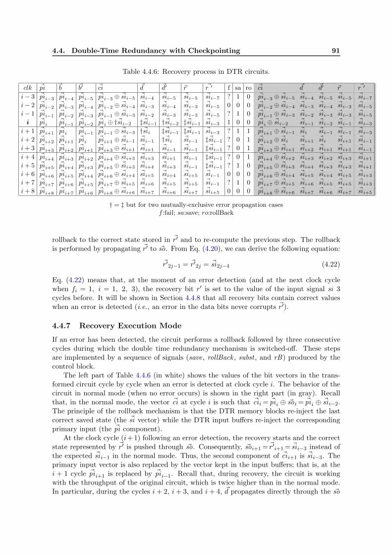
4.4. Double-Time Redundancy with Checkpointing 91
Table 4.4.6: Recovery process in DTR circuits.
clk ~pi ~b ~b′ ~ci ~d ~d′ ~r ~r ′ f sa ro ~ci ~d ~d′ ~r ~r ′
i− 3 ~pi i−3 ~pi i−4 ~pi i−5 ~pi i−3 ⊕ ~si i−5 ~si i−4 ~si i−5 ~si i−5 ~si i−7 ? 1 0 ~pi i−3 ⊕ ~si i−5 ~si i−4 ~si i−5 ~si i−5 ~si i−7i− 2 ~pi i−2 ~pi i−3 ~pi i−4 ~pi i−2 ⊕ ~si i−4 ~si i−3 ~si i−4 ~si i−3 ~si i−5 0 0 0 ~pi i−2 ⊕ ~si i−4 ~si i−3 ~si i−4 ~si i−3 ~si i−5i− 1 ~pi i−1 ~pi i−2 ~pi i−3 ~pi i−1 ⊕ ~si i−3 ~si i−2 ~si i−3 ~si i−3 ~si i−5 ? 1 0 ~pi i−1 ⊕ ~si i−3 ~si i−2 ~si i−3 ~si i−3 ~si i−5i ~pi i ~pi i−1 ~pi i−2 ~pi i ⊕ †~si i−2 ‡~si i−1 †~si i−2 ‡~si i−1 ~si i−3 1 0 0 ~pi i ⊕ ~si i−2 ~si i−1 ~si i−2 ~si i−1 ~si i−3
i+ 1 ~pi i+1~pi i ~pi i−1 ~pi i−1 ⊕ ~si i−3 †~si i ‡~si i−1 ‡~si i−1 ~si i−3 ? 1 1 ~pi i+1 ⊕ ~si i−1 ~si i ~si i−1 ~si i−1 ~si i−3
i+ 2 ~pi i+2~pi i+1
~pi i ~pi i+1 ⊕ ~si i−1 ~si i−1 †~si i ~si i−1 ‡~si i−1 ? 0 1 ~pi i+2 ⊕ ~si i ~si i+1~si i ~si i+1
~si i−1i+ 3 ~pi i+3
~pi i+2~pi i+1
~pi i+3 ⊕ ~si i+1~si i+1
~si i−1 ~si i−1 ‡~si i−1 ? 0 1 ~pi i+3 ⊕ ~si i+1~si i+2
~si i+1~si i+1
~si i−1i+ 4 ~pi i+4
~pi i+3~pi i+2
~pi i+4 ⊕ ~si i+3~si i+3
~si i+1~si i−1 ‡~si i−1 ? 0 1 ~pi i+4 ⊕ ~si i+2
~si i+3~si i+2
~si i+3~si i+1
i+ 5 ~pi i+5~pi i+4
~pi i+3~pi i+5 ⊕ ~si i+3
~si i+4~si i+3
~si i−1 ‡~si i−1 ? 1 0 ~pi i+5 ⊕ ~si i+3~si i+4
~si i+3~si i+3
~si i+1
i+ 6 ~pi i+6~pi i+5
~pi i+4~pi i+6 ⊕ ~si i+4
~si i+5~si i+4
~si i+5~si i−1 0 0 0 ~pi i+6 ⊕ ~si i+4
~si i+5~si i+4
~si i+5~si i+3
i+ 7 ~pi i+7~pi i+6
~pi i+5~pi i+7 ⊕ ~si i+5
~si i+6~si i+5
~si i+5~si i−1 ? 1 0 ~pi i+7 ⊕ ~si i+5
~si i+6~si i+5
~si i+5~si i+3
i+ 8 ~pi i+8~pi i+7
~pi i+6~pi i+8 ⊕ ~si i+6
~si i+7~si i+6
~si i+7~si i+5 0 0 0 ~pi i+8 ⊕ ~si i+6
~si i+7~si i+6
~si i+7~si i+5
† = ‡ but for two mutually-exclusive error propagation casesf :fail; sa:save; ro:rollBack
rollback to the correct state stored in ~r′ and to re-compute the previous step. The rollbackis performed by propagating ~r′ to ~so. From Eq. (4.20), we can derive the following equation:
~r′2j−1 = ~r′2j = ~si2j−4 (4.22)
Eq. (4.22) means that, at the moment of an error detection (and at the next clock cyclewhen fi = 1, i = 1, 2, 3), the recovery bit r′ is set to the value of the input signal si 3cycles before. It will be shown in Section 4.4.8 that all recovery bits contain correct valueswhen an error is detected (i.e., an error in the data bits never corrupts ~r′).
4.4.7 Recovery Execution Mode
If an error has been detected, the circuit performs a rollback followed by three consecutivecycles during which the double time redundancy mechanism is switched-off. These stepsare implemented by a sequence of signals (save, rollBack , subst , and rB) produced by thecontrol block.
The left part of Table 4.4.6 (in white) shows the values of the bit vectors in the trans-formed circuit cycle by cycle when an error is detected at clock cycle i. The behavior of thecircuit in normal mode (when no error occurs) is shown in the right part (in gray). Recallthat, in the normal mode, the vector ~ci at cycle i is such that ~ci i = ~pi i ⊕ ~soi = ~pi i ⊕ ~si i−2.The principle of the rollback mechanism is that the DTR memory blocks re-inject the lastcorrect saved state (the ~si vector) while the DTR input buffers re-inject the correspondingprimary input (the ~pi component).
At the clock cycle (i+ 1) following an error detection, the recovery starts and the correctstate represented by ~r′ is pushed through ~so. Consequently, ~soi+1 = ~r′i+1 = ~si i−3 instead ofthe expected ~si i−1 in the normal mode. Thus, the second component of ~ci i+1 is ~si i−3. Theprimary input vector is also replaced by the vector kept in the input buffers; that is, at thei + 1 cycle ~pi i+1 is replaced by ~pi i−1. Recall that, during recovery, the circuit is workingwith the throughput of the original circuit, which is twice higher than in the normal mode.In particular, during the cycles i+ 2, i+ 3, and i+ 4, ~d propagates directly through the ~so

92 Chapter 4. Time-Redundancy Circuit Transformations
outputs of each memory block, bypassing the memory cells ~d′. This is implemented by raisingrollBack and lowering save which control the muxA and muxB multiplexers appropriatelyin each memory block. This is safe since the SET (1 ,K ) fault-model guarantees that noadditional error can occur just after an SET.
Consider cycle i + 2: the second component of ~ci i+2 is ~si i−1 (~si i−2, which is identicalto ~si i−1, has been skipped). Similarly, the primary input vector is replaced by ~pi i+1, since,
in the input buffers, ~b′i+2 = ~pi i and ~pi i+1 = ~pi i. It follows that ~ci i+1 = ~pi i−1 ⊕ ~si i−3 and~ci i+2 = ~pi i+1 ⊕ ~si i−1.
Let us look more closely at how an error propagates and how it is masked. The error~di 6= ~d′i detected at cycle i does not indicate which of ~d or ~d′ is corrupted. The fault-modelonly guarantees that their simultaneous corruption is not possible. We consider both ofthem as potentially corrupted and the † and ‡ marks indicate the two possible bit vectorcorruptions. We track the error propagation cycle by cycle based on data dependenciesbetween vectors as shown in Table 4.4.6.
Case #1: If ~d′i contains a corrupted value †~si i−2, it contaminates ~ci i. Since this inputbit vector is corrupted, the outputs of the combinational circuit can be corrupted as wellsince ~di+1 that latches †~si i. This corrupted value propagates to ~d′, so ~d′i+2 = †~si i. Since~d′ is bypassed and ~d propagates directly through the wires ~so, the error at †~si i is logicallymasked at muxB by rollBack , which is raised during 4 cycles after the error detection.
Case #2: If ~di contains a corrupted value ‡~si i−1, it will propagate to ~d′ and ~d′i+1 =‡~si i−1.Since ‡~si i−1 has been latched by ~d and ~r at the same clock cycle, ~ri is also corrupted:~ri=‡~si i−1. When rollback happens at cycle i+ 1, ~r propagates to ~r′ and remains in ~r′ untilthe next raised save. The save signal is raised only 5 cycles after the error-detection, whenrollBack is lowered again. As a result, any error in ~r′i+5 will be re-written with a new correctdata and cannot propagate through signals ~so due to the logical masking by rollBack =0 atmuxB .
All corrupted signals disappear from the circuit state within 6 clock cycles after an errordetection. The whole circuit returns to a correct state within 8 cycles. As it is shown in thenext section, the error detection occurs at worst 2 cycles later after an SET.
Table 4.4.7 represents the behavior of output buffers in the same situation (i.e., therecovery procedure when an error is detected at cycle i). The signal names correspond toFigure 4.26 and Table 4.4.6.
The fail signal can be raised by any memory block as well as by any output buffer sincethe latter also have an error-detection mechanism (EQ comparator). Consequently, if anerror is detected at cycle i (fail = 1), we cannot assume the correctness of cells ~o and ~o′ inthe output buffers at this clock cycles (‡ ~coi−1, ‡ ~coi−2). Moreover, if a memory block signalsan error, the bit vector ~pi i ⊕ †~si i−2 coming from the memory blocks to the output bufferscan be corrupted too. However, in all corruption scenarios, the DTR circuit performs therollback at the next cycle i + 1 by re-calculating the bit vector ~coi−1 a third time. Theoutput buffers allow this recalculated correct bit-vector ~coi−1 to propagate directly to theprimary outputs ~poA/B/C through the multiplexers muxD − {muxA, muxB, muxC}. Insuch a way, the primary outputs of DTR circuits remain correct even one cycle after anerror-detection. The next even cycle, when fault-tolerance properties should be guaranteed,is the cycle i+ 3. If no error had occurred, the primary output values would have been equalto ~coi+1 = ~coi as the right part of Table 4.4.7 indicates (filled with grey color). To fulfillthis condition after an error occurrence, the outputs of cells ~o are propagated directly tothe primary outputs. As a result, the output buffers substitute twice the corrupted output
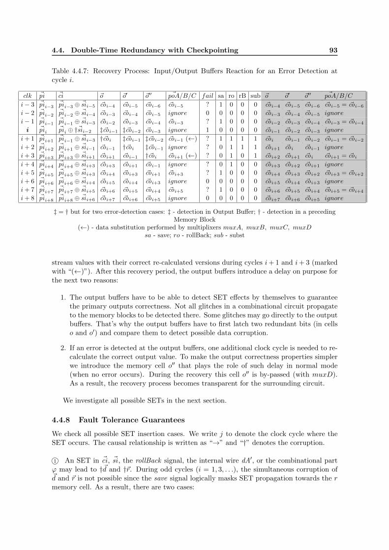
4.4. Double-Time Redundancy with Checkpointing 93
Table 4.4.7: Recovery Process: Input/Output Buffers Reaction for an Error Detection atcycle i.
clk ~pi ~ci ~o ~o′ ~o′′ ~poA/B/C fail sa ro rB sub ~o ~o′ ~o′′ ~poA/B/C
i− 3 ~pi i−3 ~pi i−3 ⊕ ~si i−5 ~coi−4 ~coi−5 ~coi−6 ~coi−5 ? 1 0 0 0 ~coi−4 ~coi−5 ~coi−6 ~coi−5 = ~coi−6i− 2 ~pi i−2 ~pi i−2 ⊕ ~si i−4 ~coi−3 ~coi−4 ~coi−5 ignore 0 0 0 0 0 ~coi−3 ~coi−4 ~coi−5 ignore
i− 1 ~pi i−1 ~pi i−1 ⊕ ~si i−3 ~coi−2 ~coi−3 ~coi−4 ~coi−3 ? 1 0 0 0 ~coi−2 ~coi−3 ~coi−4 ~coi−3 = ~coi−4i ~pi i ~pi i ⊕ †~si i−2 ‡ ~coi−1 ‡ ~coi−2 ~coi−3 ignore 1 0 0 0 0 ~coi−1 ~coi−2 ~coi−3 ignore
i+ 1 ~pi i+1~pi i−1 ⊕ ~si i−3 † ~coi ‡ ~coi−1 ‡ ~coi−2 ~coi−1 (←) ? 1 1 1 1 ~coi ~coi−1 ~coi−2 ~coi−1 = ~coi−2
i+ 2 ~pi i+2~pi i+1 ⊕ ~si i−1 ~coi−1 † ~coi ‡ ~coi−1 ignore ? 0 1 1 1 ~coi+1 ~coi ~coi−1 ignore
i+ 3 ~pi i+3~pi i+3 ⊕ ~si i+1 ~coi+1 ~coi−1 † ~coi ~coi+1 (←) ? 0 1 0 1 ~coi+2 ~coi+1 ~coi ~coi+1 = ~coi
i+ 4 ~pi i+4~pi i+4 ⊕ ~si i+3 ~coi+3 ~coi+1 ~coi−1 ignore ? 0 1 0 0 ~coi+3 ~coi+2 ~coi+1 ignore
i+ 5 ~pi i+5~pi i+5 ⊕ ~si i+3 ~coi+4 ~coi+3 ~coi+1 ~coi+3 ? 1 0 0 0 ~coi+4 ~coi+3 ~coi+2 ~coi+3 = ~coi+2
i+ 6 ~pi i+6~pi i+6 ⊕ ~si i+4 ~coi+5 ~coi+4 ~coi+3 ignore 0 0 0 0 0 ~coi+5 ~coi+4 ~coi+3 ignore
i+ 7 ~pi i+7~pi i+7 ⊕ ~si i+5 ~coi+6 ~coi+5 ~coi+4 ~coi+5 ? 1 0 0 0 ~coi+6 ~coi+5 ~coi+4 ~coi+5 = ~coi+4
i+ 8 ~pi i+8~pi i+8 ⊕ ~si i+6 ~coi+7 ~coi+6 ~coi+5 ignore 0 0 0 0 0 ~coi+7 ~coi+6 ~coi+5 ignore
‡ = † but for two error-detection cases: ‡ - detection in Output Buffer; † - detection in a precedingMemory Block
(←) - data substitution performed by multiplixers muxA, muxB, muxC, muxDsa - save; ro - rollBack; sub - subst
stream values with their correct re-calculated versions during cycles i+ 1 and i+ 3 (markedwith “(←)”). After this recovery period, the output buffers introduce a delay on purpose forthe next two reasons:
1. The output buffers have to be able to detect SET effects by themselves to guaranteethe primary outputs correctness. Not all glitches in a combinational circuit propagateto the memory blocks to be detected there. Some glitches may go directly to the outputbuffers. That’s why the output buffers have to first latch two redundant bits (in cellso and o′) and compare them to detect possible data corruption.
2. If an error is detected at the output buffers, one additional clock cycle is needed to re-calculate the correct output value. To make the output correctness properties simplerwe introduce the memory cell o′′ that plays the role of such delay in normal mode(when no error occurs). During the recovery this cell o′′ is by-passed (with muxD).As a result, the recovery process becomes transparent for the surrounding circuit.
We investigate all possible SETs in the next section.
4.4.8 Fault Tolerance Guarantees
We check all possible SET insertion cases. We write j to denote the clock cycle where theSET occurs. The causal relationship is written as “→” and “†” denotes the corruption.
1 An SET in ~ci , ~si , the rollBack signal, the internal wire dA′, or the combinational partϕ may lead to †~d and †~r. During odd cycles (i = 1, 3, . . .), the simultaneous corruption of~d and ~r is not possible since the save signal logically masks SET propagation towards the rmemory cell. As a result, there are two cases:
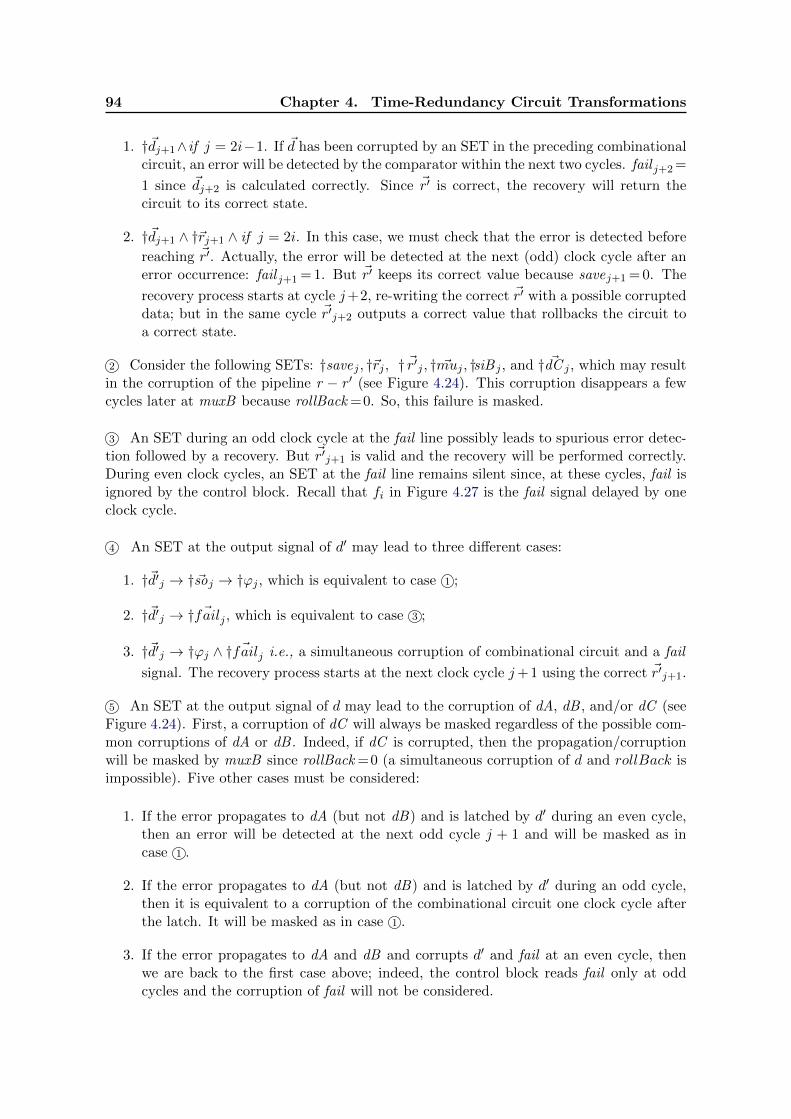
94 Chapter 4. Time-Redundancy Circuit Transformations
1. †~dj+1∧if j = 2i−1. If ~d has been corrupted by an SET in the preceding combinationalcircuit, an error will be detected by the comparator within the next two cycles. fail j+2 =
1 since ~dj+2 is calculated correctly. Since ~r′ is correct, the recovery will return thecircuit to its correct state.
2. †~dj+1 ∧ †~rj+1 ∧ if j = 2i. In this case, we must check that the error is detected before
reaching ~r′. Actually, the error will be detected at the next (odd) clock cycle after anerror occurrence: fail j+1 = 1. But ~r′ keeps its correct value because savej+1 = 0. The
recovery process starts at cycle j+2, re-writing the correct ~r′ with a possible corrupteddata; but in the same cycle ~r′j+2 outputs a correct value that rollbacks the circuit toa correct state.
2 Consider the following SETs: †savej , †~rj , † ~r′j , † ~muj , †siB j , and † ~dC j , which may resultin the corruption of the pipeline r − r ′ (see Figure 4.24). This corruption disappears a fewcycles later at muxB because rollBack =0. So, this failure is masked.
3 An SET during an odd clock cycle at the fail line possibly leads to spurious error detec-tion followed by a recovery. But ~r′j+1 is valid and the recovery will be performed correctly.During even clock cycles, an SET at the fail line remains silent since, at these cycles, fail isignored by the control block. Recall that fi in Figure 4.27 is the fail signal delayed by oneclock cycle.
4 An SET at the output signal of d′ may lead to three different cases:
1. †~d′j → † ~soj → †ϕj , which is equivalent to case 1 ;
2. †~d′j → † ~failj , which is equivalent to case 3 ;
3. †~d′j → †ϕj ∧ † ~failj i.e., a simultaneous corruption of combinational circuit and a fail
signal. The recovery process starts at the next clock cycle j+1 using the correct ~r′j+1.
5 An SET at the output signal of d may lead to the corruption of dA, dB , and/or dC (seeFigure 4.24). First, a corruption of dC will always be masked regardless of the possible com-mon corruptions of dA or dB . Indeed, if dC is corrupted, then the propagation/corruptionwill be masked by muxB since rollBack =0 (a simultaneous corruption of d and rollBack isimpossible). Five other cases must be considered:
1. If the error propagates to dA (but not dB) and is latched by d′ during an even cycle,then an error will be detected at the next odd cycle j + 1 and will be masked as incase 1 .
2. If the error propagates to dA (but not dB) and is latched by d′ during an odd cycle,then it is equivalent to a corruption of the combinational circuit one clock cycle afterthe latch. It will be masked as in case 1 .
3. If the error propagates to dA and dB and corrupts d′ and fail at an even cycle, thenwe are back to the first case above; indeed, the control block reads fail only at oddcycles and the corruption of fail will not be considered.
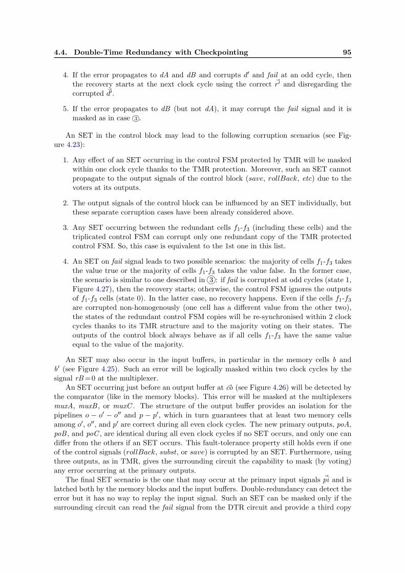
4.4. Double-Time Redundancy with Checkpointing 95
4. If the error propagates to dA and dB and corrupts d′ and fail at an odd cycle, thenthe recovery starts at the next clock cycle using the correct ~r′ and disregarding thecorrupted ~d′.
5. If the error propagates to dB (but not dA), it may corrupt the fail signal and it ismasked as in case 3 .
An SET in the control block may lead to the following corruption scenarios (see Fig-ure 4.23):
1. Any effect of an SET occurring in the control FSM protected by TMR will be maskedwithin one clock cycle thanks to the TMR protection. Moreover, such an SET cannotpropagate to the output signals of the control block (save, rollBack, etc) due to thevoters at its outputs.
2. The output signals of the control block can be influenced by an SET individually, butthese separate corruption cases have been already considered above.
3. Any SET occurring between the redundant cells f1-f3 (including these cells) and thetriplicated control FSM can corrupt only one redundant copy of the TMR protectedcontrol FSM. So, this case is equivalent to the 1st one in this list.
4. An SET on fail signal leads to two possible scenarios: the majority of cells f1-f3 takesthe value true or the majority of cells f1-f3 takes the value false. In the former case,the scenario is similar to one described in 3 : if fail is corrupted at odd cycles (state 1,Figure 4.27), then the recovery starts; otherwise, the control FSM ignores the outputsof f1-f3 cells (state 0). In the latter case, no recovery happens. Even if the cells f1-f3
are corrupted non-homogenously (one cell has a different value from the other two),the states of the redundant control FSM copies will be re-synchronised within 2 clockcycles thanks to its TMR structure and to the majority voting on their states. Theoutputs of the control block always behave as if all cells f1-f3 have the same valueequal to the value of the majority.
An SET may also occur in the input buffers, in particular in the memory cells b andb′ (see Figure 4.25). Such an error will be logically masked within two clock cycles by thesignal rB =0 at the multiplexer.
An SET occurring just before an output buffer at ~co (see Figure 4.26) will be detected bythe comparator (like in the memory blocks). This error will be masked at the multiplexersmuxA, muxB , or muxC . The structure of the output buffer provides an isolation for thepipelines o − o′ − o′′ and p − p′, which in turn guarantees that at least two memory cellsamong o′, o′′, and p′ are correct during all even clock cycles. The new primary outputs, poA,poB , and poC , are identical during all even clock cycles if no SET occurs, and only one candiffer from the others if an SET occurs. This fault-tolerance property still holds even if oneof the control signals (rollBack, subst, or save) is corrupted by an SET. Furthermore, usingthree outputs, as in TMR, gives the surrounding circuit the capability to mask (by voting)any error occurring at the primary outputs.
The final SET scenario is the one that may occur at the primary input signals ~pi and islatched both by the memory blocks and the input buffers. Double-redundancy can detect theerror but it has no way to replay the input signal. Such an SET can be masked only if thesurrounding circuit can read the fail signal from the DTR circuit and provide a third copy
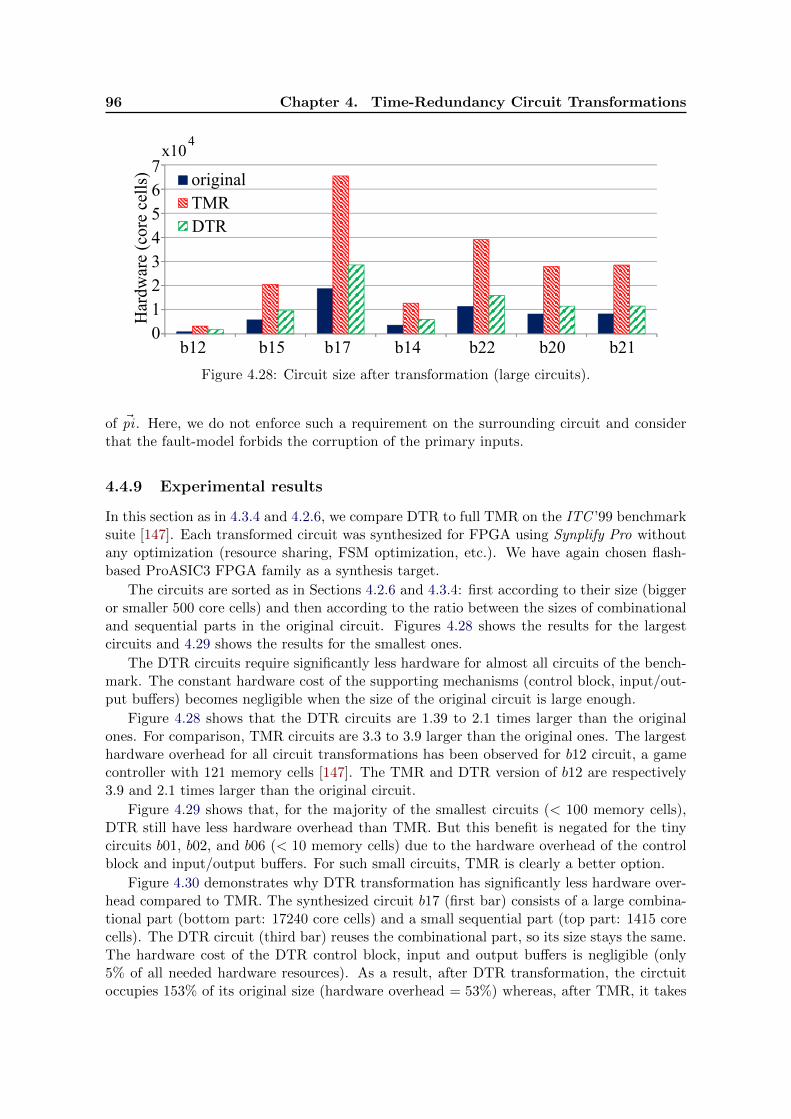
96 Chapter 4. Time-Redundancy Circuit Transformations
b12 b15 b17 b14 b22 b20 b21
76543210
Har
dwar
e (c
ore
cells
)
DTRTMRoriginal
x104
Figure 4.28: Circuit size after transformation (large circuits).
of ~pi . Here, we do not enforce such a requirement on the surrounding circuit and considerthat the fault-model forbids the corruption of the primary inputs.
4.4.9 Experimental results
In this section as in 4.3.4 and 4.2.6, we compare DTR to full TMR on the ITC ’99 benchmarksuite [147]. Each transformed circuit was synthesized for FPGA using Synplify Pro withoutany optimization (resource sharing, FSM optimization, etc.). We have again chosen flash-based ProASIC3 FPGA family as a synthesis target.
The circuits are sorted as in Sections 4.2.6 and 4.3.4: first according to their size (biggeror smaller 500 core cells) and then according to the ratio between the sizes of combinationaland sequential parts in the original circuit. Figures 4.28 shows the results for the largestcircuits and 4.29 shows the results for the smallest ones.
The DTR circuits require significantly less hardware for almost all circuits of the bench-mark. The constant hardware cost of the supporting mechanisms (control block, input/out-put buffers) becomes negligible when the size of the original circuit is large enough.
Figure 4.28 shows that the DTR circuits are 1.39 to 2.1 times larger than the originalones. For comparison, TMR circuits are 3.3 to 3.9 larger than the original ones. The largesthardware overhead for all circuit transformations has been observed for b12 circuit, a gamecontroller with 121 memory cells [147]. The TMR and DTR version of b12 are respectively3.9 and 2.1 times larger than the original circuit.
Figure 4.29 shows that, for the majority of the smallest circuits (< 100 memory cells),DTR still have less hardware overhead than TMR. But this benefit is negated for the tinycircuits b01, b02, and b06 (< 10 memory cells) due to the hardware overhead of the controlblock and input/output buffers. For such small circuits, TMR is clearly a better option.
Figure 4.30 demonstrates why DTR transformation has significantly less hardware over-head compared to TMR. The synthesized circuit b17 (first bar) consists of a large combina-tional part (bottom part: 17240 core cells) and a small sequential part (top part: 1415 corecells). The DTR circuit (third bar) reuses the combinational part, so its size stays the same.The hardware cost of the DTR control block, input and output buffers is negligible (only5% of all needed hardware resources). As a result, after DTR transformation, the circtuitoccupies 153% of its original size (hardware overhead = 53%) whereas, after TMR, it takes
4.4. Double-Time Redundancy with Checkpointing 97
DTRTMRoriginal
b13xxxxxb06 b03x xb09xxxb02x b07xx b08xxxb04xxx b01 b10xx b11x b05
181614121086420
Har
dwar
ex(c
orex
cells
)x10
2
Figure 4.29: Circuit size after transformation (small circuits).
sequentialcombin.
In./Out.buffers0Ctr.block
voters
Memoryblock
Har
dwar
eg3c
oreg
cells
2
original TMR DTR
7
6
5
4
3
2
1
0
x104
Figure 4.30: Transformed circuits profiling (for b17 ).
350% (harware overhead = 250%). The overhead of DTR is 4.7 times smaller than TMR forb17 and between 2.7 to 6.1 times smaller for the whole ITC ’99 benchmark suite.
Although DTR has a significantly smaller hardware overhead than TMR it decreases thecircuit throughput. Indeed, since the technique requires the input streams to be upsampled,the throughput of the transformed circuit is at least divided by two. Figure 4.31 shows theratio of the transformed circuit throughput w.r.t. the corresponding original throughput forthe ITC’99 benchmark suite (sorted left to right w.r.t. the size of the original circuit). Besidesthe upsampling, the DTR transformation influences by itself (as well as TMR) the circuitmaximum frequency, which also changes the final throughput. In particular, the maximumsynthesizable frequency after DTR transformation reaches ∼75% of the original frequencyfor small circuits (for TMR it is ∼77% ) and ∼92% for large circuits (for TMR it is ∼93%).
In the best case, the throughput of DTR circuits can reach 50% of the original circuitdue to the double upsampling of inputs. The control block and the multiplexers in memoryblocks also introduce a small extra overhead. For large circuits, the throughput is 40–50%of the original, while for small circuits it drops to 30–40%.
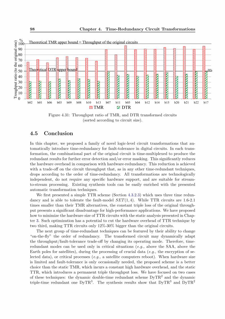
98 Chapter 4. Time-Redundancy Circuit Transformations
b02 b01 b06 b03 b09 b08 b10 b13 b07 b11 b05 b04 b12 b14 b15 b20 b21 b22 b17MM
Tro
ughp
utMr
atio
M(to
MtheM
orig
inal
Mone
)
TheoreticalMDTRMupperMboundM
TheoreticalMTMRMupperMboundM=MThroughputMofMtheMoriginalMcircuitsM1009080706050403020100
%
TMR DTR
50%
Figure 4.31: Throughput ratio of TMR, and DTR transformed circuits(sorted according to circuit size).
4.5 Conclusion
In this chapter, we proposed a family of novel logic-level circuit transformations that au-tomatically introduce time-redundancy for fault-tolerance in digital circuits. In each trans-formation, the combinational part of the original circuit is time-multiplexed to produce theredundant results for further error detection and/or error masking. This significantly reducesthe hardware overhead in comparison with hardware-redundancy. This reduction is achievedwith a trade-off on the circuit throughput that, as in any other time-redundant techniques,drops according to the order of time-redundancy. All transformations are technologicallyindependent, do not require any specific hardware support, and are suitable for stream-to-stream processing. Existing synthesis tools can be easily enriched with the presentedautomatic transformation techniques.
We first presented a simple TTR scheme (Section 4.3.2.3) which uses three time redun-dancy and is able to tolerate the fault-model SET (1, 4). While TTR circuits are 1.6-2.1times smaller than their TMR alternatives, the constant triple loss of the original through-put presents a significant disadvantage for high-performance applications. We have proposedhow to minimize the hardware size of TTR circuits with the static analysis presented in Chap-ter 3. Such optimization has a potential to cut the hardware overhead of TTR technique bytwo third, making TTR circuits only 12%-30% bigger than the original circuits.
The next group of time-redundant techniques can be featured by their ability to change“on-the-fly” the order of redundancy. The transformed circuit may dynamically adaptthe throughput/fault-tolerance trade-off by changing its operating mode. Therefore, time-redundant modes can be used only in critical situations (e.g., above the SAA, above theEarth poles for satellites), during the processing of crucial data (e.g., the encryption of se-lected data), or critical processes (e.g., a satellite computers reboot). When hardware sizeis limited and fault-tolerance is only occasionally needed, the proposed scheme is a betterchoice than the static TMR, which incurs a constant high hardware overhead, and the staticTTR, which introduces a permanent triple throughput loss. We have focused on two casesof these techniques: the dynamic double-time redundant scheme DyTR2 and the dynamictriple-time redundant one DyTR3. The synthesis results show that DyTR3 and DyTR2
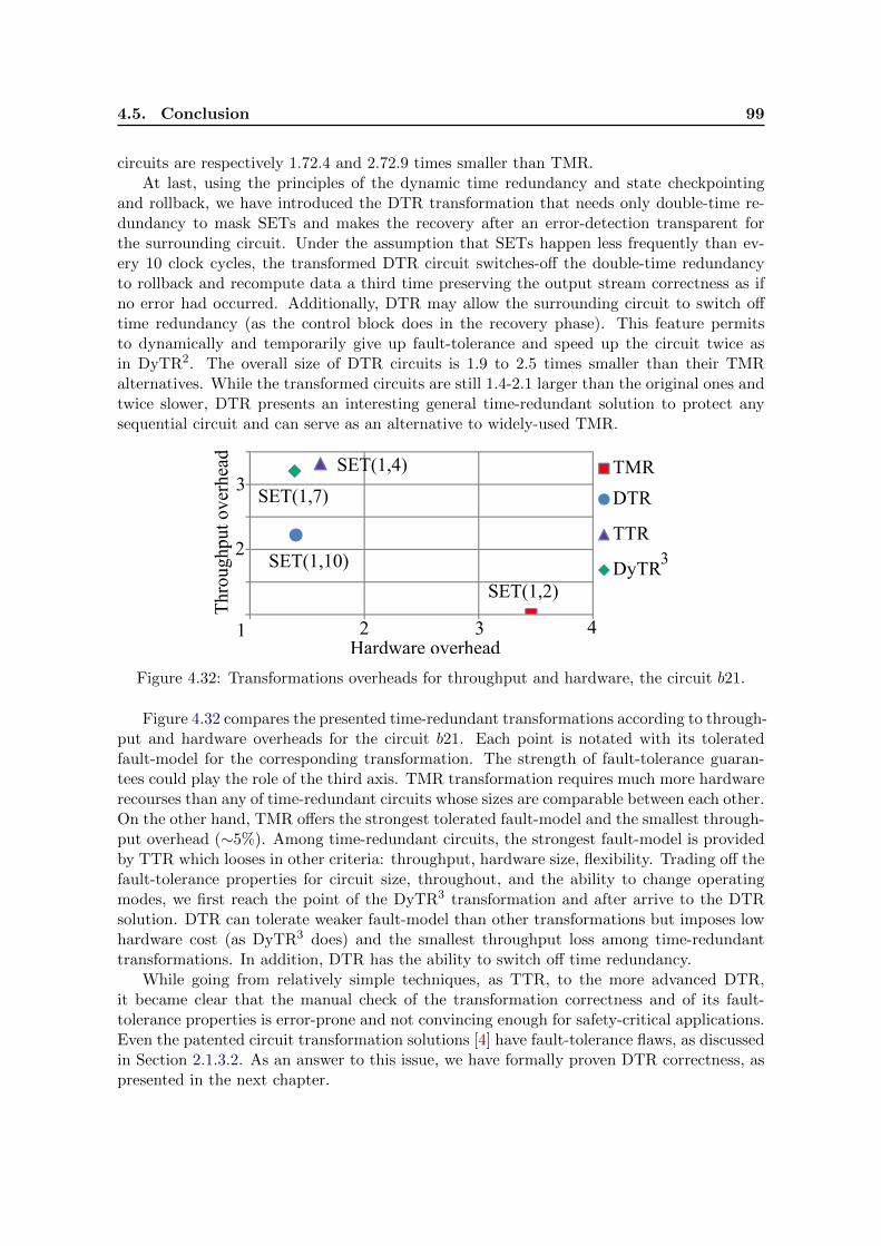
4.5. Conclusion 99
circuits are respectively 1.72.4 and 2.72.9 times smaller than TMR.At last, using the principles of the dynamic time redundancy and state checkpointing
and rollback, we have introduced the DTR transformation that needs only double-time re-dundancy to mask SETs and makes the recovery after an error-detection transparent forthe surrounding circuit. Under the assumption that SETs happen less frequently than ev-ery 10 clock cycles, the transformed DTR circuit switches-off the double-time redundancyto rollback and recompute data a third time preserving the output stream correctness as ifno error had occurred. Additionally, DTR may allow the surrounding circuit to switch offtime redundancy (as the control block does in the recovery phase). This feature permitsto dynamically and temporarily give up fault-tolerance and speed up the circuit twice asin DyTR2. The overall size of DTR circuits is 1.9 to 2.5 times smaller than their TMRalternatives. While the transformed circuits are still 1.4-2.1 larger than the original ones andtwice slower, DTR presents an interesting general time-redundant solution to protect anysequential circuit and can serve as an alternative to widely-used TMR.
TMR
DTR
TTR
DyTR
1
2
3SET(1,4)
SET(1,7)
SET(1,10)
SET(1,2)
2 3 4
3
Hardware overhead
Thr
ough
put o
verh
ead
Figure 4.32: Transformations overheads for throughput and hardware, the circuit b21.
Figure 4.32 compares the presented time-redundant transformations according to through-put and hardware overheads for the circuit b21. Each point is notated with its toleratedfault-model for the corresponding transformation. The strength of fault-tolerance guaran-tees could play the role of the third axis. TMR transformation requires much more hardwarerecourses than any of time-redundant circuits whose sizes are comparable between each other.On the other hand, TMR offers the strongest tolerated fault-model and the smallest through-put overhead (∼5%). Among time-redundant circuits, the strongest fault-model is providedby TTR which looses in other criteria: throughput, hardware size, flexibility. Trading off thefault-tolerance properties for circuit size, throughout, and the ability to change operatingmodes, we first reach the point of the DyTR3 transformation and after arrive to the DTRsolution. DTR can tolerate weaker fault-model than other transformations but imposes lowhardware cost (as DyTR3 does) and the smallest throughput loss among time-redundanttransformations. In addition, DTR has the ability to switch off time redundancy.
While going from relatively simple techniques, as TTR, to the more advanced DTR,it became clear that the manual check of the transformation correctness and of its fault-tolerance properties is error-prone and not convincing enough for safety-critical applications.Even the patented circuit transformation solutions [4] have fault-tolerance flaws, as discussedin Section 2.1.3.2. As an answer to this issue, we have formally proven DTR correctness, aspresented in the next chapter.

Chapter 5
Formal proof of the DTRTransformation
Since fault-tolerance is typically used in critical domains (aerospace, defence, etc), the cor-rectness of circuit transformations for fault-tolerance is essential. Along with functionalverification, the fault-tolerance properties have also to be checked. As we saw in Chapter 4,fault-tolerance techniques, like DTR, are often too complex to assure their correctness withmanual checks. Widely-used post-synthesis verification tools (e.g., model checking) are sim-ply inappropriate to prove that a transformation ensures fault-tolerance properties for allpossible circuits; only proof-based approaches are suitable.
In this chapter, we present a language-based solution to certify fault-tolerance techniquesfor digital circuits. Circuits are expressed in a gate-level HDL, fault-tolerance techniquesare described as automatic circuit transformations in that language, and fault-models arespecified as particular semantics of the HDL. These elements are formalized in the Coq proofassistant [155] and the properties, ensuring that for all circuits their transformed versionmasks all faults of the considered fault-model, can be expressed and proved. Proofs relymainly on relating the execution of the source circuit without faults to the execution of thetransformed circuit w.r.t. the considered fault-model. They make use of several techniques(case analysis, induction on the type or the structure of circuits, co-induction on inputstreams).
While our approach is general, our primary motivation is to certify the DTR techniquethat we have presented in Section 4.4. The DTR transformation combines double-time re-dundancy, micro-checkpointing, rollback, several execution modes, and input/output buffers.While we have manually shown its correctness (Section 4.4.8), DTR intricacy asks for a for-mal certification to make sure that no single-point of failure existed.
Section 5.1 introduces the syntax and semantics of our gate-level HDL. In Section 5.2,we present the specification of fault-models in the language formal semantics. Section 2explains the proof methodology adopted to show the correctness of circuit transformations.It is illustrated by examples taken from the simplest transformation: TMR. Section 5.4 in-troduces the DTR circuit transformation [20] and sketches the associated proofs. Section 5.5summarizes our contributions.
We use standard mathematical and semantic notations. The corresponding Coq specifi-cations and proofs are available online [156].
5.1 Circuit Description Language
We describe circuits at the gate level using a purely functional language inspired fromSheeran’s combinator-based languages such as µFP [157] or Ruby [158]. We equip our lan-guage with dependent types which, along with the language syntax, ensure that circuits arewell-formed by construction (gates correctly plugged, no dangling wires, no combinationalloops, . . . ).

102 Chapter 5. Formal proof of the DTR Transformation
Contrary to µFP or Ruby, our primary goal is not to make the description of circuitseasy but to keep the language as simple and minimal as possible to facilitate formal proofs.Our language contains only 3 logical gates, 5 plugs and 3 combining forms. It is best seen asa low-level core language used as the object code of a synthesis tool. We denote it as lddlfor Low-level Dependent Description Language.
5.1.1 Syntax of lddl
A bus of signals is described by the following type
B := ω | (B1 ∗B2)
A bus is either a single wire (ω) or a pair of buses (B1 ∗ B2). In other terms, signals aredefined as nested tuples. The constructors of lddl annotated with their types are gatheredin Figure 5.1. A circuit takes as parameters its input and output types and is either a logicgate, a plug, or composition of circuits.
Gates
not : Gate ω ω and,or : Gate (ω ∗ ω) ω
Plugs
id : ∀α,Plug α αfork : ∀α,Plug α (α ∗ α)swap : ∀α β,Plug (α ∗ β) (β ∗ α)lsh : ∀α β γ,Plug ((α ∗ β) ∗ γ) (α ∗ (β ∗ γ))rsh : ∀α β γ,Plug (α ∗ (β ∗ γ)) ((α ∗ β) ∗ γ)
Circuits
C ::= Gates| Plugs| C1 -◦-C2 : ∀α β γ,Circ α β → Circ β γ
→ Circ α γ| []C1, C2[] : ∀α β γ δ,Circ α γ → Circ β δ
→ Circ (α ∗ β) (γ ∗ δ)| x−C : ∀α β, bool→ Circ (α ∗ ω) (β ∗ ω)
→ Circ α β
Figure 5.1: lddl syntax.
The sets of logical gates and plugs are minimal but expressive enough to specify anycombinational circuit. Actually, extending those sets would have a marginal impact on theproofs.
The type of and and or, Gate (ω ∗ω) ω, indicates that they are gates taking a bus madeof two wires and returning one wire. Likewise, not has type Gate ω ω. Plugs, used to express(re)wiring, are polymorphic functions that duplicate or reorder buses: id leaves its input busunchanged, fork duplicates its input bus, swap inverts the order of its two input buses, lshand rsh reorder their three input buses.
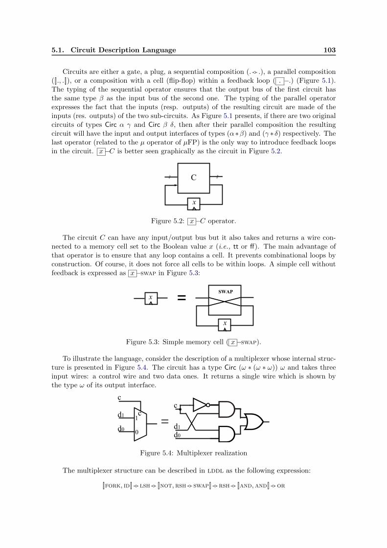
5.1. Circuit Description Language 103
Circuits are either a gate, a plug, a sequential composition (. -◦- .), a parallel composition([]., .[]), or a composition with a cell (flip-flop) within a feedback loop ( . −.) (Figure 5.1).The typing of the sequential operator ensures that the output bus of the first circuit hasthe same type β as the input bus of the second one. The typing of the parallel operatorexpresses the fact that the inputs (resp. outputs) of the resulting circuit are made of theinputs (res. outputs) of the two sub-circuits. As Figure 5.1 presents, if there are two originalcircuits of types Circ α γ and Circ β δ, then after their parallel composition the resultingcircuit will have the input and output interfaces of types (α∗β) and (γ ∗δ) respectively. Thelast operator (related to the µ operator of µFP) is the only way to introduce feedback loopsin the circuit. x−C is better seen graphically as the circuit in Figure 5.2.
C
x
Figure 5.2: x−C operator.
The circuit C can have any input/output bus but it also takes and returns a wire con-nected to a memory cell set to the Boolean value x (i.e., tt or ff). The main advantage ofthat operator is to ensure that any loop contains a cell. It prevents combinational loops byconstruction. Of course, it does not force all cells to be within loops. A simple cell withoutfeedback is expressed as x−swap in Figure 5.3:
SWAP
=x
x
Figure 5.3: Simple memory cell ( x−swap).
To illustrate the language, consider the description of a multiplexer whose internal struc-ture is presented in Figure 5.4. The circuit has a type Circ (ω ∗ (ω ∗ ω)) ω and takes threeinput wires: a control wire and two data ones. It returns a single wire which is shown bythe type ω of its output interface.
0
1c
c
d1
d0 d1d0
c
Figure 5.4: Multiplexer realization
The multiplexer structure can be described in lddl as the following expression:
[]fork, id[] -◦- lsh -◦- []not, rsh -◦- swap[] -◦-rsh -◦- []and,and[] -◦-or
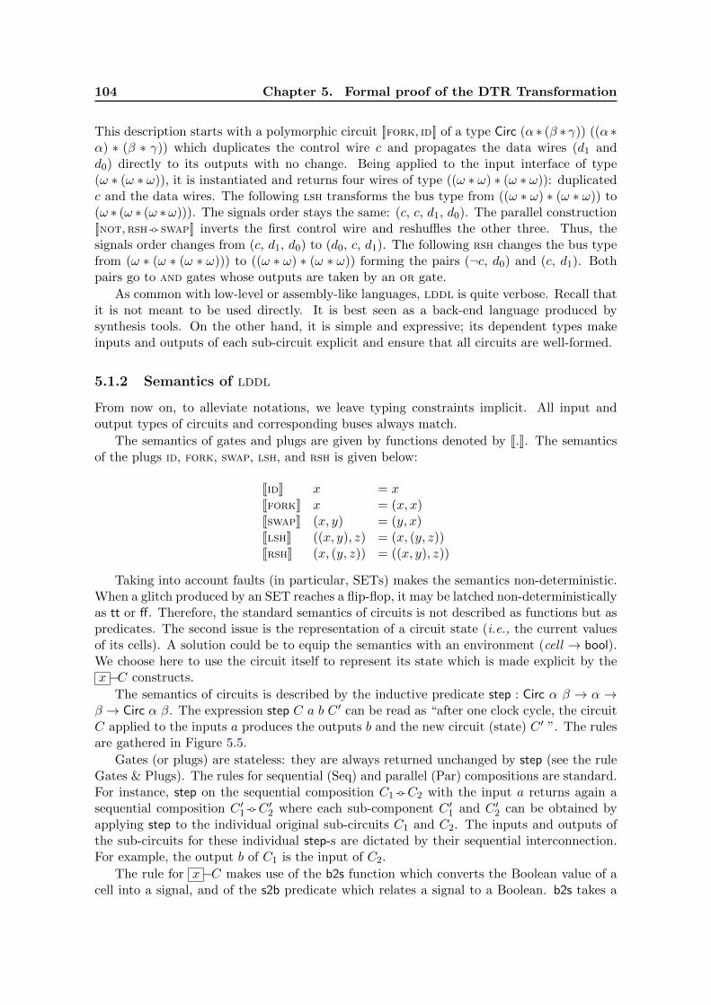
104 Chapter 5. Formal proof of the DTR Transformation
This description starts with a polymorphic circuit []fork, id[] of a type Circ (α ∗ (β ∗ γ)) ((α ∗α) ∗ (β ∗ γ)) which duplicates the control wire c and propagates the data wires (d1 andd0) directly to its outputs with no change. Being applied to the input interface of type(ω ∗ (ω ∗ ω)), it is instantiated and returns four wires of type ((ω ∗ ω) ∗ (ω ∗ ω)): duplicatedc and the data wires. The following lsh transforms the bus type from ((ω ∗ ω) ∗ (ω ∗ ω)) to(ω ∗ (ω ∗ (ω ∗ω))). The signals order stays the same: (c, c, d1, d0). The parallel construction[]not, rsh -◦- swap[] inverts the first control wire and reshuffles the other three. Thus, thesignals order changes from (c, d1, d0) to (d0, c, d1). The following rsh changes the bus typefrom (ω ∗ (ω ∗ (ω ∗ ω))) to ((ω ∗ ω) ∗ (ω ∗ ω)) forming the pairs (¬c, d0) and (c, d1). Bothpairs go to and gates whose outputs are taken by an or gate.
As common with low-level or assembly-like languages, lddl is quite verbose. Recall thatit is not meant to be used directly. It is best seen as a back-end language produced bysynthesis tools. On the other hand, it is simple and expressive; its dependent types makeinputs and outputs of each sub-circuit explicit and ensure that all circuits are well-formed.
5.1.2 Semantics of lddl
From now on, to alleviate notations, we leave typing constraints implicit. All input andoutput types of circuits and corresponding buses always match.
The semantics of gates and plugs are given by functions denoted by J.K. The semanticsof the plugs id, fork, swap, lsh, and rsh is given below:
JidK x = xJforkK x = (x, x)JswapK (x, y) = (y, x)JlshK ((x, y), z) = (x, (y, z))JrshK (x, (y, z)) = ((x, y), z))
Taking into account faults (in particular, SETs) makes the semantics non-deterministic.When a glitch produced by an SET reaches a flip-flop, it may be latched non-deterministicallyas tt or ff. Therefore, the standard semantics of circuits is not described as functions but aspredicates. The second issue is the representation of a circuit state (i.e., the current valuesof its cells). A solution could be to equip the semantics with an environment (cell → bool).We choose here to use the circuit itself to represent its state which is made explicit by thex−C constructs.
The semantics of circuits is described by the inductive predicate step : Circ α β → α →β → Circ α β. The expression step C a b C ′ can be read as “after one clock cycle, the circuitC applied to the inputs a produces the outputs b and the new circuit (state) C ′ ”. The rulesare gathered in Figure 5.5.
Gates (or plugs) are stateless: they are always returned unchanged by step (see the ruleGates & Plugs). The rules for sequential (Seq) and parallel (Par) compositions are standard.For instance, step on the sequential composition C1 -◦-C2 with the input a returns again asequential composition C ′1 -◦-C ′2 where each sub-component C ′1 and C ′2 can be obtained byapplying step to the individual original sub-circuits C1 and C2. The inputs and outputs ofthe sub-circuits for these individual step-s are dictated by their sequential interconnection.For example, the output b of C1 is the input of C2.
The rule for x−C makes use of the b2s function which converts the Boolean value of acell into a signal, and of the s2b predicate which relates a signal to a Boolean. b2s takes a
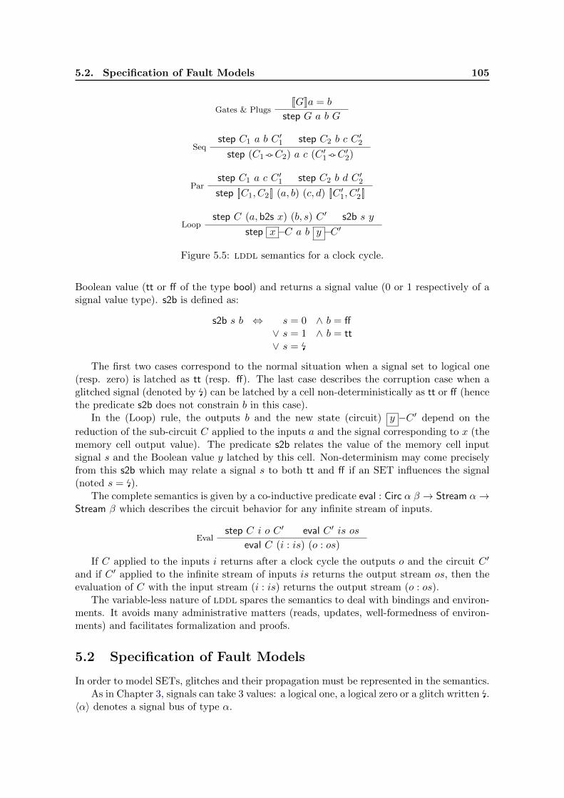
5.2. Specification of Fault Models 105
Gates & PlugsJGKa = b
step G a b G
Seqstep C1 a b C
′1 step C2 b c C
′2
step (C1 -◦-C2) a c (C ′1 -◦-C ′2)
Parstep C1 a c C
′1 step C2 b d C
′2
step []C1, C2[] (a, b) (c, d) []C ′1, C′2[]
Loopstep C (a, b2s x) (b, s) C ′ s2b s y
step x−C a b y −C ′
Figure 5.5: lddl semantics for a clock cycle.
Boolean value (tt or ff of the type bool) and returns a signal value (0 or 1 respectively of asignal value type). s2b is defined as:
s2b s b ⇔ s = 0 ∧ b = ff∨ s = 1 ∧ b = tt∨ s = �
The first two cases correspond to the normal situation when a signal set to logical one(resp. zero) is latched as tt (resp. ff). The last case describes the corruption case when aglitched signal (denoted by �) can be latched by a cell non-deterministically as tt or ff (hencethe predicate s2b does not constrain b in this case).
In the (Loop) rule, the outputs b and the new state (circuit) y −C ′ depend on the
reduction of the sub-circuit C applied to the inputs a and the signal corresponding to x (thememory cell output value). The predicate s2b relates the value of the memory cell inputsignal s and the Boolean value y latched by this cell. Non-determinism may come preciselyfrom this s2b which may relate a signal s to both tt and ff if an SET influences the signal(noted s = �).
The complete semantics is given by a co-inductive predicate eval : Circ α β → Stream α→Stream β which describes the circuit behavior for any infinite stream of inputs.
Evalstep C i o C ′ eval C ′ is os
eval C (i : is) (o : os)
If C applied to the inputs i returns after a clock cycle the outputs o and the circuit C ′
and if C ′ applied to the infinite stream of inputs is returns the output stream os, then theevaluation of C with the input stream (i : is) returns the output stream (o : os).
The variable-less nature of lddl spares the semantics to deal with bindings and environ-ments. It avoids many administrative matters (reads, updates, well-formedness of environ-ments) and facilitates formalization and proofs.
5.2 Specification of Fault Models
In order to model SETs, glitches and their propagation must be represented in the semantics.As in Chapter 3, signals can take 3 values: a logical one, a logical zero or a glitch written �.
〈α〉 denotes a signal bus of type α.
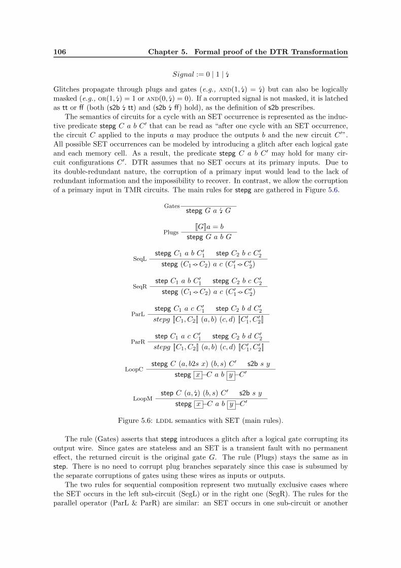
106 Chapter 5. Formal proof of the DTR Transformation
Signal := 0 | 1 | �
Glitches propagate through plugs and gates (e.g., and(1, �) = �) but can also be logicallymasked (e.g., or(1, �) = 1 or and(0, �) = 0). If a corrupted signal is not masked, it is latchedas tt or ff (both (s2b � tt) and (s2b � ff) hold), as the definition of s2b prescribes.
The semantics of circuits for a cycle with an SET occurrence is represented as the induc-tive predicate stepg C a b C ′ that can be read as “after one cycle with an SET occurrence,the circuit C applied to the inputs a may produce the outputs b and the new circuit C ′”.All possible SET occurrences can be modeled by introducing a glitch after each logical gateand each memory cell. As a result, the predicate stepg C a b C ′ may hold for many cir-cuit configurations C ′. DTR assumes that no SET occurs at its primary inputs. Due toits double-redundant nature, the corruption of a primary input would lead to the lack ofredundant information and the impossibility to recover. In contrast, we allow the corruptionof a primary input in TMR circuits. The main rules for stepg are gathered in Figure 5.6.
Gatesstepg G a � G
PlugsJGKa = b
stepg G a b G
SeqLstepg C1 a b C
′1 step C2 b c C
′2
stepg (C1 -◦-C2) a c (C ′1 -◦-C ′2)
SeqRstep C1 a b C
′1 stepg C2 b c C
′2
stepg (C1 -◦-C2) a c (C ′1 -◦-C ′2)
ParLstepg C1 a c C
′1 step C2 b d C
′2
stepg []C1, C2[] (a, b) (c, d) []C ′1, C′2[]
ParRstep C1 a c C
′1 stepg C2 b d C
′2
stepg []C1, C2[] (a, b) (c, d) []C ′1, C′2[]
LoopCstepg C (a, b2s x) (b, s) C ′ s2b s y
stepg x−C a b y −C ′
LoopMstep C (a, �) (b, s) C ′ s2b s y
stepg x−C a b y −C ′
Figure 5.6: lddl semantics with SET (main rules).
The rule (Gates) asserts that stepg introduces a glitch after a logical gate corrupting itsoutput wire. Since gates are stateless and an SET is a transient fault with no permanenteffect, the returned circuit is the original gate G. The rule (Plugs) stays the same as instep. There is no need to corrupt plug branches separately since this case is subsumed bythe separate corruptions of gates using these wires as inputs or outputs.
The two rules for sequential composition represent two mutually exclusive cases wherethe SET occurs in the left sub-circuit (SegL) or in the right one (SegR). The rules for theparallel operator (ParL & ParR) are similar: an SET occurs in one sub-circuit or another
5.3. Overview of Correctness Proofs 107
but not in both.
The rule (LoopC) represents the case where an SET occurs inside the sub-circuit C ofx−C structure. The rule (LoopM) represents the case where an SET occurs at the output
of the memory cell x which is taken as an input by C.
To summarize, stepg introduces non-deterministically a single glitch after a memory cellor a logical gate. Hence, if a circuit has n gates and m cells, it specifies n + m possibleexecutions, one execution per SET injection scenario.
Finally, the fault-model SET (1 ,K ) is expressed by the predicate setk eval : Nat →Circ α β → Stream α→ Stream β:
SetNstep C i o C ′ setk eval (pred n) C ′ is os
setk eval n C (i : is) (o : os)
SetGstepg C i o C ′ setk eval (pred K) C ′ is os
setk eval 0 C (i : is) (o : os)
The first argument of type Nat plays the role of a clock counter. The operator predreturns the previous natural number of its argument. A glitch can be introduced (by stepg)only if the counter is 0, as it is shown in the rule (SetG). When a glitch is introduced, thecounter is reset to enforce at least K − 1 normal execution cycles with step (rule (SetN)).When the counter is back to 0, both rules can be non-deterministically applied (note thatpred 0 = 0 in the rule (SetN) when n = 0).
5.3 Overview of Correctness Proofs
We illustrate the main steps of the correctness proof using examples taken from the simpleTMR transformation. The formal proof of DTR, which is based on similar principles, willbe presented in details in Section 5.4.
5.3.1 Transformation
TMR and the proposed fault-tolerance techniques can be specified by a program transfor-mation on the syntax of lddl. They are defined by induction of the syntax and replacementof each memory cell by a memory block (a small circuit). The TMR transformation takesa circuit of type Circ α β and returns a circuit of type Circ ((α ∗ α) ∗ α) ((β ∗ β) ∗ β). In-puts/outputs are triplicated to play the role of the inputs/outputs of each copy. The TMRcircuit transformation can be expressed as:
tmr(X) = [][]X,X[], X[] with X a gate/plugtmr(C1 -◦-C2) = tmr(C1) -◦-tmr(C2)tmr([]C1, C2[]) = s1 -◦- []tmr(C1),tmr(C2)[] -◦- s2
tmr( x−C) = x− x− x−(vot -◦-tmr(C) -◦- s3)
where s1, s2, s3 are plugs that re-shuffle wires. The first rule for gates and plugs triplicatesthem organizing three redundant copies in parallel. If the circuit is composed of two sub-circuits C1 and C2 connected sequentially, TMR is applied to each subcircuit. Since theirinterfaces are triplicated in the same manner, the interface compatibility is kept and thetriplicated circuits (tmr(C1), tmr(C2)) can be sequentially plugged.
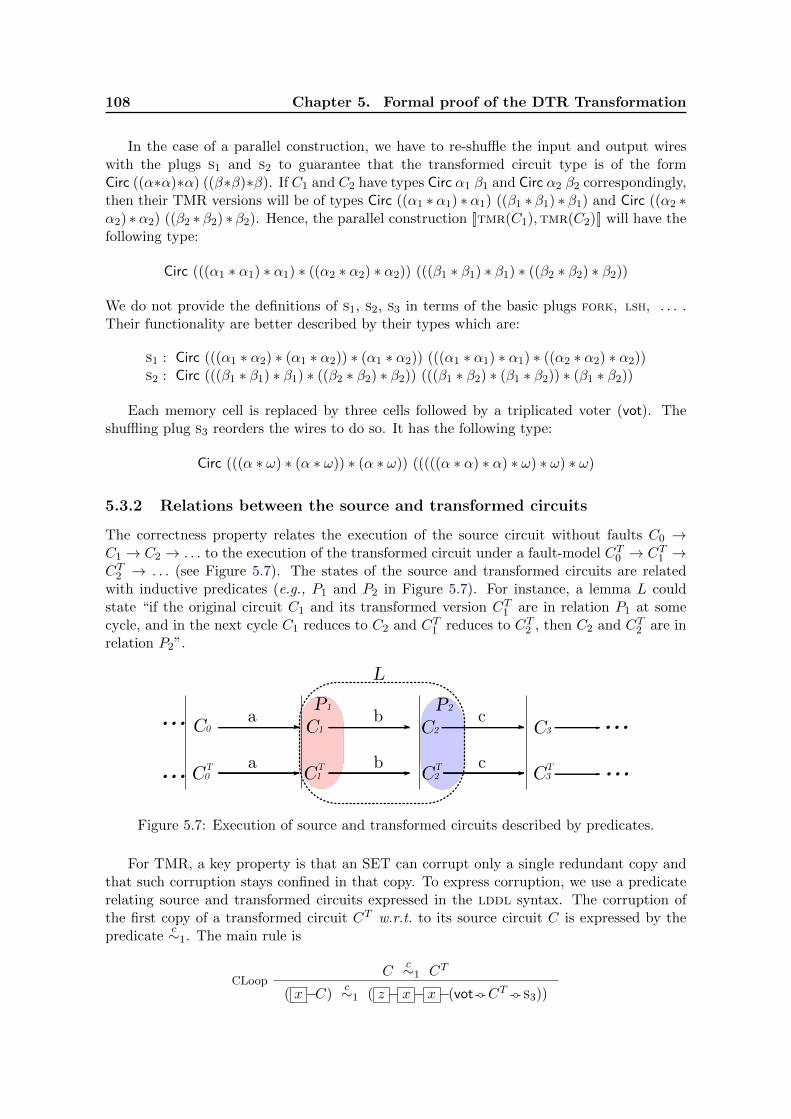
108 Chapter 5. Formal proof of the DTR Transformation
In the case of a parallel construction, we have to re-shuffle the input and output wireswith the plugs s1 and s2 to guarantee that the transformed circuit type is of the formCirc ((α∗α)∗α) ((β∗β)∗β). If C1 and C2 have types Circ α1 β1 and Circ α2 β2 correspondingly,then their TMR versions will be of types Circ ((α1 ∗ α1) ∗ α1) ((β1 ∗ β1) ∗ β1) and Circ ((α2 ∗α2) ∗α2) ((β2 ∗ β2) ∗ β2). Hence, the parallel construction []tmr(C1),tmr(C2)[] will have thefollowing type:
Circ (((α1 ∗ α1) ∗ α1) ∗ ((α2 ∗ α2) ∗ α2)) (((β1 ∗ β1) ∗ β1) ∗ ((β2 ∗ β2) ∗ β2))
We do not provide the definitions of s1, s2, s3 in terms of the basic plugs fork, lsh, . . . .Their functionality are better described by their types which are:
s1 : Circ (((α1 ∗ α2) ∗ (α1 ∗ α2)) ∗ (α1 ∗ α2)) (((α1 ∗ α1) ∗ α1) ∗ ((α2 ∗ α2) ∗ α2))s2 : Circ (((β1 ∗ β1) ∗ β1) ∗ ((β2 ∗ β2) ∗ β2)) (((β1 ∗ β2) ∗ (β1 ∗ β2)) ∗ (β1 ∗ β2))
Each memory cell is replaced by three cells followed by a triplicated voter (vot). Theshuffling plug s3 reorders the wires to do so. It has the following type:
Circ (((α ∗ ω) ∗ (α ∗ ω)) ∗ (α ∗ ω)) (((((α ∗ α) ∗ α) ∗ ω) ∗ ω) ∗ ω)
5.3.2 Relations between the source and transformed circuits
The correctness property relates the execution of the source circuit without faults C0 →C1 → C2 → . . . to the execution of the transformed circuit under a fault-model CT0 → CT1 →CT2 → . . . (see Figure 5.7). The states of the source and transformed circuits are relatedwith inductive predicates (e.g., P1 and P2 in Figure 5.7). For instance, a lemma L couldstate “if the original circuit C1 and its transformed version CT1 are in relation P1 at somecycle, and in the next cycle C1 reduces to C2 and CT1 reduces to CT2 , then C2 and CT2 are inrelation P2”.
C3C0 C2
C0 C1 C2 C3
C1
T ...
......
...
a b cT T Ta b cP1 P2
L
Figure 5.7: Execution of source and transformed circuits described by predicates.
For TMR, a key property is that an SET can corrupt only a single redundant copy andthat such corruption stays confined in that copy. To express corruption, we use a predicaterelating source and transformed circuits expressed in the lddl syntax. The corruption ofthe first copy of a transformed circuit CT w.r.t. to its source circuit C is expressed by thepredicate
c∼1. The main rule is
CLoopC
c∼1 CT
( x−C)c∼1 ( z − x− x−(vot -◦-CT -◦- s3))
5.3. Overview of Correctness Proofs 109
which states that if C is in relation with CT and the second and third memory cells of thetransformed circuit are the same as the cell of the source circuit, then x−C and its trans-formed version are in relation. The other rules just check recursively this source/transformedcircuit relationship. For instance, the rule for the parallel construct is
CParC1
c∼1 CT1 C2c∼1 CT2
([]C1, C2[])c∼1 (s1 -◦- []CT1 , C
T2 [] -◦- s2)
This rule expresses that if there are relations between original (C1 and C2) and TMR circuits(CT1 and CT2 ) that implies the corruption of their first redundant TMR modules, then theparallel composition of these originals and TMR circuitries are also in the same relations.It means that the parallel composition of TMR circuit with the first corrupted module willalso have the first redundant module in incorrect state. In the rule (CPar), s1 and s2 arethe shuffle plugs introduced above.
The same relations exist for other options of redundant copy corruption (c∼2 and
c∼3)
and for each possible corruption of the triplicated bus (b∼1,
b∼2,b∼3). In the following, we
writec∼ for the relation
c∼1 ∨c∼2 ∨
c∼3.
5.3.3 Key Properties and Proofs
Properties and their associated proofs can be classified as:
• properties “for all circuits” relating their source and transformed versions for a onecycle reduction. They are usually proved by a simple structural induction on thestructure of lddl expressions;
• similar properties but for known sub-circuits introduced by the transformations (e.g., vot-ers). They are proved by cases that is, the exploration of all possible SET occurrences.
• properties about the complete (infinite) execution of source and transformed circuits.They are proved by co-induction on the stream of inputs.
The main lemmas state how the transformed circuit evolves when it is in a correct stateand one SET occurs (stepg), or when it is in a corrupted state and it executes normally (bystep). For TMR we have for instance:
Lemma 5.1.
step C1 a b C2 ∧ stepg tmr(C1) (a, a, a) b3 CT2 ⇒ C2c∼ CT2
It can be read as: if C1 reduces by step in C2, and its transformed version tmr(C1)reduces by stepg in a circuit CT2 , then CT2 is the transformed version of C2 with at most one
corrupted redundant copy (C2c∼ CT2 ). In other terms, an SET can corrupt only one of the
redundant copies of the TMR circuit. This lemma does not relate outputs (b and b3).The following Lemma 5.2 ensures that a corrupted transformed circuit comes back to a
valid state after one normal reduction step.
Lemma 5.2.
C1c∼ CT1 ∧ step C1 a b C2 ⇒ step CT1 (a, a, a) (b, b, b) tmr(C2)
110 Chapter 5. Formal proof of the DTR Transformation
The main correctness theorems state that for related inputs the normal execution ofthe source circuit and the execution (under the considered fault-model) of the transformedcircuit give related outputs. A complete execution is modeled using infinite streams ofinputs/outputs and the proof should proceed by co-induction.
The correctness of the TMR transformation is expressed as
eval C i o ∧ set2 eval tmr(C) (tripl i) o3 ⇒ os∼ o3
TMR masks all faults of the fault-model SET (1, 2), so it tolerates an SET every other cycle.The stream of primary inputs for the transformed circuit is the input stream i where eachelement (bus) is triplicated (tripl i). The stream of primary outputs of the transformedcircuit o3 is a triplicated version of the output stream o with at most one corrupted elementin each triplet (
s∼ relation). Indeed, our fault-model allows an SET to occur after the finalvoters. These SETs cannot be corrected internally but, since the outputs are triplicated,they can still be masked by voting in the surrounding circuit.
5.3.4 Practical issues
Taylor-made tactics had to be written for lddl syntax and semantics. They helped toshorten and to automatize parts of the proofs.
The DTR transformation uses known sub-circuits and many basic properties must beshown on them. Such properties are often of the form
PstepgP a stepg C a b C ′
Q(a, b, C ′)
with P and Q representing pre- and post-conditions, respectively. These properties on stepgentail to consider all possible SET occurrences. For TMR, which introduces triplicatedvoters, this can be done using standard proofs. The transformation DTR introduces muchbigger sub-circuits, which would lead to very large proofs since dozens of different cases ofSET need to be considered. Fortunately, Coq permits proofs by reflection which, in somecases, permits to replace manual proofs by automatic computations. In this sense, proofsby reflection automatizes the exhaustive checks of all possible scenarios of circuit behavior.Recall that we used BDD-based symbolic simulations for this purpose in Chapter 3. We uselargely proofs by reflection for known circuits. It amounts to
• defining fstepg a functional version of stepg, which, for a given circuit and input,computes the set of the possible outputs and circuits in relation by stepg;
• proving that if (b, C ′) ∈ (fstepg C a) then stepg C a b C ′;
• defining (or generating) equivalent functional (Boolean) versions Pb and Qb of thepredicates P and Q.
Then, a proof by reflection of the property (Pstepg) proceeds by generating all possibleinputs, then filtering them by Pb, executing fstepg on all elements of that set and, finally,checking that Qb returns true on all results. In this way, reflection automatizes the explo-ration of all fault occurrences and most of the proof boils down to computations.

5.4. Correctness Proof of the DTR Transformation 111
5.4 Correctness Proof of the DTR Transformation
While TMR is a well-established transformation and its properties are doubtless, DTR (Sec-tion 4.4) is a novel and much more complex technique. Our goal is to formally ensure thatno single point of failure exists: in particular, any SET in memory blocks, combinationallogic, input or output buffers, control block, and control wires should be masked.
This section presents in details the correctness proof of the DTR transformation. DTRhas been informally described in Section 4.4 where we presented the overall circuit trans-formation, its sub-components and their functionality. The structure of this section followsexactly the same flow where we start with formal transformation definition and later showthe properties of the sub-circuits. We use standard mathematical and semantic notations andgive some intuition about the formalization of the DTR transformation in Coq and about theused proof strategy. In this section, some details are omitted to facilitate the understandingof the overall picture. The corresponding Coq proof can be found on-line [155].
5.4.1 Formalization of DTR
The DTR transformation is described in Section 4.4.1 and consists of the four typical stepsof any time-redundant transformation: substitution of original memory cells, addition of acontrol block, and addition of input and output buffers. The resulting transformed circuit ispresented in Figure 4.23. The core DTR transformation is defined very much like TMR aspresented in Section 2. Below we define each step formally.
Memory cells substitution
The first DTR transformation step, called dtrm(C), replaces each memory cell of the originalcircuit C with a memory block by induction on the lddl syntax.
dtrm(X) = []X, id[] with X a gate/plugdtrm(C1 -◦-C2) = dtrm(C1) -◦-dtrm(C2)dtrm([]C1, C2[]) = s4 -◦- []dtrm(C1), id[] -◦- s5 -◦- []id,dtrm(C2)[] -◦- s6
dtrm( b−C) = mb(b, b, b, b,dtrm(C))
If the original circuit C has a type Circ α β, the first transformation step dtrm(C) returnsa circuit C ′ of type Circ (α ∗ ((ω ∗ ω) ∗ ω)) (β ∗ ((ω ∗ ω) ∗ ω)). The three wires ((ω ∗ ω) ∗ ω)correspond to the global control signals ((save ∗ rollBack) ∗ fail) that propagate throughall memory blocks. save and rollBack control the functionality of the memory blocks andfail indicates error-detection. These three control wires also propagate through all circuitconstructions. For instance, in the case of gates or plugs, the parallel composition []X, id[]lets these control wires propagate through since they do not interfere with X.
s4-s6 are plugs that re-shuffle wires in the aforementioned transformation definition. Theyhave the following types:
s4 : Circ ((α1 ∗ α2) ∗ ((ω ∗ ω) ∗ ω)) ((α1 ∗ ((ω ∗ ω) ∗ ω)) ∗ α2)s5 : Circ ((β1 ∗ ((ω ∗ ω) ∗ ω)) ∗ α2) (β1 ∗ (α2 ∗ ((ω ∗ ω) ∗ ω)))s6 : Circ (β1 ∗ (β2 ∗ ((ω ∗ ω) ∗ ω))) ((β1 ∗ β2) ∗ ((ω ∗ ω) ∗ ω))
In sequential and parallel compositions, the control wires propagate first to the firsttransformed sub-circuit dtrm(C1). Returned by the sub-circuit, they enter the second onedtrm(C2).
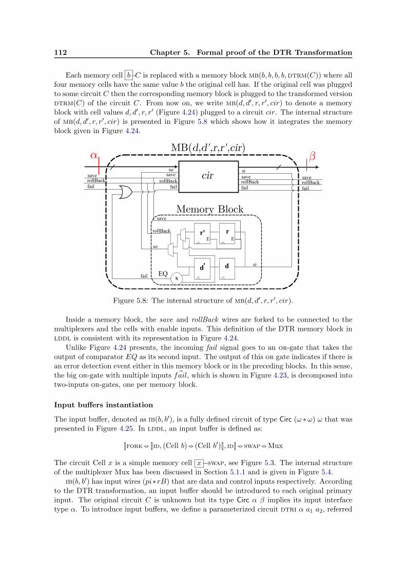
112 Chapter 5. Formal proof of the DTR Transformation
Each memory cell b−C is replaced with a memory block mb(b, b, b, b,dtrm(C)) where allfour memory cells have the same value b the original cell has. If the original cell was pluggedto some circuit C then the corresponding memory block is plugged to the transformed versiondtrm(C) of the circuit C. From now on, we write mb(d, d′, r, r′, cir) to denote a memoryblock with cell values d, d′, r, r′ (Figure 4.24) plugged to a circuit cir. The internal structureof mb(d, d′, r, r′, cir) is presented in Figure 5.8 which shows how it integrates the memoryblock given in Figure 4.24.
save
si
so
rollBack
fail
failfail
si
rollBacksave
so
rollBacksave
EQ
≠
d
rr'
d'
cir
MB(d,d',r,r',cir)
Memory Block
α β
failrollBacksave
failrollBacksave
EE
Figure 5.8: The internal structure of mb(d, d′, r, r′, cir).
Inside a memory block, the save and rollBack wires are forked to be connected to themultiplexers and the cells with enable inputs. This definition of the DTR memory block inlddl is consistent with its representation in Figure 4.24.
Unlike Figure 4.24 presents, the incoming fail signal goes to an or-gate that takes theoutput of comparator EQ as its second input. The output of this or gate indicates if there isan error detection event either in this memory block or in the preceding blocks. In this sense,the big or-gate with multiple inputs ~fail, which is shown in Figure 4.23, is decomposed intotwo-inputs or-gates, one per memory block.
Input buffers instantiation
The input buffer, denoted as ib(b, b′), is a fully defined circuit of type Circ (ω ∗ω) ω that waspresented in Figure 4.25. In lddl, an input buffer is defined as:
[]fork -◦- []id, (Cell b) -◦- (Cell b′)[], id[] -◦- swap -◦- Mux
The circuit Cell x is a simple memory cell x−swap, see Figure 5.3. The internal structureof the multiplexer Mux has been discussed in Section 5.1.1 and is given in Figure 5.4.
ib(b, b′) has input wires (pi∗rB) that are data and control inputs respectively. Accordingto the DTR transformation, an input buffer should be introduced to each original primaryinput. The original circuit C is unknown but its type Circ α β implies its input interfacetype α. To introduce input buffers, we define a parameterized circuit dtri α a1 a2, referred
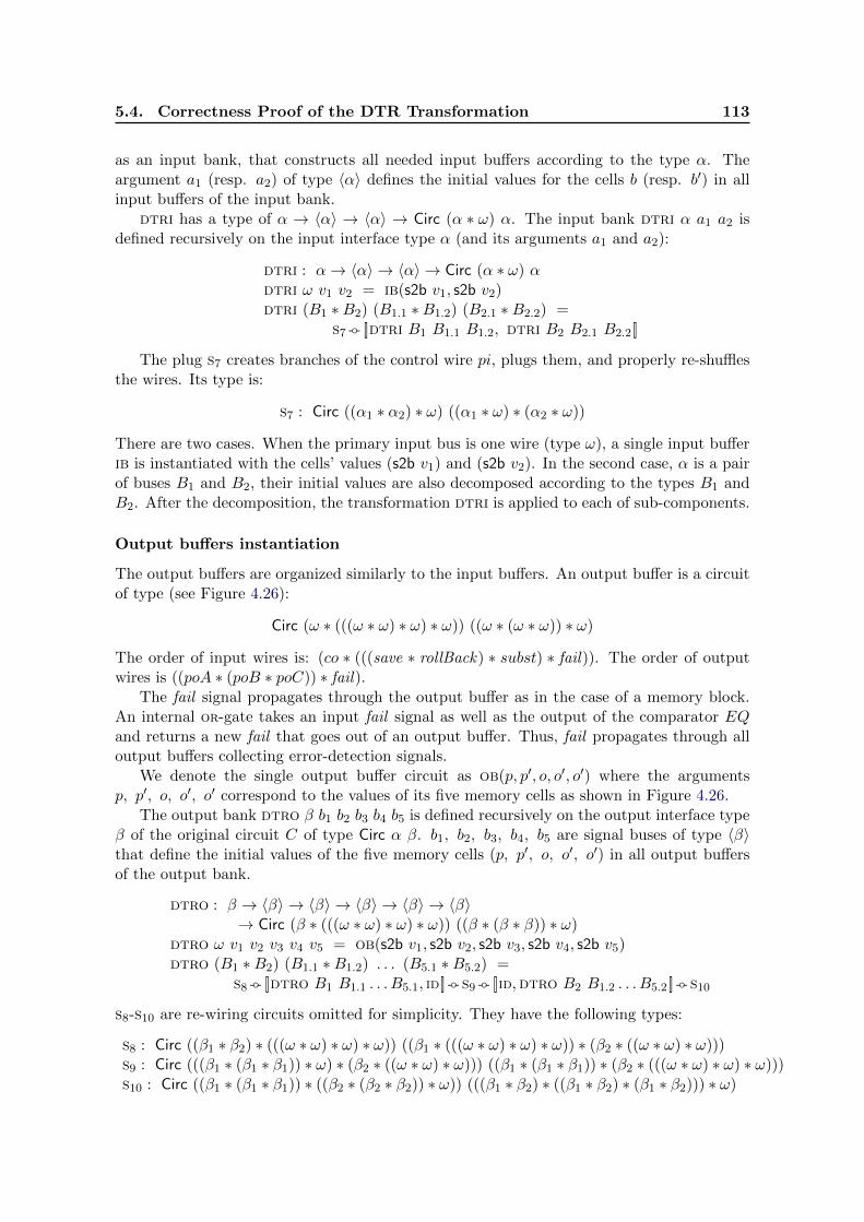
5.4. Correctness Proof of the DTR Transformation 113
as an input bank, that constructs all needed input buffers according to the type α. Theargument a1 (resp. a2) of type 〈α〉 defines the initial values for the cells b (resp. b′) in allinput buffers of the input bank.
dtri has a type of α → 〈α〉 → 〈α〉 → Circ (α ∗ ω) α. The input bank dtri α a1 a2 isdefined recursively on the input interface type α (and its arguments a1 and a2):
dtri : α→ 〈α〉 → 〈α〉 → Circ (α ∗ ω) αdtri ω v1 v2 = ib(s2b v1, s2b v2)dtri (B1 ∗B2) (B1.1 ∗B1.2) (B2.1 ∗B2.2) =
s7 -◦- []dtri B1 B1.1 B1.2, dtri B2 B2.1 B2.2[]
The plug s7 creates branches of the control wire pi, plugs them, and properly re-shufflesthe wires. Its type is:
s7 : Circ ((α1 ∗ α2) ∗ ω) ((α1 ∗ ω) ∗ (α2 ∗ ω))
There are two cases. When the primary input bus is one wire (type ω), a single input bufferib is instantiated with the cells’ values (s2b v1) and (s2b v2). In the second case, α is a pairof buses B1 and B2, their initial values are also decomposed according to the types B1 andB2. After the decomposition, the transformation dtri is applied to each of sub-components.
Output buffers instantiation
The output buffers are organized similarly to the input buffers. An output buffer is a circuitof type (see Figure 4.26):
Circ (ω ∗ (((ω ∗ ω) ∗ ω) ∗ ω)) ((ω ∗ (ω ∗ ω)) ∗ ω)
The order of input wires is: (co ∗ (((save ∗ rollBack) ∗ subst) ∗ fail)). The order of outputwires is ((poA ∗ (poB ∗ poC)) ∗ fail).
The fail signal propagates through the output buffer as in the case of a memory block.An internal or-gate takes an input fail signal as well as the output of the comparator EQand returns a new fail that goes out of an output buffer. Thus, fail propagates through alloutput buffers collecting error-detection signals.
We denote the single output buffer circuit as ob(p, p′, o, o′, o′) where the argumentsp, p′, o, o′, o′ correspond to the values of its five memory cells as shown in Figure 4.26.
The output bank dtro β b1 b2 b3 b4 b5 is defined recursively on the output interface typeβ of the original circuit C of type Circ α β. b1, b2, b3, b4, b5 are signal buses of type 〈β〉that define the initial values of the five memory cells (p, p′, o, o′, o′) in all output buffersof the output bank.
dtro : β → 〈β〉 → 〈β〉 → 〈β〉 → 〈β〉 → 〈β〉→ Circ (β ∗ (((ω ∗ ω) ∗ ω) ∗ ω)) ((β ∗ (β ∗ β)) ∗ ω)
dtro ω v1 v2 v3 v4 v5 = ob(s2b v1, s2b v2, s2b v3, s2b v4, s2b v5)dtro (B1 ∗B2) (B1.1 ∗B1.2) . . . (B5.1 ∗B5.2) =
s8 -◦- []dtro B1 B1.1 . . . B5.1, id[] -◦- s9 -◦- []id,dtro B2 B1.2 . . . B5.2[] -◦- s10
s8-s10 are re-wiring circuits omitted for simplicity. They have the following types:
s8 : Circ ((β1 ∗ β2) ∗ (((ω ∗ ω) ∗ ω) ∗ ω)) ((β1 ∗ (((ω ∗ ω) ∗ ω) ∗ ω)) ∗ (β2 ∗ ((ω ∗ ω) ∗ ω)))s9 : Circ (((β1 ∗ (β1 ∗ β1)) ∗ ω) ∗ (β2 ∗ ((ω ∗ ω) ∗ ω))) ((β1 ∗ (β1 ∗ β1)) ∗ (β2 ∗ (((ω ∗ ω) ∗ ω) ∗ ω)))s10 : Circ ((β1 ∗ (β1 ∗ β1)) ∗ ((β2 ∗ (β2 ∗ β2)) ∗ ω)) (((β1 ∗ β2) ∗ ((β1 ∗ β2) ∗ (β1 ∗ β2))) ∗ ω)
114 Chapter 5. Formal proof of the DTR Transformation
The output bank dtro returns the triplicated output interface (β ∗ (β ∗ β)) and the failsignal.
Control Block
As Figure 4.23 shows, the DTR control block consists of two parts: the control FSM protectedby TMR and three memory cells f1, f2, and f3.
A single copy of the control FSM, denoted ctrFSM(a, b, c), has three internal memorycells a, b, and c to encode its state (see Figure 4.27). ctrFSM(a, b, c) is a sequential circuitof type Circ ω ((((ω ∗ω) ∗ω) ∗ω) ∗ω). The incoming wire is an output of one of the cells f1,f2, or f3. The five outcoming control signals are ((((save ∗ rollBack) ∗ fail) ∗ rB) ∗ subst).The returned fail signal is initialized to zero. It can be set to the logical 1 only in memoryblocks or output buffers where and when an error is detected.
When TMR is applied to ctrFSM(a, b, c), the returned circuit tmr(ctrFSM(a, b, c)) hasthree inputs and three copies of its five control wires. Five voters vot5, one for each triplicatedoutput, are inserted after tmr(ctrFSM(a, b, c)) to mask all possible SETs occurring in itsstructure. As a result, the circuit tmr(ctrFSM(a, b, c)) -◦-vot5 returns five control wires andtakes the three wires from f1, f2, and f3.
From now on, the circuit (tmr(ctrFSM(a, b, c)) -◦-vot5) will be denoted as ctr3(a, b, c)with type Circ ((ω ∗ ω) ∗ ω) ((((ω ∗ ω) ∗ ω) ∗ ω) ∗ ω).
DTR Transformation- Final Definition
Having all aforementioned components, we plug them all together to obtain the final defini-tion of DTR transformation dtr(C) for any circuit C of type Circ α β. The transformationdtr(C) can be expressed as:
dtr(C) ::= f1 − f2 − f3 −(s11 -◦- []id, ctr3(a, b, c)[] -◦- s12 -◦-
[][]dtri α 0α 0α, id[] -◦-dtrm(C), id[] -◦- s13 -◦-
dtro β 0β 0β -◦- s14
), where
the cells f1 − f3 are initialized to false as well as the triple {a, b, c} that denotes the initialstate 0 of the control block (Figure 4.27). The notations 0α and 0β designate the signalbuses of types 〈α〉 and 〈β〉 respectively with all their wires equal to 0. Thus, all memorycells in input dtri and output dtro banks are initialized to false. s11− s14 are plugs thatre-shuffle wires. They have the following types:
s11 : Circ (((α ∗ ω) ∗ ω) ∗ ω) (α ∗ ((ω ∗ ω) ∗ ω))s12 : Circ (α ∗ ((((ω ∗ ω) ∗ ω) ∗ ω) ∗ ω)) (((α ∗ ω) ∗ ((ω ∗ ω) ∗ ω)) ∗ ω)s13 : Circ ((β ∗ ((ω ∗ ω) ∗ ω)) ∗ ω) (β ∗ (((ω ∗ ω) ∗ ω) ∗ ω))s14 : Circ ((β ∗ (β ∗ β)) ∗ ω) (((((β ∗ β) ∗ β) ∗ ω) ∗ ω) ∗ ω)
The transformed circuit dtr(C) has the type Circ α ((β ∗β) ∗β). The triplicated outputinterface of type ((β ∗ β) ∗ β) represents the triplicated original output bus. Figure 5.9graphically represents the structure of the transformed DTR circuit dtr(C).
The three parallel constructions []., .[] in the dtr(C) definition are needed to propagatebuses or control signals to the components where they are used. For instance, since theinput bank does not use the control signals save, rollBack, subst and fail , the construction[]dtri..., id[] propagates these signals (with id) in parallel with the input bank dtri.
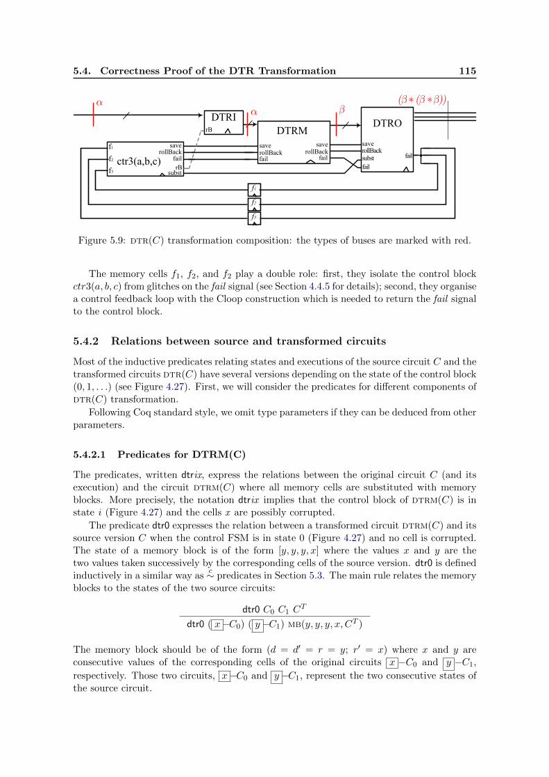
5.4. Correctness Proof of the DTR Transformation 115
DTRIrB
DTRO
saverollBacksubst
f1
f2
f3
DTRM
fail
saverollBack
saverollBack
rBsubst
f1
ctr3(a,b,c)f2
f3
fail fail
saverollBack
fail
fail
α β(β (β β))* *α
Figure 5.9: dtr(C) transformation composition: the types of buses are marked with red.
The memory cells f1, f2, and f2 play a double role: first, they isolate the control blockctr3(a, b, c) from glitches on the fail signal (see Section 4.4.5 for details); second, they organisea control feedback loop with the Cloop construction which is needed to return the fail signalto the control block.
5.4.2 Relations between source and transformed circuits
Most of the inductive predicates relating states and executions of the source circuit C and thetransformed circuits dtr(C) have several versions depending on the state of the control block(0, 1, . . .) (see Figure 4.27). First, we will consider the predicates for different components ofdtr(C) transformation.
Following Coq standard style, we omit type parameters if they can be deduced from otherparameters.
5.4.2.1 Predicates for DTRM(C)
The predicates, written dtrix, express the relations between the original circuit C (and itsexecution) and the circuit dtrm(C) where all memory cells are substituted with memoryblocks. More precisely, the notation dtrix implies that the control block of dtrm(C) is instate i (Figure 4.27) and the cells x are possibly corrupted.
The predicate dtr0 expresses the relation between a transformed circuit dtrm(C) and itssource version C when the control FSM is in state 0 (Figure 4.27) and no cell is corrupted.The state of a memory block is of the form [y, y, y, x] where the values x and y are thetwo values taken successively by the corresponding cells of the source version. dtr0 is definedinductively in a similar way as
c∼ predicates in Section 5.3. The main rule relates the memoryblocks to the states of the two source circuits:
dtr0 C0 C1 CT
dtr0 ( x−C0) ( y −C1) mb(y, y, y, x, CT )
The memory block should be of the form (d = d′ = r = y; r′ = x) where x and y areconsecutive values of the corresponding cells of the original circuits x −C0 and y −C1,
respectively. Those two circuits, x−C0 and y −C1, represent the two consecutive states ofthe source circuit.

116 Chapter 5. Formal proof of the DTR Transformation
While the main rule relates the memory block state with the state of the original cir-cuit, the same predicate dtr0 also relates the other circuit constructions (e.g., gates/plugs,sequential and parallel compositions). For instance, the inference rule for a gate G is:
dtr0 G G []G, id[]
Since the gates are stateless, this relationship always holds if the DTR transformation hasbeen applied to the original gate G: dtr(G)=[]G, id[].
The dtr0 predicate for sequential construction is expressed as:
dtr0 CL C′L C
TL dtr0 CR C ′R CTR
dtr0 (CL -◦-CR) (C ′L -◦-C ′R) (CTL -◦-CTR)
If any two original circuits in two successive states (CL C′L) and (CR C
′R) are in the relation-
ship with two transformed circuits CTL and CTR respectively, then the sequential compositionof these original circuits in these two states (CL -◦-CR) and (C ′L -◦-C ′R) are also in relationwith the transformed circuit (CTL -◦-CTR).
The corresponding predicate when the control FSM is in state 1 relates a transformedcircuit to three successive source circuits. Indeed, in that state, the memory block is of theform [z, y, y, x] where x, y and z are three successive values taken by the corresponding cellof the source circuit. The main rule for the memory block is:
dtr1 C0 C1 C2 CT
dtr1 ( x−C0) ( y −C1) ( z −C2) mb(z, y, y, x, CT )
Several versions of these predicates are needed to represent all the corruption cases. Forinstance, the predicate dtr1d expresses the relation between a transformed circuit whose dcells are potentially corrupted and its source version when the control block is in state 1.The main rule is:
dtr1d C0 C1 C2 CT
dtr1d ( x−C0) ( y −C1) ( z −C2) mb(w, y, y, x, CT )
That is, r′, (resp. d′ and r) should hold the same values are the first (resp. second) sourcecircuit; d is represented by the unconstrained value w; it can be corrupted and take anyvalue. The other rules (for -◦- , []., .[], etc) remain the same as in dtr1.
Other predicates are also needed to relate the source and transformed versions when thecontrol block is in the recovery mode. As we observed in Section 4.4.8, we do no use the cellsd′, r, and r′ during the speed-up mode during the recovery. So, their values are irrelevantduring several cycles i.e., when the control block is in states 2-4. For example, the relationbetween the state of the memory block and the original circuit state is described by thepredicate dtr3:
dtr3 C0 C1 CT
dtr3 ( x−C0) ( y −C1) mb(x,w,w′, w′′, CT )
The values w,w′, w′′ are unconstrained because the cells d′, r, r′ do not participate in thetransformed circuit functionality during the speed-up phase.
5.4. Correctness Proof of the DTR Transformation 117
5.4.2.2 Predicates for DTRI, DTRO, and ctr3
We also define predicates that describe the states of the input/output blocks and the controlblock.
Triplicated control FSM. The states of the triplicated FSM ctr3(a, b, c) can be explicitlylisted:
ctr0 := ctr3(false, false, false)ctr1 := ctr3(false, false, true). . .ctr5 := ctr3(true, false, true)
All these predicates represent the binary encoding of the corresponding FSM states rep-resented in Figure 4.27. For example, ctr1 holds if the control block is in state 1.
Input bank. There are two different cases for an input bank dtri a1 a2:
ibs0(a) := dtri a aibs1(a1, a2) := dtri a1 a2
The first predicate states that the two cells of each input buffer are equal. This is thecase when the control block is in state 0 (Figure 4.27). The second predicate states that thetwo cells may be different. This happens when the control block is in state 1.
Output bank. The output bank dtro b1 b2 b3 b4 b5 has also two predicates, for even andodd clock cycles (states 0 and 1 of the control FSM, Figure 4.27). Recall that the signalbuses (b1, b2, b3, b4, b5) defines values for the cells (p, p′, o, o′, o′′) of output buffers.
obs0(b1, b2) := dtro b1 b1 b1 b1 b2obs1(b1, b2) := dtro b1 b2 b1 b2 b2
obs0 states that in even cycles, each output buffer has the same value in its cells o, o′, p, p′.In odd cycles, the relation between cells are o = p and o′ = o′′ = p′ in each output block.
5.4.2.3 Global DTR predicates
The state of the whole transformed DTR circuit can be described as the combination of theaforementioned predicates relatively to the original circuit C and its consecutive states. Therelation between the complete transformed circuit and its source is described by the followingglobal predicates:
• Dtrs1 and Dtrs0 relate the DTR and source circuit states in the normal mode (states 0and 1 in the control block, Figure 4.27) relatively to the original circuit execution;
• Dtr0d′, Dtr1r and other predicates relate the DTR and source circuit state duringthe recovery procedure and characterize the possible corruption of the different DTRcomponents.
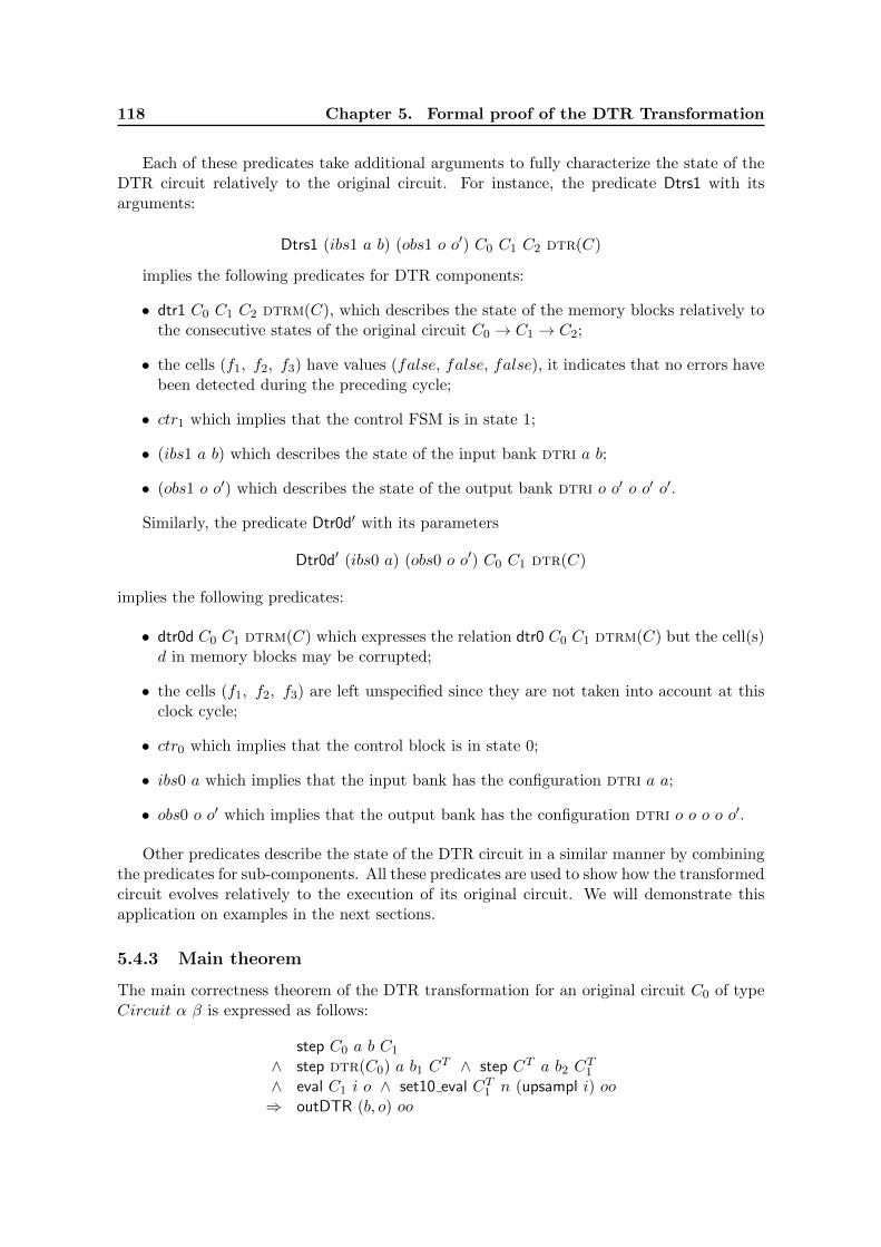
118 Chapter 5. Formal proof of the DTR Transformation
Each of these predicates take additional arguments to fully characterize the state of theDTR circuit relatively to the original circuit. For instance, the predicate Dtrs1 with itsarguments:
Dtrs1 (ibs1 a b) (obs1 o o′) C0 C1 C2 dtr(C)
implies the following predicates for DTR components:
• dtr1 C0 C1 C2 dtrm(C), which describes the state of the memory blocks relatively tothe consecutive states of the original circuit C0 → C1 → C2;
• the cells (f1, f2, f3) have values (false, false, false), it indicates that no errors havebeen detected during the preceding cycle;
• ctr1 which implies that the control FSM is in state 1;
• (ibs1 a b) which describes the state of the input bank dtri a b;
• (obs1 o o′) which describes the state of the output bank dtri o o′ o o′ o′.
Similarly, the predicate Dtr0d′ with its parameters
Dtr0d′ (ibs0 a) (obs0 o o′) C0 C1 dtr(C)
implies the following predicates:
• dtr0d C0 C1 dtrm(C) which expresses the relation dtr0 C0 C1 dtrm(C) but the cell(s)d in memory blocks may be corrupted;
• the cells (f1, f2, f3) are left unspecified since they are not taken into account at thisclock cycle;
• ctr0 which implies that the control block is in state 0;
• ibs0 a which implies that the input bank has the configuration dtri a a;
• obs0 o o′ which implies that the output bank has the configuration dtri o o o o o′.
Other predicates describe the state of the DTR circuit in a similar manner by combiningthe predicates for sub-components. All these predicates are used to show how the transformedcircuit evolves relatively to the execution of its original circuit. We will demonstrate thisapplication on examples in the next sections.
5.4.3 Main theorem
The main correctness theorem of the DTR transformation for an original circuit C0 of typeCircuit α β is expressed as follows:
step C0 a b C1
∧ step dtr(C0) a b1 CT ∧ step CT a b2 C
T1
∧ eval C1 i o ∧ set10 eval CT1 n (upsampl i) oo⇒ outDTR (b, o) oo
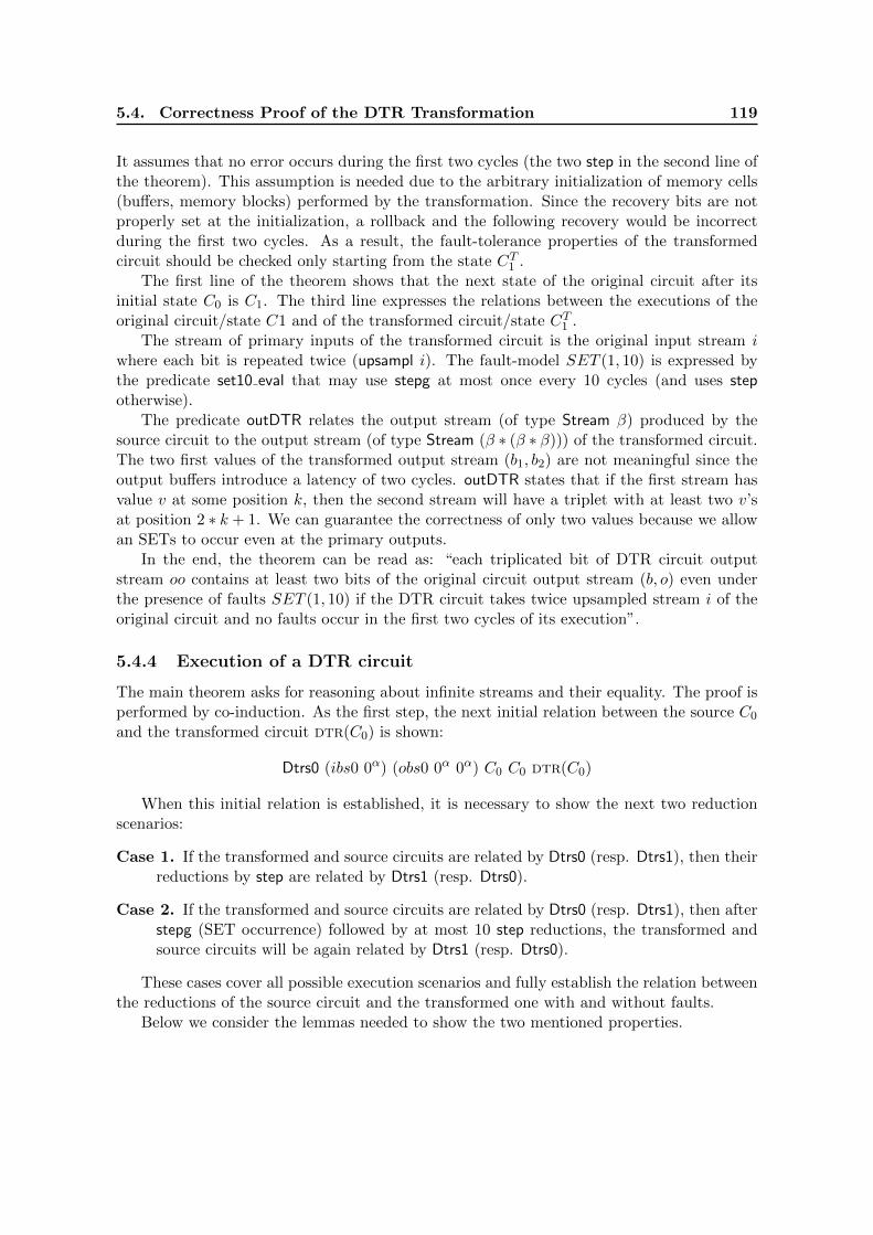
5.4. Correctness Proof of the DTR Transformation 119
It assumes that no error occurs during the first two cycles (the two step in the second line ofthe theorem). This assumption is needed due to the arbitrary initialization of memory cells(buffers, memory blocks) performed by the transformation. Since the recovery bits are notproperly set at the initialization, a rollback and the following recovery would be incorrectduring the first two cycles. As a result, the fault-tolerance properties of the transformedcircuit should be checked only starting from the state CT1 .
The first line of the theorem shows that the next state of the original circuit after itsinitial state C0 is C1. The third line expresses the relations between the executions of theoriginal circuit/state C1 and of the transformed circuit/state CT1 .
The stream of primary inputs of the transformed circuit is the original input stream iwhere each bit is repeated twice (upsampl i). The fault-model SET (1, 10) is expressed bythe predicate set10 eval that may use stepg at most once every 10 cycles (and uses stepotherwise).
The predicate outDTR relates the output stream (of type Stream β) produced by thesource circuit to the output stream (of type Stream (β ∗ (β ∗ β))) of the transformed circuit.The two first values of the transformed output stream (b1, b2) are not meaningful since theoutput buffers introduce a latency of two cycles. outDTR states that if the first stream hasvalue v at some position k, then the second stream will have a triplet with at least two v’sat position 2 ∗ k + 1. We can guarantee the correctness of only two values because we allowan SETs to occur even at the primary outputs.
In the end, the theorem can be read as: “each triplicated bit of DTR circuit outputstream oo contains at least two bits of the original circuit output stream (b, o) even underthe presence of faults SET (1, 10) if the DTR circuit takes twice upsampled stream i of theoriginal circuit and no faults occur in the first two cycles of its execution”.
5.4.4 Execution of a DTR circuit
The main theorem asks for reasoning about infinite streams and their equality. The proof isperformed by co-induction. As the first step, the next initial relation between the source C0
and the transformed circuit dtr(C0) is shown:
Dtrs0 (ibs0 0α) (obs0 0α 0α) C0 C0 dtr(C0)
When this initial relation is established, it is necessary to show the next two reductionscenarios:
Case 1. If the transformed and source circuits are related by Dtrs0 (resp. Dtrs1), then theirreductions by step are related by Dtrs1 (resp. Dtrs0).
Case 2. If the transformed and source circuits are related by Dtrs0 (resp. Dtrs1), then afterstepg (SET occurrence) followed by at most 10 step reductions, the transformed andsource circuits will be again related by Dtrs1 (resp. Dtrs0).
These cases cover all possible execution scenarios and fully establish the relation betweenthe reductions of the source circuit and the transformed one with and without faults.
Below we consider the lemmas needed to show the two mentioned properties.

120 Chapter 5. Formal proof of the DTR Transformation
Case 1. The first two lemmas describe how the transformed circuit evolves relatively tothe execution of the original circuit in normal mode (without SETs). Figure 5.10 illustrates:
1. the execution of an original circuit: C0 → C1 → C2 → C3 → . . .
2. the execution of the corresponding transformed circuit: CT0 → C ′T0 → CT1 → C ′T1 → . . .
Since double time redundancy is used, two cycles of the transformed circuit correspondto one cycle of the source circuit. The relations between executions of the source and trans-formed circuits are described by the predicates Dtrs0 and Dtrs1 (colored polygons in thefigure). The input used during a reduction step is written above the arrow of this step.
C3 C4C0 C0 C2 C3
Dtrs1
Dtrs0C1'
T T ...a a
1 2 3 4 ...
C2C1b b
C0 C1 C2 C3 C4
Dtrs1...a b
T T T T
'T
'T
'T
cc c
dd d...
...
Figure 5.10: DTR circuit step reduction described by predicates.
The first lemma (Case 1. above) can be formalized as:
Lemma 5.3.
Dtrs0 (ibs0 a) (obs0 o o′) C0 C1 CT1 ⇒ step C1 b t1 C2 ⇒ step CT1 b t′1 C
′T1
⇒ t′1 = (o, o, o′) ∧ Dtrs1 (ibs1 b a) (obs1 t1 o) C0 C1 C2 C′T1
We omitted the hypothesis that input signals are pure (i.e., contain no glitch) to makethe theorem less verbose. Lemma 5.3 states that if the transformed circuit CT1
• is in relation by Dtrs0 with the original consecutive circuits states C0 and C1 (redpolygon);
• has its input bank in state (ibs0 a);
• has its output bank in state (obs0 o o′),
then after one clock cycle (step)
• its primary outputs will be (o, o, o′);
• the resulting DTR circuit C ′T1 will be in relation Dtrs1 with the three consecutive statesof the original circuit, C0, C1, and C2 (blue polygon);
• the input bank will be in state (ibs1 b a) meaning that the input signals b have beenfetched and saved in its first cells;
• the output bank will be in state (obs1 t1 o) meaning that the output of combinatorialcircuit t1 has been fetched and saved in it.
5.4. Correctness Proof of the DTR Transformation 121
stepg
...
... C5 C4C0 C0 C2 C5C1
C0 C1 C2 C3 C4
DtrERRDtrs1
Dtrs0
C1...
......
...
aa b ba
b
1 2 3 5 ...
step step step stepT T T T T
'T
'T
'T
Figure 5.11: DTR circuit stepg reduction from the state described by Dtrs0.
This change of the DTR circuit happens when the control block switches from state 0 tostate 1 (Figure 4.27).
During the next clock cycle, the DTR circuit propagates again the same data throughits combinatorial part to produce the second redundant result. Lemma 5.4 describes thecorresponding circuit reduction step:
Lemma 5.4.
Dtrs1(ibs1 b a) (obs1 t1 o) C0 C1 C2 C′T1 ⇒ step C1 b t1 C2 ⇒ step C ′T1 b t′′1 C
T2
⇒ t′′1 = (o, o, o) ∧ Dtrs0 (ibs0 b) (obs0 t1 o) C1 C2 CT2
It states that the transformed circuit C ′T1 returns back from the relations Dtrs1 (bluepolygon) to the relations Dtrs0 (pink polygon) relatively to the consequent states of theoriginal circuit C1 and C2. For both steps the main theorem holds. In particular, its rightside, outDTR (b, o) oo, is true because for both cases at least two of the three output signalsin t′1 and t′′1 equal to o.
The predicates Dtrs0 and Dtrs1 express the relationships of each DTR component rel-atively to the original circuit execution. Thus, the proofs of the aforementioned lemmasrely on the corresponding lemmas about individual DTR components, e.g., input buffers,memory blocks. These properties are described in Section 5.4.5.
Case 2. If the transformed circuit reduces by stepg, then the proof considers all possiblecorruption scenarios. The reduction by stepg of the DTR circuit CT1 may return severalcorrupted circuits {C ′T1 }. Each returned circuit C ′T1 is in a distinct relationship with thesource circuit. They are described by a predicate for each corruption case. Figure 5.11represents such a case with a (generic) predicate DtrERR.
It can be shown that, in all these corruption scenarios, the DTR circuit returns to acorrect state within ten clock clocks. More precisely, after ten cycles, the relation betweenthe DTR and source circuits is either Dtrs0 or Dtrs1.
A stepg reduction of CT1 can lead to the corruptions listed in Table 5.4.4.Recall that memory cells r and r′ with enable inputs save are organized by introducing
a multiplexer in front of a flip-flip, see Figure 5.12. This multiplexer is denoted MuxE in thetable and represents a potential point of fault injection for stepg.
All in all, there are 13 different corruption cases. Among all the listed cases, consider indetails the case when the global save signal is corrupted by an SET after the control block.The glitched save may corrupt only memory cells r and r′ in memory blocks. This possiblecorruption case of memory blocks is described by the predicate Dtr1rr′. This predicate
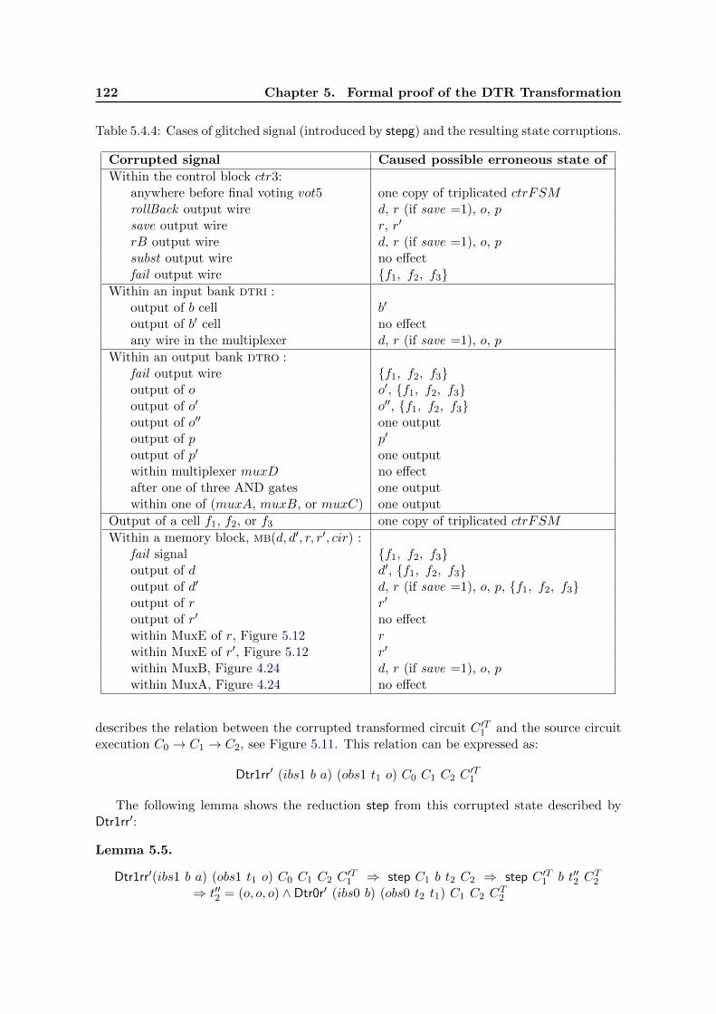
122 Chapter 5. Formal proof of the DTR Transformation
Table 5.4.4: Cases of glitched signal (introduced by stepg) and the resulting state corruptions.
Corrupted signal Caused possible erroneous state of
Within the control block ctr3:anywhere before final voting vot5 one copy of triplicated ctrFSMrollBack output wire d, r (if save =1), o, psave output wire r, r′
rB output wire d, r (if save =1), o, psubst output wire no effectfail output wire {f1, f2, f3}
Within an input bank dtri :output of b cell b′
output of b′ cell no effectany wire in the multiplexer d, r (if save =1), o, p
Within an output bank dtro :fail output wire {f1, f2, f3}output of o o′, {f1, f2, f3}output of o′ o′′, {f1, f2, f3}output of o′′ one outputoutput of p p′
output of p′ one outputwithin multiplexer muxD no effectafter one of three AND gates one outputwithin one of (muxA, muxB, or muxC) one output
Output of a cell f1, f2, or f3 one copy of triplicated ctrFSM
Within a memory block, mb(d, d′, r, r′, cir) :fail signal {f1, f2, f3}output of d d′, {f1, f2, f3}output of d′ d, r (if save =1), o, p, {f1, f2, f3}output of r r′
output of r′ no effectwithin MuxE of r, Figure 5.12 rwithin MuxE of r′, Figure 5.12 r′
within MuxB, Figure 4.24 d, r (if save =1), o, pwithin MuxA, Figure 4.24 no effect
describes the relation between the corrupted transformed circuit C ′T1 and the source circuitexecution C0 → C1 → C2, see Figure 5.11. This relation can be expressed as:
Dtr1rr′ (ibs1 b a) (obs1 t1 o) C0 C1 C2 C′T1
The following lemma shows the reduction step from this corrupted state described byDtr1rr′:
Lemma 5.5.
Dtr1rr′(ibs1 b a) (obs1 t1 o) C0 C1 C2 C′T1 ⇒ step C1 b t2 C2 ⇒ step C ′T1 b t′′2 C
T2
⇒ t′′2 = (o, o, o) ∧ Dtr0r′ (ibs0 b) (obs0 t2 t1) C1 C2 CT2
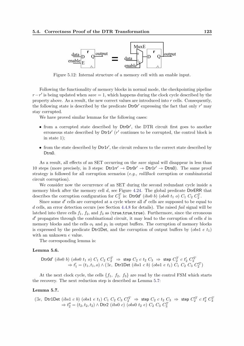
5.4. Correctness Proof of the DTR Transformation 123
= 1
0
cQ
rDE
Q Qr
D Q
enable
data output
enable dataoutput
MuxE
Figure 5.12: Internal structure of a memory cell with an enable input.
Following the functionality of memory blocks in normal mode, the checkpointing pipeliner−r′ is being updated when save = 1, which happens during the clock cycle described by theproperty above. As a result, the new correct values are introduced into r cells. Consequently,the following state is described by the predicate Dtr0r′ expressing the fact that only r′ maystay corrupted.
We have proved similar lemmas for the following cases:
• from a corrupted state described by Dtr0r′, the DTR circuit first goes to anothererroneous state described by Dtr1r′ (r′ continues to be corrupted, the control block isin state 1);
• from the state described by Dtr1r′, the circuit reduces to the correct state described byDtrs0.
As a result, all effects of an SET occurring on the save signal will disappear in less than10 steps (more precisely, in 3 steps: Dtr1rr′ → Dtr0r′ → Dtr1r′ → Dtrs0). The same proofstrategy is followed for all corruption scenarios (e.g., rollBack corruption or combinatorialcircuit corruption).
We consider now the occurrence of an SET during the second redundant cycle inside amemory block after the memory cell d, see Figure 4.24. The global predicate DtrERR thatdescribes the corruption configuration for CT2 is: Dtr0d′ (ibs0 b) (obs0 t1 o) C1 C2 C
T2 .
Since some d′ cells are corrupted at a cycle where all d′ cells are supposed to be equal tod cells, an error detection occurs (see Section 4.4.8 for details). The raised fail signal will belatched into three cells f1, f2, and f3 as (true,true,true). Furthermore, since the erroneousd′ propagates through the combinational circuit, it may lead to the corruption of cells d inmemory blocks and the cells o1 and p1 in output buffers. The corruption of memory blocksis expressed by the predicate Dtr1Det, and the corruption of output buffers by (obs1 e t1)with an unknown e value.
The corresponding lemma is:
Lemma 5.6.
Dtr0d′ (ibs0 b) (obs0 t1 o) C1 C2 CT2 ⇒ step C2 c t2 C3 ⇒ step CT2 c t′2 C
′T2
⇒ t′1 = (t1, t1, o) ∧ (∃e, Dtr1Det (ibs1 c b) (obs1 e t1) C1 C2 C3 C′T2 )
At the next clock cycle, the cells {f1, f2, f3} are read by the control FSM which startsthe recovery. The next reduction step is described as Lemma 5.7:
Lemma 5.7.
(∃e, Dtr1Det (ibs1 c b) (obs1 e t1) C1 C2 C3 C′T2 ⇒ step C2 c t2 C3 ⇒ step C ′T2 c t′′2 C
T3
⇒ t′′2 = (t2, t2, t2) ∧ Dtr2 (ibs0 c) (obs0 t2 e) C2 C3 CT3

124 Chapter 5. Formal proof of the DTR Transformation
The predicate Dtr2 expresses the fact that the predicate ctr2 holds (the control block isin state 2). The newly recalculated combinational circuit output t2 is directly propagatedto the primary output of the DTR circuit. During the following 8 clock cycles, the recoveryhappens. Each state of the DTR circuit is related to the original circuit execution with adedicated predicate. In the end, we show that the state of the circuit returns to the predicateDtrs0 that holds in the normal mode.
All the aforementioned properties, expressed as Coq theorems, rely on the properties ofDTR components such as memory blocks, input and output buffers, etc. These propertiesare considered in the next section.
5.4.5 Lemmas on DTR components
The previous section discussed how to prove the main theorem by showing how the trans-formed circuit evolves with and without faults relatively to the original circuit execution. Theproofs of these properties rely on lemmas that show how the components of the transformedcircuit evolve. For instance, to prove Lemma 5.3, it is necessary to show that:
• the dtrm component reduces from dtr0 to dtr1;
• the control block evolves from the state ctr0 to ctr1;
• the input bank dtri reduces from (ibs0 a) to (ibs1 b a) where b is the new primaryinput;
• the output bank dtro reduces from (obs0 a b) to (ibs1 c b) where c is the currentoutput of the combinational circuit.
5.4.5.1 Lemmas for DTRM
Consider the following property for the reduction of dtrm component CT with no SET:
Lemma 5.8.
dtr0 C0 C1 CT ⇒ step C1 a b C2 ⇒ step CT {a, {0, 0, 0}} b′ C ′T⇒ b′ = {b, {0, 0, 0}} ∧ dtr1 C0 C1 C2 C
′T
It states that, if the original circuit evolves from C1 to C2 with input a, then the cor-responding transformed circuit CT with input a and signals save = 0, rollBack = 0, andfail = 0 returns the same output b and leaves the global signals unchanged. Further, if CT
is related to (C0, C1) with dtr0, the returning state C ′T is related to (C0, C1, C2) with dtr1.The mirror property from dtr1 to dtr0 relations can be expressed as:
Lemma 5.9.
dtr1 C0 C1 C2 CT ⇒ step C1 a b C2 ⇒ step CT {a, {1, 0, f}} b′ C ′T
⇒ ∃f, b′ = {b, {1, 0, f}} ∧ dtr0 C1 C2 C′T
It shows how the transformed circuit CT evolves into C ′T during even clock cycles rela-tively to the states of the original circuit. In normal mode, the save control signal is set (forcheckpointing) and the fail signal is irrelevant (i.e., f is existentially quantified).
Above, we have considered the corruption scenario when a glitched save signal corruptsthe checkpointing memory cells r and r′ in memory block. Consider the same reduction stepwith the corrupted save signal but for dtrm component, we can prove Lemma 5.10:

5.4. Correctness Proof of the DTR Transformation 125
Lemma 5.10.
dtr0 C0 C1 CT ⇒ step C1 a b C2 ⇒ step CT {a, {�, 0, 0}} b′ C ′T⇒ b′ = {b, {�, 0, 0}} ∧ dtr1rr′ C0 C1 C2 C
′T
The property can be read as: if an original circuit C1 with input a reduces to thecircuit C2, then the corresponding transformed circuit CT with data input a, rollBack =fail = 0 and a glitched save signal will return a circuit C ′T where memory cells r and r′ inmemory blocks are possibly corrupted. The overall proof uses 28 such lemmas correspondingto the different corruption cases of memory blocks.
All such properties are shown by simple structural induction.
5.4.5.2 Lemmas for input and output buffers (DTRI, DTRO)
Since input and output buffers are known circuit, properties on them are easily proven usingreflection. For instance, one of the lemmas describes how the state of an output buffer evolvesin the normal mode:
Lemma 5.11.
pure a ⇒ step ob(p1, p2, o1, o2, o3) {a, {save, 0, fail , 0}} b C ′ ⇒b = {b2s p2, {b2s o2, b2s o3},or{fail , b2s(xor o1 o2)}} ∧ C ′ = ob((s2b a), p1, (s2b a), o1, o2)
It states that, if the data input a of an output buffer is not corrupted by an SET (predicatepure a), it will be latched by the cells o and p as (s2b a). The values p1, o1, and o2 arepropagated and latched by the following cells p′, o′, and o′′ respectively. The value of theoutgoing fail signal is defined by the expression or {fail , b2s(xor o1 o2)} which formalizesthe error detection mechanism in the output buffer (Figure 4.26). The data primary outputspoA, poB, and poC (Figure 4.26) return the values of the memory cells p′, o′, and o′′ andare respectively equal to b2s p2, b2s o2, and b2s o3.
In the case of an SET during even cycles, the following lemma describes the behavior ofan output buffer:
Lemma 5.12.
stepg ob(b, b′, b, b′, b′) {b2s b, {1, 0, b2s f, 0}} o C ′ ⇒(∃ x, o = {x, {b2s b′, b2s b′}, } ∨ o = {b2s b′, {x, b2s b′}, } ∨ o = {b2s b′, {b2s b′, x}, })∧(∃ z, C ′ = ob(b, z, b, b, b′) ∨ C ′ = ob(b, b, b, z, b′) ∨ C ′ = ob(b, b, b, b, z))
The initial values of the cells o′, o′′, and p′ are the same and equal to b′ according to theoutput buffers functionality. If an SET occurs in an output buffer (stepg reduction), thereare three possible corruption scenarios for the outputs and for the internal state. Accordingto this lemma, only one of three data outputs can be corrupted by an SET (stepg reduction),the other two are correct and equal to b2s b′.
Since during even cycles the fail signal can be ignored, the property does not specifywhat value the returned fail signal should have (denoted by ′ ′).
There are three cases of possible internal state corruption: C ′ = ob(b, z, b, b, b′), C ′ =ob(b, b, b, z, b′), or C ′ = ob(b, b, b, b, z). Only one of the cells {o′, o′′, p′} may takean unknown possibly corrupted value z as a result of an SET. The cells o and p cannot becorrupted in this case. Their corruption can be caused only by a glitch on the input data
126 Chapter 5. Formal proof of the DTR Transformation
wire which can be introduced only by the circuit providing this data wire (e.g., a glitch onthe memory block output wire so, see Figure 4.24).
The main advantage of reflection-based proofs is their automatization. In the case ofstepg, all possible SET insertion cases are generated and the correctness of the implicationis checked in an automatic manner.
The properties for the input bank dtri (resp. output bank dtro) are proved by inductionon its type and rely on the corresponding lemmas for the individual input ib (resp. outputob) buffer. The previous property for an output bank dtro can be written as:
Lemma 5.13.
stepg (dtro v v′ v v′ v′) {v, {1, 0, f, 0}} o C ′ ⇒(∃ x, o = {x, {v′, v′}, } ∨ o = {v′, {x, v′}, } ∨ o = {v′, {v′, x}, })∧(∃ z, pure z ∧ ((C ′ = dtro v z v v v′) ∨ (C ′ = dtro v v v z v′) ∨ (C ′ = dtro v v v v z)))
5.4.5.3 Lemmas for the control block
The properties of the triplicated control block, ctr3(a, b, c), can be classified into two cate-gories:
1. the states of its three redundant modules are equal;
2. there is one redundant module whose state differs from the states of two others.
The properties of the first group are proven by reflection due to the simplicity of this proofstrategy. Alternatively, they could be proven using properties of the TMR transformationand the lemmas about the reduction step of its one redundant copy, called ctrFSM(a, b, c)(see Section 5.4.1).
The lemmas in the second category make a critical use of the main properties provedfor the TMR transformation. They show how the control block ctr3(a, b, c) recovers from acorrupted state or, vice versa, how it can be corrupted.
As an example, consider the control block where one redundant copy of its triplicatedFSM is corrupted. This sort of corruption is described by the next relation:
ctrFSM(false, false, true)c∼ ctrTMR (see Section 5.3.2 for details)
It can be read as: “the triplicated FSM ctrTMR contains two modules in the state (false,false, true) while its third module has an unknown state”. In this case, the whole controlblock with its output voters is expressed as the circuit ctrTMR -◦-vot5. The next lemmashows that this corrupted control block is reduced in one step to the correct circuit statectr3(false, false, false) and the correct output ttt:
Lemma 5.14.
ctrFSM(false, false, true)c∼ ctrTMR ⇒ step (ctrTMR -◦-voter5) {0, 0, 0} ttt C ′ ⇒
ttt = {0, 0, 0, 0, 0} ∧ C ′ = ctr3(false, false, false)
This property is proven thanks to the Lemma 5.2 (Section 5.3.3) which describes thegeneral characteristic of the TMR transformation, in particular: “if one redundant copy ofthe TMR circuit is corrupted, the next circuit state of this TMR design will be correct aswell as its outputs”.
5.5. Conclusion 127
5.5 Conclusion
To the best of our knowledge, our work is the first to certify automatic circuit transformationsfor fault-tolerance. If some works prove fault-tolerance for known circuits using ITPs [133,134], our approach can show fault-tolerance for any resulting transformed circuit “once andfor all”. Contrary to most of the verification works which specify particular circuits withinthe logic of the prover, we use a gate-level HDL, called lddl. This approach allows us tomodel SETs in the semantics of lddl. Our DTR technique is easily specified by programtransformations on the syntax of lddl. Furthermore, its variable-less nature allowed a simplesemantics (without environments) that facilitated formalization and proofs.
Our approach is general and applicable to many fault-tolerant transformations. In thisdissertation, we used it to prove the correctness of the DTR transformation whose correctnesswas far from obvious. While we relied on many manual checks to design the transformation(Section 4.4), only Coq allowed us to get a complete assurance. The formalization of DTRdid not reveal real errors but a few imprecisions. For instance, we stated in [20] that thecontrol block was protected using TMR without making it clear how it was connected to therest of the circuit. We had to introduce three cells f1, f2, f3 in front of the triplicated controlFSM (Figure 4.23) to record the value of the fail signal. These three cells prevent a glitchfrom propagating simultaneously to the three redundant modules of the FSM. If these cellswere not introduced, the glitch would put the three redundant FSMs into three differentstates which would prohibit proper recovery. The introduction of these cells required toslightly change the definition of the internal FSM.
Our proof approach makes an essential use of two features of Coq: dependent types andreflection. Dependent types provided an elegant solution to ensure that all circuits were well-formed. Such types are often presented as tricky to use but, in our case, that complexityremained confined to the writing of libraries for the equality and decomposition of buses andcircuits. Reflection was very useful to prove properties of known sub-circuits; it would hadbeen much harder without it.
The size of the specifications and proofs for DTR is 7000 lines of Coq. Checking allthe proofs takes around 45 min on an average laptop. Completing the proof of DTR tookroughly 4 or 5 man-months. The Coq files for these proofs are available online [156].


Chapter 6
Conclusions
6.1 Summary
In this dissertation, we have shown how to design, optimize, and verify circuit fault-tolerancetechniques using formal methods. Formal methods guarantee functional correctness and theabsence of failures w.r.t. a fault-model. Such assurance is more than needed when circuitsare used in safety-critical domains such as aerospace, defense, and nuclear industries wherethe cost of design mistakes is really high.
We have demonstrated how static analyses can be used for optimization of fault-tolerantdesigns. In particular, we investigated how majority voters can be removed from TMRcircuits without violating fault-tolerance properties [15]. We extended the standard two-value logic domain in order to represent faults and encoded a circuit and its input/outputinterface specification as a single transition system. Our static, BDD-based, symbolic analysisdemonstrated that, in practice, many voters can be safely removed. While we ran into theexpected state explosion problem, we have explicitly shown that the optimization is effectivefor average size circuits (< 100 memory cells).
We proposed flexible alternatives to TMR that require less hardware resources and couldbe easily applied and integrated in EDA tools. Proposing the TTR transformation andimproving it, we have designed a whole family of time-redundant circuit transformationsfor fault-tolerance. We introduced a novel principle, called dynamic time redundancy, thatallows the transformed circuit to change the order of time-redundancy “on-the-fly” with-out interrupting the computation [19]. The transformed circuit can dynamically adapt thethroughput/fault-tolerance trade-off by changing its redundancy level. Therefore, time-redundancy can be used only in critical situations, during the processing of crucial data,or critical processes. Merging this principle with a micro-checkpointing mechanism, we havecreated a double-time redundant technique capable to mask faults with a fast and transparentrecovery procedure [20]. The corresponding circuit transformation, called DTR, makes anycircuit tolerant to the fault-model SET (1, 10). The throughput of a DTR circuit is 50-55% ofthe corresponding TMR circuit alternative. However, other time-redundant error-correctingtechniques like TTR have even higher throughput loss. According to our experiments, DTRcircuits are 1.9 to 2.5 times smaller than their TMR counterparts. DTR is an interestingalternative to TMR in applications where hardware size constraints are more stringent thanhigh-performance constraints.
We have checked the properties of TTR, dynamic time redundancy transformations, andDTR manually investigating each fault scenario. Nevertheless, due to the complexity of DTRand the great number of possible fault cases, such checks could not provide full assurance.The only way to resolve this issue was to use formal proofs.
We have proposed a language-based approach to formally certify the functional andfault-tolerance properties of circuit transformations using the Coq proof assistant [21]. Weintroduce the syntax and semantics of a simple gate-level functional HDL, called lddl, todescribe circuits. The fault-model (e.g., SET (1,K)) is formalized in lddl semantics. An
130 Chapter 6. Conclusions
automatic fault-tolerance transformation, like DTR, is easily specified as recursive functionson the syntax of lddl. The correctness proof shows the relations between the output streamof a transformed circuit that experiences faults and the output stream of its original circuitwithout faults. Around 7000 Coq lines and 5 man-months were required to show DTRcorrectness. To the best of our knowledge, our work is the first to certify automatic circuittransformations for fault-tolerance.
6.2 Future Work
Hereafter, we discuss further research directions that have been inspired by the results ob-tained in this dissertation.
Voter-minimization for higher frequency. In our verification-based approach for vot-ers suppression, we had to choose the order in which voters are analyzed (Section 3.3.2).This order could also take into account other optimization criteria than voter minimization.Another useful optimization is to increase the maximum synthesizable frequency by remov-ing first the voters on the critical path. However, removing a voter from the critical pathmay make another path critical. Thus, the choice of the next voter to remove depends notonly on the existing ordering but also on the current critical path. However, the critical pathstrategy may not lead to a minimal number of voters. In this sense, the two criteria “numberof voters” and “synthesizable frequency” are orthogonal, and bi-criteria optimization mustbe studied.
Modularity of voter-minimization analysis. Applying our analysis in a modular man-ner would increase its scalability and, consequently, the applicability of the proposed tech-nique to larger circuits. The hierarchical compositional design of today’s circuits makes itnatural to decompose a circuit to the IPs of its block-by-block structure. Such structuralpartitioning requires a deep understanding of the design. It has already been used in themodel checking of Intel CPUs [159]. In our case, the presented analysis can be applied tocircuit sub-components after the decomposition. After the minimization of internal votersin each sub-circuit, the components should be interconnected again to rebuild the wholedesign. However, the interconnection wires should include voters to guarantee the fault-tolerance property of the final optimized circuit. Such an approach is not optimal even ifthe local input/output specifications are precise, because some of the interconnection votersmay be redundant. Only a global analysis can safely remove such voters.
If a decomposition in sub-circuits is not known, the circuit netlist has to be automaticallydivided and the input-output specifications of its parts have to be figured out. These steps areby themselves complex and require deep investigation. Here, we just sketch some preliminaryideas. First, a circuit netlist can be separated according to some syntactic criteria. Forexample, the circuit cuts could be performed at wires that are included in the largest numberof sequential loops. Such an approach eliminates as many sequential loops as possible byreducing the number of sequential loops in each sub-component. It limits the number ofpotential points where the voters have to be inserted.
After the circuit decomposition, our semantic analysis can be applied to each of its sub-parts. The main difficulty lies in the identification of input/output specification of eachsub-circuit to perform the local semantic analyses. Figure 6.1 presents three cases of circuitseparation:

6.2. Future Work 131
c1 c2 c1c2
a) b)
c)
i2c1
i1 o1 o2
c2Figure 6.1: a) Sequential, b) parallel, and c) feedback circuit decomposition.
While the input/output specification for c1 and c2 sub-circuits can easily be extractedfrom the global specification for the parallel decomposition (case b, Fig. 6.1), the sequentialand feedback decompositions (cases a and c) create unknown internal specifications (markedin red). They have to be computed or approximated for each sub-part. Consider, for instance,the unknown input specification i2 for the sequential decomposition (case a). The signals in i2are the outputs o1. Since the netlist c1 and its input specification i1 fully describe the behaviorof c1, o1 and i2 can be described by the same NBA. In the worst case, such NBA could beas big as c1 multiplied by the size of i1, which can be prohibitive for the following semanticanalysis of c2 sub-circuit. Consequently, the extracted NBA should be over-approximatedto lower the complexity. The feedback decomposition is even more complex because of themutual dependency between sub-components c1 and c2.
These modularity issues are complex but important and valuable since many other staticanalyses of circuits could benefit from them.
Time-redundancy techniques frequency optimization. Chapter 4 introduced thefamily of time-redundant techniques that trade circuit throughput off for small hardwareoverhead. A possible research direction is to increase the maximum synthesizable frequencyof the transformed circuits to partially compensate the throughput loss. All presented tech-niques have pipelined structures in their memory blocks, which may allow optimizationsusing retiming. Moving the pipeline memory cells into the combinational circuit could breakthe critical path and increase the synthesizable frequency. For instance in DTR, the memorycells r and d might be moved into the combinatorial circuit; the same can be done with thecells d and d′ in TTR.
Transient faults on the clock line. Throughout the dissertation, we assume that tran-sient faults can happen only on data wires. We did not consider glitches on the clock line,while they may present a danger and lead to simultaneous multi-bit data corruptions. Sev-eral independent but synchronous clocks lines could be used to prevent non-recoverable bitscorruption. For instance, in the DTR scheme, the memory cells (d, d′) could use two differ-ent clocks to avoid their simultaneous corruption by an SET on their common clock line thatwould prohibit any error-detection (Figure 4.24). It is necessary to consider all combinations

132 Chapter 6. Conclusions
of simultaneous memory cells corruption to propose solutions that minimize the number ofclock lines but, at the same time, guarantee fault-tolerance.
Tolerances to multiple faults. Another research direction lies in the extension of thepresented transformations to deal with several simultaneous soft-errors. While it is necessaryto increase the order of redundancy to be able to detect/mask simultaneous faults, thecombination of time-redundancy with checkpointing/rollback mechanisms may allow us toreduce the throughput loss. For instance, using triple-time redundancy with the check-pointing/rollback scheme inspired from DTR, it could be possible to mask two simultaneousSETs. Since triple-time redundancy allows us to detect up to two simultaneous errors,the normal mode will be triple-time redundant. If an error is detected, the rollback will beperformed to the previous correct state. Note that the circuit cannot decide if it has detectedone or two errors in redundant bits-triples. Thus, to be on a safe side, the re-computationafter the rollback will be done in double-time redundant mode that offers error-detectioncapabilities. If no errors have been detected during this double-time redundant recoveryphase, the circuit will eventually return to its normal state that it would have had if no errorhad been detected. If another error is detected during this double-time redundant recoveryphase, another rollback will be needed after which time-redundancy can be switched-off forthe following recovery because two faults have already happened and been detected. Thus,we could obtain stronger fault-tolerance properties than what TTR provides, but with thesame throughput loss. Further investigation and checks remain necessary.
Techniques combination. Further research could consider the combination of differentcircuit transformations for fault-tolerance, such as TMR and DTR. We believe that the circuittransformations could be adjusted so that their consecutive applications will lead to strongerfault-tolerance properties than the properties of individual transformations. Unfortunately,their straightforward application does not lead to this desired result. If we apply TMR toa DTR circuit, then we obtain the properties of the latest transformation losing all benefitsof the checkpointing/rollback mechanism. Similarly, DTR can be applied to TMR circuitsbut the resulting fault-tolerance properties will not be better than the properties of DTR.Further studies may lead to new fault-tolerant solutions with unique characteristics.
Automatization of formal proofs. We believe that additional user-defined Coq tacticscould make the proofs of circuit transformations in lddl (Chapter 5) automatic and muchshorter. Indeed, the key parts are to define the predicates relating the source and transformedcircuits and to state the lemmas. The proofs themselves are, for the most part, straightfor-ward inductions. The proposed framework could also be used to prove other fault-tolerancemechanisms, such as the transformations for dynamic time-redundancy that we presented inSection 4.3 or well-known techniques used in circuit synthesis such as FSM-encoding.
While this dissertation reveals only a small part of how fault-tolerance techniques can bedesigned, optimized, and formally verified, we have a strong belief that further integrationof formal methods in the design flow and circuit analysis will lead to new fault-tolerancetechniques. Such integration eliminates all doubts about the correctness of the techniques,which, hopefully, will increase the speed of their introduction into industrial safety-criticalprojects and tools. We hope that this dissertation can inspire others people to pay attentionto such promising multi-disciplinary domain as formally verified fault-tolerant circuit design.
Bibliography
[1] Wassim Mansour. Methodes et outils pour l’analyse tot dans le flot de conception dela sensibilite aux soft-erreurs des applications et des circuits integres. In PhD thesis,October 2012.
[2] T. Austin, D. Blaauw, T. Mudge, and K. Flautner. Making typical silicon matter withRazor. Computer, 37(3):57–65, March 2004.
[3] M. Nicolaidis. Time redundancy based soft-error tolerance to rescue nanometer tech-nologies. In 17th IEEE VLSI Test Symposium, pages 86–94, 1999.
[4] Kenneth S. McElvain. Circuits with modular redundancy and methods and apparatusesfor their automated synthesis. Synplicity, Inc. Patent No.US007200822B1, April 2007.
[5] Altera Corporation and Micron Technology. Error correction code in SoC FPGA-basedmemory systems. WP-01179-1.2, April 2012.
[6] Steven P. Miller and Mandayam K. Srivas. Formal verification of the AAMP5 mi-croprocessor: a case study in the industrial use of formal methods. In Workshop onIndustrial-Strength Formal Specification Techniques, pages 2–16, 1995.
[7] Neutron-induced Single Event Upset SEU. Microsemi Corporation, (55800021-0/8.11),August 2011.
[8] P.D. Bradley and E. Normand. Single event upsets in implantable cardioverter defib-rillators. IEEE Transactions on Nuclear Science, 45(6):2929–2940, Dec 1998.
[9] P. Shivakumar, M. Kistler, S.W. Keckler, D. Burger, and L. Alvisi. Modeling the effectof technology trends on the soft error rate of combinational logic. In Int. Conferenceon Dependable Systems and Networks, pages 389–398, 2002.
[10] Brendan Bridgford, Carl Carmichael, and Chen Wei Tseng. Single-event upset mitiga-tion selection guide. Xilinx Application Note XAPP987, 1, 2008.
[11] Angela Sutton. Creating highly reliable FPGA designs. Military&Aerospace TechnicalBullentin, 1:5–7, 2013.
[12] Roger D. Do. New tool for FPGA designers mitigates soft errors within synthesis.Mentor Graphics, Inc., December 2011.
[13] C. Chan, D. Schwartz-Narbonne, D. Sethi, and S. Malik. Specification and synthesis ofhardware checkpointing and rollback mechanisms. In Design Automation Conference,pages 1222–1228, 2012.
[14] Dirk Koch, Christian Haubelt, and Jurgen Teich. Efficient hardware checkpointing:Concepts, overhead analysis, and implementation. Proceedings of the ACM/SIGDAInternational Symposium on Field-Programmable Gate Arrays, pages 188–196, 2007.
[15] Dmitry Burlyaev, Pascal Fradet, and Alain Girault. Verification-guided voter mini-mization in triple-modular redundant circuits. In Design, Automation & Test in EuropeConference & Exhibition, pages 1–6, 2014.

134 Bibliography
[16] J.M. Johnson and M.J. Wirthlin. Voter insertion algorithms for FPGA designs usingtriple modular redundancy. In International Symposium on Field Programmable GateArrays, FPGA, pages 249–258. ACM, 2010.
[17] B. Baykant Alagoz. Fault masking by probabilistic voting. OncuBilim Algorithm AndSystems Labs, 9(1), 2009.
[18] P.K. Samudrala et al. Selective triple modular redundancy based single-event upsettolerant synthesis for FPGAs. IEEE Trans. on Nuclear Science, pages 284 – 287,October 2004.
[19] Dmitry Burlyaev, Pascal Fradet, and Alain Girault. Time-redundancy transformationsfor adaptive fault-tolerant circuits. In NASA/ESA Conf. in Adaptive Hardware andSystems, AHS, June 2015.
[20] Dmitry Burlyaev, Pascal Fradet, and Alain Girault. Automatic time-redundancy trans-formation for fault-tolerant circuits. In Proceedings of the ACM/SIGDA InternationalSymposium on Field-Programmable Gate Arrays, pages 218–227, 2015.
[21] Dmitry Burlyaev and Pascal Fradet. Formal verification of automatic circuit transfor-mations for fault-tolerance. In Formal Methods in Computer-Aided Design, FMCAD,September 2015.
[22] Subhasish Mitra, Norbert Seifert, Ming Zhang, Quan Shi, and Kee Sup Kim. Ro-bust system design with built-in soft-error resilience. IEEE Computer, 38(2):43–52,February 2005.
[23] Algirdas Avizienis, Jean-Claude Laprie, Brian Randell, and Carl Landwehr. Basicconcepts and taxonomy of dependable and secure computing. IEEE Trans. DependableSecur. Comput., 1(1):11–33, January 2004.
[24] A. Avizienis. Fault-tolerance: The survival attribute of digital systems. Proceedings ofthe IEEE, 66(10):1109–1125, October 1978.
[25] M.N.O. Sadiku and C.N. Obiozor. Evolution of computer systems. In Proceedings ofFrontiers in Education Conference, volume 3, pages 1472–1474 vol.3, November 1996.
[26] W.C. Carter and W.G. Bouricius. A survey of fault tolerant computer architectureand its evaluation. Computer, 4(1):9–16, Jan 1971.
[27] W.B. Fritz. ENIAC-a problem solver. Annals of the History of Computing, IEEE,16(1):25–45, Spring 1994.
[28] J.P. Eckert, J.R. Weiner, H.F. Welsh, and H.F. Mitchell. The UNIVAC system [in-cludes discussion]. In International Workshop on Managing Requirements Knowledge(AFIPS), pages 6–6, December 1951.
[29] J.H. Lala and R.E. Harper. Architectural principles for safety-critical real-time appli-cations. Proceedings of the IEEE, 82(1):25–40, Jan 1994.
[30] D.A. Rennels. Fault-tolerant computing concepts and examples. IEEE Transactionson Computers, 33(12):1116–1129, 1984.
Bibliography 135
[31] Barry W. Johnson, editor. Design and Analysis of Fault Tolerant Digital Systems.Addison-Wesley Longman Publishing Co., Inc., Boston, MA, USA, 1988.
[32] P. I. Rubinfeld. Managing problems at high speed. IEEE Computer, 31(1):47–48, 1998.
[33] Heather Quinn and Paul S. Graham. Terrestrial-based radiation upsets: A cautionarytale. In Proceedings of IEEE Symposium on Field-Programmable Custom ComputingMachines (FCCM), pages 193–202, 2005.
[34] S. Hareland, J. Maiz, M. Alavi, K. Mistry, S. Walsta, and Changhong Dai. Impact ofCMOS process scaling and SOI on the soft error rates of logic processes. In Symposiumon VLSI Technology, pages 73–74, June 2001.
[35] D.P. Siemwiorek. Architecture of fault-tolerant computers: an historical perspective.Proceedings of the IEEE, 79(12):1710–1734, Dec 1991.
[36] J.F. Ziegler. Terrestrial cosmic rays. IBM Journal of Research and Development,40(1):19–39, Jan 1996.
[37] T.C. May and Murray H. Woods. Alpha-particle-induced soft errors in dynamic mem-ories. IEEE Transactions on Electron Devices, 26(1):2–9, Jan 1979.
[38] J.F. Zieglerand and H. Puchner. SER- history, trends and challenges, a guide fordesigning with memory ICs. San Jose, CA: Cypress Semiconductors Corporation,2004.
[39] J.F. Ziegler et al. IBM experiments in soft fails in computer electronics (1978-1994).IBM Journal of Research and Development, 40(1):3–18, 1996.
[40] P.E. Dodd, M.R. Shaneyfelt, J.R. Schwank, and G.L. Hash. Neutron-induced softerrors, latchup, and comparison of SER test methods for SRAM technologies. Inter-national Electron Devices Meeting, pages 333–336, 2002.
[41] P. Bradley and E. Normand. Single event upsets in implantable cardioverter defibril-lators. IEEE Transactions on Nuclear Science, 45(6):2929–2940, 1998.
[42] K. Anderson. Low-cost, radiation-tolerant, on-board processing solution. In IEEEAerospace Conference, pages 1–8, March 2005.
[43] T. Takano, T. Yamada, K. Shutoh, and N. Kanekawa. In-orbit experiment on the fault-tolerant space computer aboard the satellite Hiten. IEEE Transactions on Reliability,45(4):624–631, December 1996.
[44] L. Lantz. Soft errors induced by alpha particles. IEEE Transactions on Reliability,45(2):174–179, Jun 1996.
[45] J.F. Ziegler. Terrestrial cosmic rays. IBM Journal of Research and Development,40(1):19–39, Jan 1996.
[46] M.S. Gordon, P. Goldhagen, K.P. Rodbell, T.H. Zabel, H.H.K. Tang, J.M. Clem, andP. Bailey. Measurement of the flux and energy spectrum of cosmic-ray induced neutronson the ground. IEEE Transactions on Nuclear Science, 51(6):3427–3434, Dec 2004.
136 Bibliography
[47] T. Heijmen. Soft-error vulnerability of sub-100-nm flip-flops. 14th IEEE Int.On-LineTesting Symposium, pages 247–252, 2008.
[48] P.N. Sanda. The concern for soft errors is not overblown. In IEEE International TestConferenceedings(ITC), pages 2 pp.–1275, 2005.
[49] Sandi Habinc. Lessons learned from FPGA developments. Gaisler Research, pages1–36, September 2002. Version 0.2, FPGA-001-01.
[50] ESA-ESTEC. Space engineering. methods for the calculation of radiation receivedand its effects, and a policy for design margins. ECSS Secretariat,Requirements &Standards Division, (ECSS-E-ST-10-12C), Nov 2008.
[51] G. Gasiot, S. Uznanski, and P. Roche. SEE test and modeling results on 45nm SRAMswith different well strategies. In IEEE International Reliability Physics Symposium(IRPS), pages 407–410, May 2010.
[52] P. Brinkley, P. Avnet, and C. Carmichael. SEU mitigation design techniques for theXQR4000XL. Xilinx, Inc. 2000.
[53] A.L. Bogorad et al. On-orbit error rates of RHBD SRAMs: Comparison of calculationtechniques and space environmental models with observed performance. IEEE Trans.on Nuclear Science, 58(6):2804–2806, 2011.
[54] J. von Neumann. Probabilistic logic and the synthesis of reliable organisms fromunreliable components. Automata Studies, Princeton Univ. Press, pages 43–98, 1956.
[55] Xilinx Corporation. Xilinx TMR tool. Product Brief. 2006.
[56] B. Pratt, M. Caffrey, P. Graham, K. Morgan, and M. Wirthlin. Improving FPGAdesign robustness with partial TMR. In 44th Annual IEEE International ReliabilityPhysics Symposium Proceedings, pages 226–232, 2006.
[57] Y.C. Yeh. Triple-triple redundant 777 primary flight computer. In Aerospace Applica-tions Conference, February 1996.
[58] A. Avizienis. The hundred year spacecraft. In Proceedings of the First NASA/DoDWorkshop on Evolvable Hardware, pages 233–239, 1999.
[59] Massimo Baleani, Alberto Ferrari, Leonardo Mangeruca, Alberto L. Sangiovanni-Vincentelli, Maurizio Peri, and Saverio Pezzini. Fault-tolerant platforms for auto-motive safety-critical applications. In Proceedings of the International Conference onCompilers, Architectures and Synthesis for Embedded Systems, CASES, pages 170–177,2003.
[60] L. Anghel, D. Alexandrescu, and M. Nicolaidis. Evaluation of a soft error tolerancetechnique based on time and/or space redundancy. In 13th Symp. on Integrated Circuitsand Syst. Design, pages 237–242, 2000.
[61] Fernanda Lima Kastensmidt, Carro Luigi, and Ricardo Reis. Fault-Tolerance Tech-niques for SRAM-based FPGAs. Frontiers in Electronic Testing, 2006.
Bibliography 137
[62] N.D.P. Avirneni and A.K. Somani. Low overhead soft error mitigation techniquesfor high-performance and aggressive designs. IEEE Transactions on Computers,61(4):488–501, April 2012.
[63] D. Ernst et al. Razor: a low-power pipeline based on circuit-level timing speculation.In Int. Symp. on Microarchitecture, MICRO-36., pages 7–18, Dec 2003.
[64] N.D.P. Avirneni, V. Subramanian, and A.K. Somani. Low overhead soft error miti-gation techniques for high-performance and aggressive systems. In Int. Conf. on De-pendable Systems Networks, pages 185–194, June 2009.
[65] G.S. Sohi, M. Franklin, and K.K. Saluja. A study of time-redundant fault tolerancetechniques for high-performance pipelined computers. In Proceedings of the 19th Inter-national Symposium on Fault-Tolerant Computing, FTCS, pages 436–443, June 1989.
[66] Carven Chan, Daniel Schwartz-Narbonne, Divjyot Sethi, and Sharad Malik. Specifi-cation and synthesis of hardware checkpointing and rollback mechanisms. In The 49thAnnual Design Automation Conference, DAC, pages 1226–1232, 2012.
[67] N.S. Bowen and D.K. Pradham. Processor- and memory-based checkpoint and rollbackrecovery. Computer, 26(2):22–31, Feb 1993.
[68] Todd M. Austin. DIVA: A reliable substrate for deep submicron microarchitecturedesign. In Proceedings of the 32nd Annual IEEE/ACM International Symposium onMicroarchitecture, MICRO, pages 196–207, 1999.
[69] Edsger W. Dijkstra. Guarded commands, nondeterminacy and formal derivation ofprograms. Commun. ACM, 18(8):453–457, 1975.
[70] Yuval Tamir, Marc Tremblay, and David A. Rennels. The implementation and applica-tion of micro rollback in fault-tolerant VLSI systems. In Proceedings of the EighteenthInternational Symposium on Fault-Tolerant Computing, FTCS, pages 234–239, 1988.
[71] Dennis A. Reynolds and Gernot Metze. Fault detection capabilities of alternating logic.IEEE Trans. Computers, 27(12):1093–1098, 1978.
[72] Robert H. Morelos-Zaragoza. The Art of Error Correcting Coding. John Wiley & Sons,2006.
[73] L. Anghel, D. Alexandrescu, and M. Nicolaidis. Evaluation of a soft error tolerancetechnique based on time and/or space redundancy. In Proceedings of the Symposiumon Integrated Circuits and Systems Design, pages 237–242, 2000.
[74] William Heidergott. SEU tolerant device, circuit and processor design. In Proceedingsof the 42nd Design Automation Conference, DAC, pages 5–10, 2005.
[75] Bao Liu. Error-detecting/correcting-code-based self-checked/corrected/timed circuits.In NASA/ESA Conference on Adaptive Hardware and Systems (AHS), pages 66–72,June 2010.
[76] Maico Cassel and Fernanda Lima Kastensmidt. Evaluating one-hot encoding finitestate machines for SEU reliability in SRAM-based FPGAs. In IEEE InternationalOn-Line Testing Symposium (IOLTS), pages 139–144, 2006.
138 Bibliography
[77] Sunant Katanyoutanant, Martin Le, and Jason Zheng. Safe and efficient one-hot statemachine. In Proceedings of the MAPLD International Conference, 2005.
[78] Nand Kumar and Darren Zacher. Automated fsm error correction for single eventupsets. In Proceedings of the MAPLD International Conference, pages 1–8, 2004.
[79] Ming Li, Fa yu Wan, Jin-Sai Jiang, and Ming ming Peng. Totally self-checking FSMbased on convolutional codes. In International Symposium on High Density packagingand Microsystem Integration, pages 1–4, June 2007.
[80] Aarti Gupta. Formal hardware verification methods: A survey. Formal Methods inSystem Design, 1(2/3):151–238, 1992.
[81] Michael Collins. Formal methods. Dependable Embedded Systems, 1998.
[82] Ricky W. Butler, Victor A. Carreo, Victor A. Carre no, Ben L. Di Vito, Kelly J.Hayhurst, C. Michael Holloway, and Paul S. Miner. NASA Langley’s research andtechnology-transfer program in formal methods, 1998.
[83] Bevier William R. and Young William D. Machine-checked proofs of the design andimplementation of a fault-tolerant circuit. Technical report, 1990.
[84] William R. Bevier and William D. Young. The proof of correctness of a fault-tolerantcircuit design. In Conference on Dependable Computing For Critical Applications,pages 107–114, 1991.
[85] L. Claesena, D. Borrione, H. Eveking, G. Milne, J.-L. Paillet, and P. Prinetto. Charme:towards formal design and verification for provably correct vlsi hardware. Proceedingsof the Advanced Research Workshop in Correct Hardware Design Methodologies, pages3–25, 1992.
[86] Thomas Kropf, editor. Formal Hardware Verification - Methods and Systems in Com-parison, volume 1287 of Lecture Notes in Computer Science. Springer, 1997.
[87] Christoph Kern and Mark R. Greenstreet. Formal verification in hardware design: Asurvey. ACM Trans. Des. Autom. Electron. Syst., 4(2):123–193, April 1999.
[88] Farn Wang. Formal verification of timed systems: a survey and perspective. Proceedingsof the IEEE, 92(8):1283–1305, Aug 2004.
[89] Edmund M. Clarke. Automatic verification of finite-state concurrent systems. InProceedings of the International Conference on Application and Theory of Petri Nets,page 1, 1994.
[90] Edmund M. Clarke, Jr., Orna Grumberg, and Doron A. Peled. Model Checking. MITPress, Cambridge, MA, USA, 1999.
[91] Jean-Pierre Queille and Joseph Sifakis. Specification and verification of concurrentsystems in cesar. In Proceedings of the 5th Colloquium on International Symposium onProgramming, pages 337–351, London, UK, UK, 1982. Springer-Verlag.
[92] Amir Pnueli. The temporal logic of programs. In Proceedings of the Symposium onFoundations of Computer Science, pages 46–57, Oct 1977.
Bibliography 139
[93] Edmund M. Clarke, E. Allen Emerson, and A. Prasad Sistla. Automatic verificationof finite-state concurrent systems using temporal logic specifications. ACM Trans.Program. Lang. Syst., 8(2):244–263, 1986.
[94] R.E. Bryant. Graph-based algorithms for boolean function manipulation. IEEE Trans-actions on Computers, C-35(8):677–691, Aug 1986.
[95] J.R. Burch, E.M. Clarke, K.L. McMillan, D.L. Dill, and L.J. Hwang. Symbolic modelchecking: 1020 states and beyond. In Proceedings of IEEE Symposium on Logic inComputer Science, pages 428–439, Jun 1990.
[96] Randal E. Bryant. Binary decision diagrams and beyond: enabling technologies forformal verification. In Proceedings of the IEEE/ACM International Conference onComputer-Aided Design, ICCAD, pages 236–243, 1995.
[97] Armin Biere, Alessandro Cimatti, Edmund M. Clarke, and Yunshan Zhu. Symbolicmodel checking without BDDs. In Proceedings of the International Conference onTools and Algorithms for Construction and Analysis of Systems, TACAS, pages 193–207, 1999.
[98] Armin Biere, Alessandro Cimatti, Edmund M. Clarke, Ofer Strichman, and YunshanZhu. Bounded model checking. Advances in Computers, 58:117–148, 2003.
[99] Y. Vizel and O. Grumberg. Interpolation-sequence based model checking. In FormalMethods in Computer-Aided Design, 2009. FMCAD 2009, pages 1–8, Nov 2009.
[100] Mary Sheeran, Satnam Singh, and Gunnar Stalmarck. Checking safety propertiesusing induction and a sat-solver. In Formal Methods in Computer-Aided Design, ThirdInternational Conference, FMCAD 2000, Austin, Texas, USA, November 1-3, 2000,Proceedings, pages 108–125, 2000.
[101] Edmund M. Clarke, Orna Grumberg, Somesh Jha, Yuan Lu, and Helmut Veith.Counterexample-guided abstraction refinement for symbolic model checking. JournalACM, 50(5):752–794, 2003.
[102] Kenneth L. McMillan. Lazy abstraction with interpolants. In Proceedings of the In-ternational Conference on Computer Aided Verification, CAV, pages 123–136, 2006.
[103] Randal E. Bryant. Symbolic boolean manipulation with ordered binary-decision dia-grams. ACM Comput. Surv., 24(3):293–318, 1992.
[104] Beate Bollig and Ingo Wegener. Improving the variable ordering of OBDDs is NP-complete. IEEE Trans. Computers, 45(9):993–1002, 1996.
[105] Richard Rudell. Dynamic variable ordering for ordered binary decision diagrams. InProceedings of the IEEE/ACM International Conference on Computer-Aided Design,pages 42–47, 1993.
[106] Randal E. Bryant. On the complexity of VLSI implementations and graph represen-tations of boolean functions with application to integer multiplication. IEEE Trans.Computers, 40(2):205–213, 1991.

140 Bibliography
[107] CUDD: CU Decision Diagram Package, release 2.5.0. http://vlsi.colorado.edu/
~fabio/CUDD/. Accessed: 2014-09-01.
[108] BuDDy: A BDD package. http://buddy.sourceforge.net/manual/main.html.
[109] J. P. Billon. Perfect normal forms for discrete programs. Technical report, BULL, 1987.
[110] Elliott Mendelson. Introduction to Mathematical Logic; (3rd Ed.). Wadsworth andBrooks/Cole Advanced Books & Software, Monterey, CA, USA, 1987.
[111] Carl Seger. An introduction to formal hardware verification. Technical report, Van-couver, BC, Canada, Canada, 1992.
[112] Matt Kaufmann, J. Strother Moore, and Panagiotis Manolios. Computer-Aided Rea-soning: An Approach. Kluwer Academic Publishers, Norwell, MA, USA, 2000.
[113] Yves Bertot, Pierre Castran, Grard (informaticien) Huet, and Christine Paulin-Mohring. Interactive theorem proving and program development : Coq’Art : the calcu-lus of inductive constructions. Texts in theoretical computer science. Springer, Berlin,New York, 2004.
[114] Konrad Slind and Michael Norrish. A brief overview of HOL4. In Proceedings of theInternational Conference on Theorem Proving in Higher Order Logics, TPHOLs, pages28–32, 2008.
[115] Tobias Nipkow, Lawrence C. Paulson, and Markus Wenzel. Isabelle/HOL - A ProofAssistant for Higher-Order Logic, volume 2283 of Lecture Notes in Computer Science.Springer, 2002.
[116] Adam Grabowski, Artur Kornilowicz, and Adam Naumowicz. Mizar in a nutshell.Journal Formalized Reasoning, 3(2):153–245, 2010.
[117] Sam Owre and Natarajan Shankar. A brief overview of PVS. In Proceedings of theInternational Conference on Theorem Proving in Higher Order Logics, TPHOLs, pages22–27, 2008.
[118] Thierry Coquand and Gerard P. Huet. The calculus of constructions. Inf. Comput.,76(2/3):95–120, 1988.
[119] Christine Paulin-Mohring. Inductive definitions in the system Coq - rules and prop-erties. In Proceedings of the International Conference on Typed Lambda Calculi andApplications, TLCA, pages 328–345, 1993.
[120] Adam Chlipala. An introduction to programming and proving with dependent typesin coq. J. Formalized Reasoning, 3(2):1–93, 2010.
[121] Samuel Boutin. Using reflection to build efficient and certified decision procedures.In Proceedings of the International Symposium on Theoretical Aspects of ComputerSoftware, TACS, pages 515–529, 1997.
[122] J. Strother Moore, Thomas W. Lynch, and Matt Kaufmann. A mechanically checkedproof of the AMD5k86tm floating point division program. IEEE Trans. Computers,47(9):913–926, 1998.
Bibliography 141
[123] John Harrison. Formal verification of IA-64 division algorithms. In Proceedings ofthe International Conference on Theorem Proving in Higher Order Logics, TPHOLs,pages 233–251, 2000.
[124] Sam Owre, John Rushby, Natarajan Shankar, and Friedrich von Henke. Formal ver-ification for fault-tolerant architectures: Prolegomena to the design of PVS. IEEETransactions on Software Engineering, 21(2):107–125, feb 1995.
[125] John M. Rushby and Friedrich W. von Henke. Formal verification of algorithms forcritical systems. IEEE Trans. Software Eng., 19(1):13–23, 1993.
[126] John Rushby. A formally verified algorithm for clock synchronization under a hybridfault model. In Proceedings of the Thirteenth Annual ACM Symposium on Principlesof Distributed Computing, PODC, pages 304–313, 1994.
[127] Jun Sawada and Warren A. Hunt Jr. Verification of FM9801: An out-of-order mi-croprocessor model with speculative execution, exceptions, and program-modifyingcapability. Formal Methods in System Design, pages 187–222, 2002.
[128] Phillip J. Windley and Michael L. Coe. A correctness model for pipelined multipro-cessors. In Theor. Provers in Circuit Design, pages 33–51, 1994.
[129] Solange Coupet-Grimal and Line Jakubiec. Certifying circuits in type theory. FormalAsp. Comput., 16(4):352–373, 2004.
[130] Mike Gordon. Why higher-order logic is a good formalisation for specifying and veri-fying hardware. Technical Report UCAM-CL-TR-77, University of Cambridge, Com-puter Laboratory.
[131] T. Melham. Higher Order Logic and Hardware Verification. Cambridge UniversityPress, New York, NY, USA, 1993.
[132] Christine Paulin-Mohring. Circuits as streams in Coq: Verification of a sequentialmultiplier. In Selected Papers from the International Workshop on Types for Proofsand Programs, TYPES, pages 216–230. Springer-Verlag, 1996.
[133] Renaud Clavel, Laurence Pierre, and Regis Leveugle. Towards robustness analysisusing PVS. In Interactive Theorem Proving, ITP, pages 71–86, 2011.
[134] Osman Hasan, Sofiene Tahar, and Naeem Abbasi. Formal reliability analysis usingtheorem proving. IEEE Trans. Computers, 59(5):579–592, 2010.
[135] Thomas Braibant. Coquet: A Coq library for verifying hardware. In Proc. of CertifiedPrograms and Proofs, pages 330–345, 2011.
[136] Qian Wang, Xiaoyu Song, William N. N. Hung, Ming Gu, and Jiaguang Sun. Scalableverification of a generic end-around-carry adder for floating-point units by coq. IEEETrans. on CAD of Integrated Circuits and Systems, 34(1):150–154, 2015.
[137] Qian Wang, Xiaoyu Song, Ming Gu, and Jia-Guang Sun. Functional verification ofhigh performance adders in COQ. J. Applied Mathematics, 2014:197252:1–197252:9,2014.
142 Bibliography
[138] Ramayya Kumar, Christian Blumenrhr, Dirk Eisenbiegler, and Detlef Schmid. Formalsynthesis in circuit design - a classification and survey, 1996.
[139] Sandip Ray, Kecheng Hao, Yan Chen, Fei Xie, and Jin Yang. Formal verification forhigh-assurance behavioral synthesis. In Int. Symposium on Automated Technology forVerification and Analysis, pages 337–351, 2009.
[140] Arvind. Bluespec: A language for hardware design, simulation, synthesis and verifica-tion invited talk. In ACM & IEEE International Conference on Formal Methods andModels for Co-Design, page 249, 2003.
[141] Thomas Braibant and Adam Chlipala. Formal verification of hardware synthesis. InComputer Aided Verification, volume 8044, pages 213–228. 2013.
[142] Konrad Slind, Scott Owens, Juliano Iyoda, and Mike Gordon. Proof producing synthe-sis of arithmetic and cryptographic hardware. Formal Asp. Comput., 19(3):343–362,2007.
[143] R.M. Karp. Reducibility among combinatorial problems. Complexity of computercomputations, 43:85–103, 1972.
[144] Guy Even, Joseph (Seffi) Naor, Baruch Schieber, and Madhu Sudan. Approximatingminimum feedback sets and multi-cuts in directed graphs. In Proc. 4th Int. Conf. onInt. Prog. and Combinatorial Opt., pages 14–28, 1995.
[145] Open Source Hardware IPs: OpenCores project, Launchbird Design Systems, Inc.-Floating Point Multiplier 2003-2004. http://opencores.org/.
[146] Steve Kilts. Advanced FPGA Design: Architecture, Implementation, and Optimization.Wiley-IEEE Press, 2007.
[147] F. Corno, M.S. Reorda, and G. Squillero. RT-level ITC’99 benchmarks and first ATPGresults. Design Test of Computers, IEEE, 17(3):44–53, 2000.
[148] Giovanni De Micheli. Synthesis and Optimization of Digital Circuits. McGraw-HillHigher Education, 1st edition, 1994.
[149] MLCUDDIDL: an Ocaml interface for the CUDD BDD library. http://
pop-art.inrialpes.fr/~bjeannet/mlxxxidl-forge/mlcuddidl/index.html. Ac-cessed: 2014-09-01.
[150] E. M. Clarke, J. R. Burch, O. Grumberg, D. E. Long, and K. L. McMillan. Mechanizedreasoning and hardware design. chapter Automatic verification of sequential circuitdesigns, pages 105–120. 1992.
[151] Richard Rudell. Dynamic variable ordering for ordered binary decision diagrams. InProc. IEEE/ACM Int. Conf. on Computer-Aided Design, pages 42–47, 1993.
[152] O. Ruano, P. Reviriego, and J.A. Maestro. Automatic insertion of selective TMR forSEU mitigation. European Conference on Radiation and Its Effects on Componentsand Systems, pages 284 – 287, 2008.
Bibliography 143
[153] S.A. Seshia, Wenchao Li, and S Mitra. Verification-guided soft error resilience. InDesign, Automation Test in Europe Conference Exhibition, DATE, pages 1–6, 2007.
[154] S. Baarir, C. Braunstein, et al. Complementary formal approaches for dependabilityanalysis. In IEEE Int.Symp. on Defect and Fault Tolerance in VLSI Systems, pages331–339, 2009.
[155] Coq development team. The coq proof assistant, software and documentation availableat http://coq.inria.fr/, 1989-2014.
[156] Coq proofs of circuit transformations for fault-tolerance. Available at https://team.inria.fr/spades/fthwproofs/, 2014-2015.
[157] Mary Sheeran. muFP, A language for VLSI design. In LISP and Functional Program-ming, pages 104–112, 1984.
[158] Geraint Jones and Mary Sheeran. Designing arithmetic circuits by refinement in Ruby.Sci. Comput. Program., 22(1-2):107–135, 1994.
[159] M.D. Aagaard, R.B. Jones, and C.-J.H. Seger. Formal verification using parametricrepresentations of boolean constraints. In Design Automation Conference (DAC), pages402–407, 1999.