two-dimensional tellurium: progress, challenges, and prospects · 2020-04-21 · vol.:0123456789 13...
TRANSCRIPT
Vol.:(0123456789)
1 3
Two‑Dimensional Tellurium: Progress, Challenges, and Prospects
Zhe Shi1, Rui Cao1, Karim Khan1,3, Ayesha Khan Tareen1, Xiaosong Liu1, Weiyuan Liang1, Ye Zhang1, Chunyang Ma1, Zhinan Guo1 *, Xiaoling Luo2 *, Han Zhang1 *
Zhe Shi and Rui Cao contributed equally to this work.
* Zhinan Guo, [email protected]; Xiaoling Luo, [email protected]; Han Zhang, [email protected] Institute of Microscale Optoelectronics, International Collaborative Laboratory of 2D Materials
for Optoelectronics Science and Technology, Key Laboratory of Optoelectronic Devices and Systems of Ministry of Education and Guangdong Province, College of Physics and Optoelectronic Engineering, Shenzhen Key Laboratory of Micro‑Nano Photonic Information Technology, Guangdong Laboratory of Artificial Intelligence and Digital Economy (SZ), Shenzhen University, Shenzhen 518060, Guangdong, People’s Republic of China
2 Department of Ophthalmology, Shenzhen People’s Hospital, Second Clinical Medical College of Jinan University, First Affiliated Hospital of Southern University of Science and Technology, Shenzhen 518020, Guangdong, People’s Republic of China
3 School of Electrical Engineering and Intelligentization, Dongguan University of Technology, Dongguan 523808, Guangdong, People’s Republic of China
HIGHLIGHTS
• Physical Properties of the two‑dimensional tellurium were discussed in detail, including electrical properties, optical properties, thermoelectric properties, and outstanding environmental stability.
• Emerging applications based on atomically thin tellurene flakes were presented, such as photodetector, transistors, piezoelectric device, modulator, and energy harvesting devices.
• The challenges encountered and prospects were presented.
ABSTRACT Since the successful fabrication of two‑dimensional (2D) tellurium (Te) in 2017, its fascinating properties including a thickness dependence bandgap, environmental stability, piezoelectric effect, high carrier mobility, and photoresponse among others show great potential for various applications. These include photodetectors, field‑effect transistors, piezoelectric devices, modulators, and energy harvesting devices. However, as a new member of the 2D material family, much less known is about 2D Te compared to other 2D materials. Motivated by this lack of knowledge, we review the recent progress of research into 2D Te nanoflakes. Firstly, we introduce the background and motivation of this review. Then, the crystal structures and synthesis methods are presented, followed by an introduction to their physical properties and applications. Finally, the challenges and further development directions are summarized. We believe that milestone investigations of 2D Te nanoflakes will emerge soon, which will bring about great industrial revelations in 2D materials‑based nanodevice commercialization.
KEYWORDS 2D materials; Tellurium; Photodetectors; Solar cells; Energy harvesting; Logic gate and circuits
Modulator
Phot
odet
ec
tor
Logicgate
&circuits
FETs
SynthesisEnerg
y harv
estin
g
Piezoelectric
PropertiesStru
ctur
e
ISSN 2311‑6706e‑ISSN 2150‑5551
CN 31‑2103/TB
REVIEW
Cite asNano‑Micro Lett. (2020) 12:99
Received: 8 January 2020 Accepted: 11 March 2020 © The Author(s) 2020
https://doi.org/10.1007/s40820‑020‑00427‑z

Nano‑Micro Lett. (2020) 12:99 99 Page 2 of 34
https://doi.org/10.1007/s40820‑020‑00427‑z© The authors
1 Introduction
As one of the chalcogens (group‑VI materials), tellurium (Te) is well known as a p‑type semiconductor with a band‑gap of 0.35 eV at room temperature and possesses a wealth of intriguing properties [1] such as photoconductivity [2], thermoelectricity [3], and piezoelectricity [4]. Since atomi‑cally thin graphene flakes were discovered in 2004 [5, 6], two‑dimensional (2D) materials have triggered intensive research interest for the fabrication of nanodevices on an industrial scale [7–15]. However, the development of 2D materials faces significant challenges, such as the zero band‑gap of graphene [16, 17], the environmental instability of black phosphorus (BP) [18–22], the low current mobility of transition metal dichalcogenides (TMDCs) [23], and the lack of large‑scale and efficient synthesis methods. In 2017, 2D nanoflakes of Te were successfully fabricated [24], which possess superior properties compared to other existing 2D materials, including excellent environmental stability, better oxidation and hydration catalytic activity, a tunable bandgap, improved thermoelectric, and nonlinear optical responses, and a high carrier mobility (~ 103 cm2 V−1 s−1) at room temperature [25]. These properties are favorable for fundamental research and practical applications, such as high‑performance photodetectors [26], field‑effect tran‑sistors (FETs), and modulators. In addition, 2D Te nano‑flakes possess unique helical chain structures [27], which give rise to their high carrier mobility and strong in‑plane anisotropic properties. The flexible mechanical properties and structural symmetry‑breaking of the 2D Te nanoflakes provide a large in‑plane piezoelectric coefficient, which ena‑bles it to be a potential material for piezoelectric devices. Moreover, 2D Te nanoflakes currently possess the lowest lattice thermal conductivity among the family of known 2D single‑element materials, which exhibit extraordinary topological properties [28, 29]. However, as a new member of the monoelemental 2D materials family, less is known about it compared to graphene [11, 16, 17, 30–34], BP [18, 35–41], TMDCs [42–46], and other more commonly used 2D materials [47–52]. Much more work is needed to further investigate the potential properties, schemes to control the morphology during the synthesis process, carrier dynam‑ics, transport mechanisms, and nanodevice applications of 2D Te nanoflakes. In this regard, a detailed and compre‑hensive understanding of 2D Te nanoflakes is necessary for
the further development of 2D Te research and technology. Inspired by this, we have summarized the recent progress in the field of 2D Te nanoflakes. In this review, we first briefly summarize the synthesis method, structure and properties of 2D Te nanoflakes. Then, we highlight some recently demon‑strated progress based on 2D Te, including photodetectors, FETs, piezoelectric devices, and modulators. A considera‑tion of prospective challenges and future research into 2D Te nanoflakes is also presented in this review.
2 Structure and Synthesis Methods for 2D Te Nanostructures
As mentioned above, due to the excellent performance, the 2D Te nanostructures play a key role in many applications, such as electronics, sensors, optoelectronic devices, and energy devices. In the past two decades, numerous studies have mainly focused on the synthesis method for zero‑ and one‑dimensional (0D and 1D) Te nanostructures [53–62]. However, for 2D Te nanostructures, relatively little is known compared to the 0D and 1D Te structural properties and syn‑thesis methods. Therefore, in this section, we summarize and highlight some recent representative investigations regarding the structure of 2D Te. Then, we focus on the synthesis of 2D Te nanostructures, including molecular beam epitaxy (MBE), physical vapor deposition (PVD), solution synthe‑sis, liquid‑phase exfoliation (LPE), and thermal evaporation.
2.1 Structure
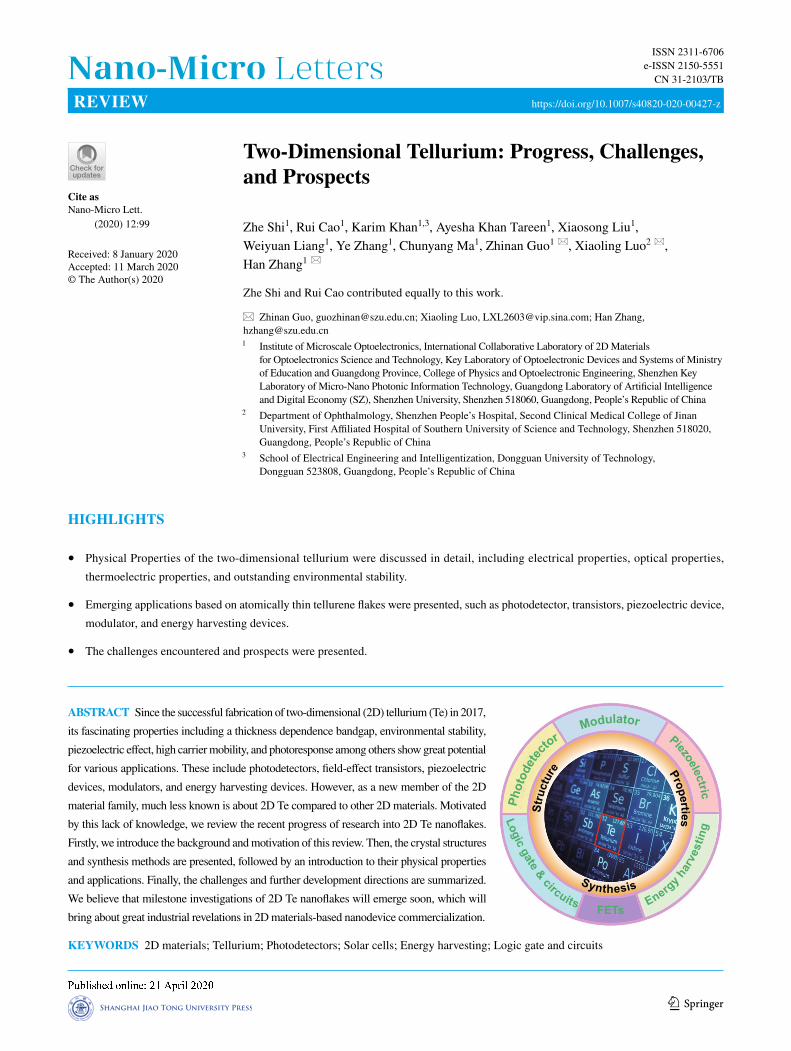
Through a combination of first‑principles calculations and experiments, Zhu et al. [63] discovered that 2D Te (a.k.a. tel‑lurene) possesses three phases, (α‑, γ‑Te) and tetragonal (β‑Te) structures, as shown in Fig. 1a–c. The formation mechanism was found to be inherently rooted in the multivalent nature of Te. The α‑ and γ‑Te phases showed a three‑ and sixfold coordi‑nation structure, respectively. However, the β‑Te phase exhib‑ited a mixture of three‑ and fourfold coordination structures; these findings suggested that Te possesses multiple bonding configurations. Subsequently, Qiao et al. [64] reported a simi‑lar investigation of the structure of few‑layer Te. The crystal structure of the α‑phase was found to consist of parallel helical Te chains with three Te atoms were included in each repeating unit. The β‑phase can be achieved by further decreasing the thickness of the α‑phase Te to a monolayer and the structure of
Nano‑Micro Lett. (2020) 12:99 Page 3 of 34 99
1 3
the β‑Te proved to be in accordance with BP. Additionally, no soft phonon modes were observed for monolayer β‑Te, and a cohesive energy of 2.567 eV atom−1 indicated that the kinetics of single‑layer β‑Te is relative more stable [24]. Notably, Te is composed of atomic chains in a triangular helix, which are stacked together via van der Waals forces in a hexagonal array and possess a 1D crystal structure rather than a layered 2D van der Waals structure (Fig. 1d). Furthermore, Te atoms form covalent bonds to only the two closest neighboring Te atoms in the helical chain (Fig. 1e), which is in sharp contrast to the structure of other traditional 2D materials like grapheme, BP, and TMDCs that possess layered structures with strong chemi‑cal bonds within the layer. When viewed along the x‑axis, the zigzag layers are seen to be stacked together via van der Waals forces to form a 3D structure (Fig. 1f) [25, 26].
2.2 Synthesis Method
For BP, high‑quality and large‑area 2D flakes are difficult to synthesize; in contrast, the 2D Te nanoflakes can be directly synthesized via multiple facile methods [65]. In this section, four commonly employed synthesis techniques to produce 2D Te are introduced, namely PVD, MBE, solution synthe‑sis, LPE, and thermal evaporation.
2.2.1 Physical Vapor Deposition
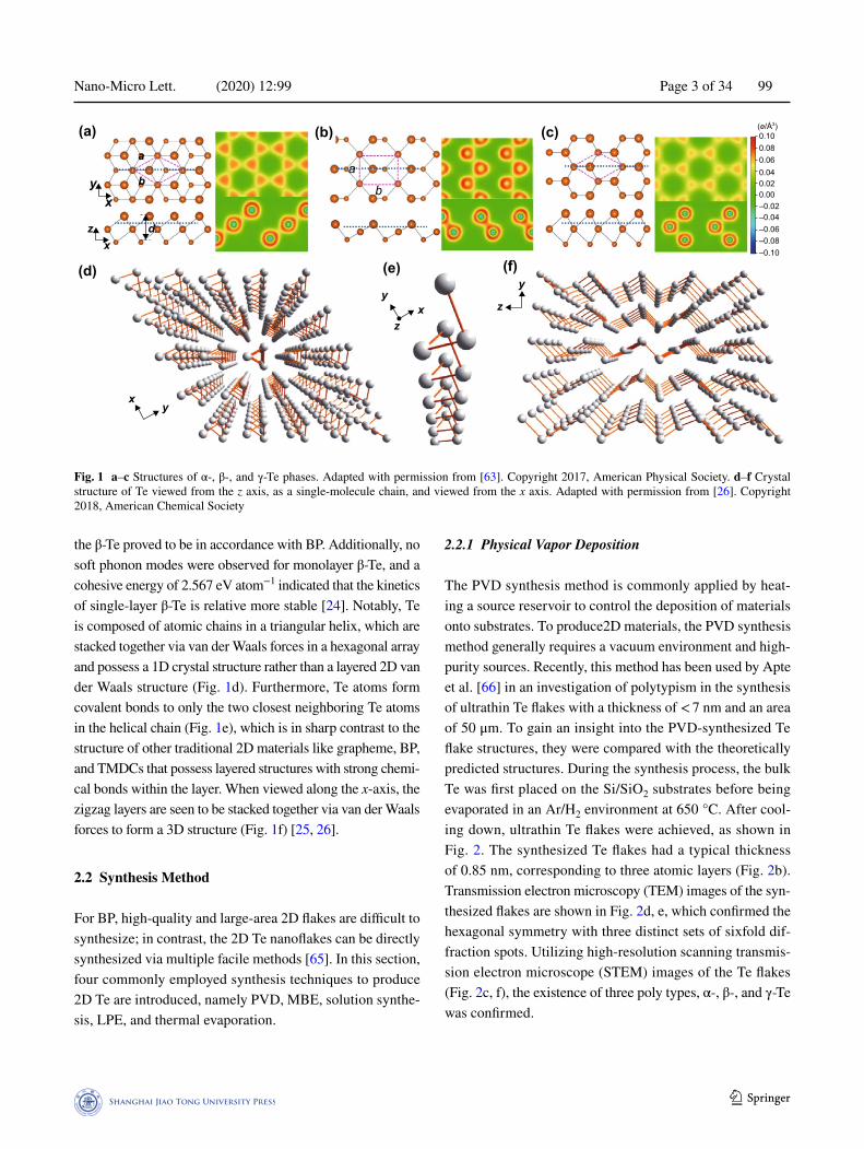
The PVD synthesis method is commonly applied by heat‑ing a source reservoir to control the deposition of materials onto substrates. To produce2D materials, the PVD synthesis method generally requires a vacuum environment and high‑purity sources. Recently, this method has been used by Apte et al. [66] in an investigation of polytypism in the synthesis of ultrathin Te flakes with a thickness of < 7 nm and an area of 50 μm. To gain an insight into the PVD‑synthesized Te flake structures, they were compared with the theoretically predicted structures. During the synthesis process, the bulk Te was first placed on the Si/SiO2 substrates before being evaporated in an Ar/H2 environment at 650 °C. After cool‑ing down, ultrathin Te flakes were achieved, as shown in Fig. 2. The synthesized Te flakes had a typical thickness of 0.85 nm, corresponding to three atomic layers (Fig. 2b). Transmission electron microscopy (TEM) images of the syn‑thesized flakes are shown in Fig. 2d, e, which confirmed the hexagonal symmetry with three distinct sets of sixfold dif‑fraction spots. Utilizing high‑resolution scanning transmis‑sion electron microscope (STEM) images of the Te flakes (Fig. 2c, f), the existence of three poly types, α‑, β‑, and γ‑Te was confirmed.
0.100.080.060.040.020.00–0.02–0.04–0.06–0.08–0.10
(e/Å3)
xy
zx
y
a
b
x
d
a
b
x
y
zz
y
(a) (b)
(d) (e) (f)
(c)
Fig. 1 a–c Structures of α‑, β‑, and γ‑Te phases. Adapted with permission from [63]. Copyright 2017, American Physical Society. d–f Crystal structure of Te viewed from the z axis, as a single‑molecule chain, and viewed from the x axis. Adapted with permission from [26]. Copyright 2018, American Chemical Society

Nano‑Micro Lett. (2020) 12:99 99 Page 4 of 34
https://doi.org/10.1007/s40820‑020‑00427‑z© The authors
2.2.2 Molecular Beam Epitaxy
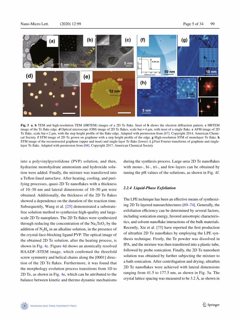
In contrast to the conventional heteroepitaxy method, the van der Waals epitaxy (vdWE) synthesis method is of great interest to produce ultrathin 2D layered materials. This syn‑thesis method can overcome the large lattice mismatch and facilitate the migration of the 2D material’s adatoms along a mica substrate surface. Additionally, the vdWE method ena‑bles over layers to be relaxed perfectly without considering the strain in the heterointerface. Recently, vdWE has been employed for the synthesis of 2D Te thin films on mica and graphene substrates [67], as shown in Fig. 3. The resulting 2D Te nanoflakes grown on the mica substrate exhibited large lateral dimensions (30–80 nm) and highly singular crystallinity, as shown in Fig. 3d, e. The chemical composi‑tion and microstructure of the Te flakes were characterized by TEM. Figure 3a–c shows the hexagonal profile of the whole sample, one corner, and an edge of the Te nanoplates, respectively. Furthermore, 2D Te flakes with mono‑ and few‑layer thicknesses were synthesized successfully on a graphene/6H‑SiC (0001) substrate, as shown in Fig. 3f–j.
Using scanning tunneling microscopy (STM) measurements, the obtained Te flakes were found to be composed of paral‑lel helical Te chains located on the surface of the graphene substrate. It can be seen from Fig. 3g, h that the lowest step height between the graphene substrate and the Te flake was approximately 0.13 nm, which confirmed that single‑layer Te flakes were achieved. The fast Fourier transform (FFT) measurement showed that the Te flakes exhibited a rectan‑gular lattice structure, which was in sharp contrast to the hexagonal symmetry of the graphene, as shown in Fig. 3i, j.
2.2.3 Solution Syntheses
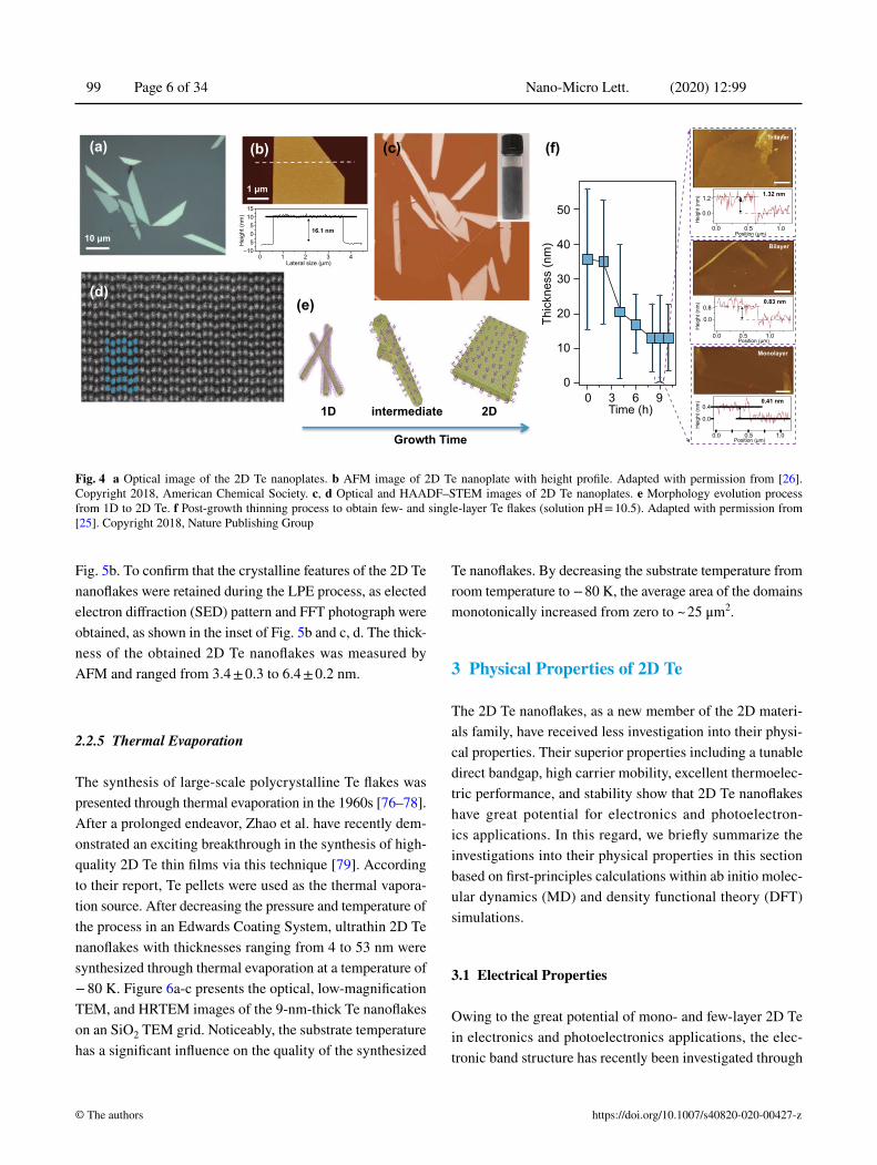
The production of 2D materials with large areas and high quality is essential for their further development in large‑scale electronic and optoelectronics applications [69, 70]. Recently, several investigations have presented the fab‑rication of large‑area and high‑quality 2D Te nanoplates based on the solution synthesis technique [25, 26]. Fig‑ure 4a, b presents solution‑synthesized environmentally stable quasi‑2D Te flakes. Firstly, Na2TeO3 was dissolved
(a) (b)
(d) (e)(f)
(c)Sio2/Si 650 °C
TeAr/H2
0.85 nm2 μm
5 nm10 nm
[0001]
50 μm
Fig. 2 Ultrathin Te flakes synthesized by PVD. a Schematic of the experimental setup. b Atomic force microscopy (AFM) image of the edge of a Te flake including a profile taken along the dotted line showing the thickness of the flake. c High‑angle annular dark‑field scanning transmis‑sion electron microscopy (HAADF–STEM) image of Te flakes showing the large‑scale uniformity. d, e TEM images of Te flakes showing their structure measured by electron diffraction (inset of d). f Atomically resolved HAADF–STEM images of the three Te polymorphs. Adapted with permission from [66]. Copyright 2019, WILEY–VCH
Nano‑Micro Lett. (2020) 12:99 Page 5 of 34 99
1 3
into a polyvinylpyrrolidone (PVP) solution, and then, hydrazine monohydrate ammonium and hydroxide solu‑tion were added. Finally, the mixture was transferred into a Teflon‑lined autoclave. After heating, cooling, and puri‑fying processes, quasi‑2D Te nanoflakes with a thickness of 10–30 nm and lateral dimensions of 10–50 μm were obtained. Additionally, the thickness of the 2D Te flakes showed a dependence on the duration of the reaction time. Subsequently, Wang et al. [25] demonstrated a substrate‑free solution method to synthesize high‑quality and large‑scale 2D Te nanoplates. The 2D Te flakes were synthesized through reducing the concentration of the Na2TeO3 by the addition of N2H4 in an alkaline solution, in the presence of the crystal‑face‑blocking ligand PVP. The optical image of the obtained 2D Te solution, after the heating process, is shown in Fig. 4c. Figure 4d shows an atomically resolved HAADF–STEM image, which confirmed the threefold screw symmetry and helical chains along the [0001] direc‑tion of the 2D Te flakes. Furthermore, it was found that the morphology evolution process transitions from 1D to 2D Te, as shown in Fig. 4e, which can be attributed to the balance between kinetic and thermo dynamic mechanisms
during the synthesis process. Large‑area 2D Te nanoflakes with mono‑, bi‑, tri‑, and few‑layers can be obtained by tuning the pH values of the solutions, as shown in Fig. 4f.
2.2.4 Liquid‑Phase Exfoliation
The LPE technique has been an effective means of synthesiz‑ing 2D Te layered nanoarchitectures [69–74]. Generally, the exfoliation efficiency can be determined by several factors, including sonication energy, favored anisotropic characteris‑tics, and solvent‑nanoflake interactions of the bulk materials. Recently, Xie et al. [75] have reported the first production of ultrathin 2D Te nanoflakes by employing the LPE syn‑thesis technique. Firstly, the Te powder was dissolved in IPA, and the mixture was then transferred into a plastic tube, followed by probe sonication. Finally, the 2D Te nanosheet solution was obtained by further subjecting the mixture to a bath sonication. After centrifugation and drying, ultrathin 2D Te nanoflakes were achieved with lateral dimensions ranging from 41.5 to 177.5 nm, as shown in Fig. 5a. The crystal lattice spacing was measured to be 3.2 Å, as shown in
(a) (b) (c) (f) (g)
(d) (e)(h)
50 nm 10 nm
i
j5 nm
5 nm
32 nm
5 nm120°
3.8 Å
(100)(10
0)
(110)
50 μm
5 nm 0.39 nm0.4
0.2
0.0
0 5 10 15 20
(100)
2 μm
Distance (nm)
Hig
ht (n
m)
bc
(110)
Fig. 3 a, b TEM and high‑resolution TEM (HRTEM) images of a 2D Te flake. Inset of b shows the electron diffraction pattern. c HRTEM image of the Te flake edge. d Optical microscope (OM) image of 2D Te flakes, scale bar = 4 μm, with inset of a single flake. e AFM image of 2D Te flake, scale bar = 2 μm, with the step height profile of the flake edge. Adapted with permission from [67]. Copyright 2014, American Chemi‑cal Society. f STM image of 2D Te grown on graphene with a step height profile of the edge. g High‑resolution STM of monolayer Te flake. h STM image of the reconstructed graphene (upper and inset) and single‑layer Te flake (lower). i, j Fast Fourier transforms of graphene and single‑layer Te flake. Adapted with permission from [68]. Copyright 2017, American Chemical Society
Nano‑Micro Lett. (2020) 12:99 99 Page 6 of 34
https://doi.org/10.1007/s40820‑020‑00427‑z© The authors
Fig. 5b. To confirm that the crystalline features of the 2D Te nanoflakes were retained during the LPE process, as elected electron diffraction (SED) pattern and FFT photograph were obtained, as shown in the inset of Fig. 5b and c, d. The thick‑ness of the obtained 2D Te nanoflakes was measured by AFM and ranged from 3.4 ± 0.3 to 6.4 ± 0.2 nm.
2.2.5 Thermal Evaporation
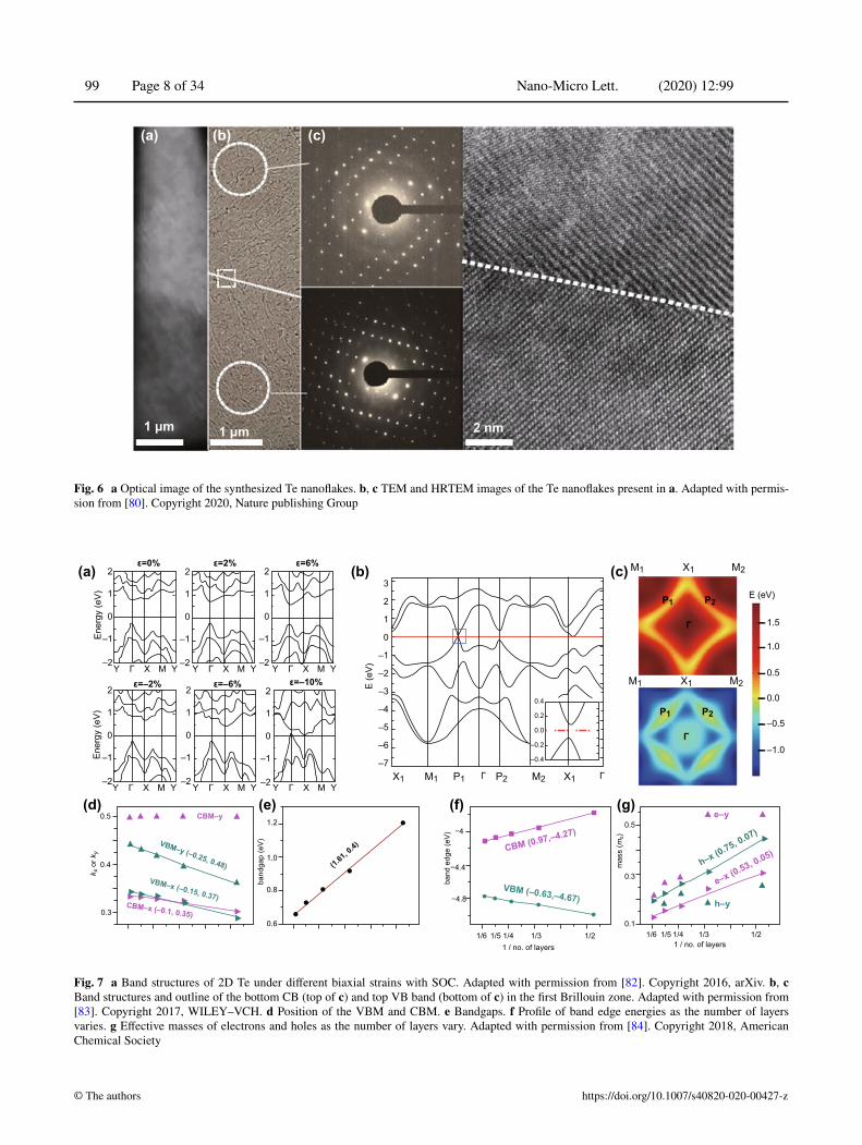
The synthesis of large‑scale polycrystalline Te flakes was presented through thermal evaporation in the 1960s [76–78]. After a prolonged endeavor, Zhao et al. have recently dem‑onstrated an exciting breakthrough in the synthesis of high‑quality 2D Te thin films via this technique [79]. According to their report, Te pellets were used as the thermal vapora‑tion source. After decreasing the pressure and temperature of the process in an Edwards Coating System, ultrathin 2D Te nanoflakes with thicknesses ranging from 4 to 53 nm were synthesized through thermal evaporation at a temperature of − 80 K. Figure 6a‑c presents the optical, low‑magnification TEM, and HRTEM images of the 9‑nm‑thick Te nanoflakes on an SiO2 TEM grid. Noticeably, the substrate temperature has a significant influence on the quality of the synthesized
Te nanoflakes. By decreasing the substrate temperature from room temperature to − 80 K, the average area of the domains monotonically increased from zero to ~ 25 μm2.
3 Physical Properties of 2D Te
The 2D Te nanoflakes, as a new member of the 2D materi‑als family, have received less investigation into their physi‑cal properties. Their superior properties including a tunable direct bandgap, high carrier mobility, excellent thermoelec‑tric performance, and stability show that 2D Te nanoflakes have great potential for electronics and photoelectron‑ics applications. In this regard, we briefly summarize the investigations into their physical properties in this section based on first‑principles calculations within ab initio molec‑ular dynamics (MD) and density functional theory (DFT) simulations.
3.1 Electrical Properties
Owing to the great potential of mono‑ and few‑layer 2D Te in electronics and photoelectronics applications, the elec‑tronic band structure has recently been investigated through
Time (h)0
0
10
20
30
40
50
3 6 9
Hei
ght (
nm)
Position (µm)0.0 0.5 1.0
0.4
0.0
0.41 nm
0.83 nm
Monolayer
Hei
ght (
nm)
Position (µm)0.0 0.5 1.0
0.8
0.0
0.0
0.0
1.2
0.5 1.0
1.32 nm
Position (µm)
Hei
ght (
nm)
Bilayer
Trilayer
(c)(b)(a)
(e)
(f)
16.1 nm
1510505
–100 1 2 3 4
Hei
ght (
nm)
1 μm
10 μm
D2D1
Growth Time
(d)
Thic
knes
s (n
m)
intermediate
Fig. 4 a Optical image of the 2D Te nanoplates. b AFM image of 2D Te nanoplate with height profile. Adapted with permission from [26]. Copyright 2018, American Chemical Society. c, d Optical and HAADF–STEM images of 2D Te nanoplates. e Morphology evolution process from 1D to 2D Te. f Post‑growth thinning process to obtain few‑ and single‑layer Te flakes (solution pH = 10.5). Adapted with permission from [25]. Copyright 2018, Nature Publishing Group

Nano‑Micro Lett. (2020) 12:99 Page 7 of 34 99
1 3
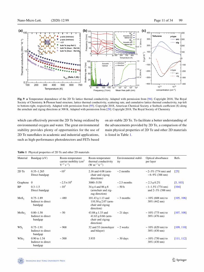
various theoretical calculations, including first‑principles calculations based on DFT and ab initio MD simulations [81]. Zhu et al. [82] reported that monolayer 2D Te pos‑sesses a direct bandgap of 1.04 eV by using first‑principles calculations. Additionally, by introducing an external strain, both the transport properties and the bandgap can be tuned, as shown in Fig. 7a. As the tensile strain was increased from 0 to 6%, the conduction band minimum (CBM) showed a gradual downshift behavior toward the Fermi level. In con‑trast, the valence band maximum (VBM) barely changed. Consequently, the bandgap decreased to 0.86 eV for 6% tensile strain. Xian et al. [83] presented results by first‑principles calculations suggesting that 2D Te possessed a chair‑like buckled structure rather than a hexagonal struc‑ture. Owing to this special structure, the 2D Te caused ani‑sotropic band dispersions around the Fermi level, which
can be explained via a generalized semi‑Dirac Hamilto‑nian. The calculated band structure, as well as the spin–orbit coupling (SOC) of 2D Te, is shown in Fig. 7b, c. It can be seen clearly in Fig. 7a that Dirac‑cone‑like dispersions occurred at P1 in the Brillouin zone (BZ). Furthermore, in contrast to the dispersions of the group‑IV 2D materials, these dispersions showed highly anisotropic behavior, as shown in Fig. 7c. Recently, Liu et al. [84] have presented work with first‑principles calculations showing that along different transport directions, the isotropy of the few‑layer 2D Te is related to the potential and effective mass of the charge carriers, as shown in Fig. 7d–g. More importantly, the calculated bandgaps increased as the thickness of the few‑layer 2D Te decreased. The band edge energies also showed similar behavior, varying linearly with 1/n or 1/d (where n and d denote the layer number and thickness of the 2D Te
–2.2 nm
200.0 nm
4.2 nm
1
32
0.32 nm
ca.6.88 nm ca.6.20 nm ca.6.18 nm
ca.5.12 nm
0 20 40 60 80 100 120 140
0
0 30 60 90 120 150 180
50 100 150 200 250 300
ca.3.42 nmca.3.45 nm
Horizontal Distance (nm)
43210
–1
–1012345
543210
–1–2
678
(b)(a)
(c)
200 nm
(d)
Fig. 5 a, b TEM and HRTEM images of the 2D Te nanoflakes. Insets of b: SED pattern and FFT photograph of the 2D Te nanoflakes (top and bottom). c AFM image of the ultrathin 2D Te nanoflakes. d Height profiles of the 2D Te nanoflakes presented in part c. Adapted with permission from [75]. Copyright 2018, WILEY–VCH
Nano‑Micro Lett. (2020) 12:99 99 Page 8 of 34
https://doi.org/10.1007/s40820‑020‑00427‑z© The authors
1 μm 1 μm 2 nm
(a) (b) (c)
Fig. 6 a Optical image of the synthesized Te nanoflakes. b, c TEM and HRTEM images of the Te nanoflakes present in a. Adapted with permis‑sion from [80]. Copyright 2020, Nature publishing Group
0.4
0.2
0.0
–0.2
–0.4
CBM (0.97,–4.27)
VBM (–0.63,–4.67)
h–x (0.75, 0.07)
e–x (0.53, 0.05)
h–y
e–y0.5
0.3(1.
61, 0
.4)VBM–y (–0.25, 0.48)
VBM–x (–0.15, 0.37)CBM–x (–0.1, 0.35)
CBM–y
1/6 1/5 1/4 1/3 1/6 1/5 1/4 1/31/2 1/21 / no. of layers 1 / no. of layers
0.1
mas
s (m
0)
(g)
band
edg
e (e
V)
(f)−4
−4.4
−4.8
1.2
1.0
0.8
0.6
band
gap
(eV)
0.5
0.4
0.3
k x o
r ky
2
1
0
–1
–2
2
1
0
–1
–2
2
1
0
–1
–2
2
1
0
–1
–2
2
1
0
–1
–2
2
1
0
–1
–2
–7
–6
–5
–4
–3
–2
–1
0
1
2
3
Ener
gy (e
V)En
ergy
(eV)
E (e
V)
E (eV)
M2X1M1
M2X1 X1M1 P1 P2
M2X1M1
P1 P2
1.5
1.0
0.5
0.0
–0.5
–1.0
Γ
P1 P2
Γ
ΓΓ
(c)(b)(a)
(e)(d)Y Γ X M Y Y Γ X M Y Y Γ X M Y
Y Γ X M YY Γ X M YY Γ X M Yε=–10%ε=–6%ε=–2%
ε=6%ε=2%ε=0%
Fig. 7 a Band structures of 2D Te under different biaxial strains with SOC. Adapted with permission from [82]. Copyright 2016, arXiv. b, c Band structures and outline of the bottom CB (top of c) and top VB band (bottom of c) in the first Brillouin zone. Adapted with permission from [83]. Copyright 2017, WILEY–VCH. d Position of the VBM and CBM. e Bandgaps. f Profile of band edge energies as the number of layers varies. g Effective masses of electrons and holes as the number of layers vary. Adapted with permission from [84]. Copyright 2018, American Chemical Society

Nano‑Micro Lett. (2020) 12:99 Page 9 of 34 99
1 3
nanoflakes, respectively), as shown in Fig. 7f. Additionally, the effective mass of charge carriers being transported across the chains increased linearly with 1/n or 1/d. These findings enable the evaluation of the electronic properties of 2D Te at different thicknesses.
3.2 Optical Properties
Optical properties are another important parameter for electronics and photoelectronics applications of 2D Te, in particular for photodetectors and FET devices [85, 86]. Recently, investigations have been carried out to gain a bet‑ter insight into the optical properties of 2D Te. Firstly, Wu et al. [24] reported strong light absorption in few‑layer β‑Te from the ultraviolet (UV) band to the visible band, as shown
in Fig. 8a. For the few‑layer β‑Te, the calculated optical absorption coefficients showed clear layer‑dependent behav‑ior, in which the absorption coefficients decreased as the thickness of the few‑layer β‑Te increased. This was attributed to the thickness‑dependent band dispersion and interlayer electronic hybridization; both processes were enhanced with increasing thickness. These outcomes showed that few‑layer β‑Te is a promising material for acousto‑optic and UV–vis‑ible deflectors. As previously mentioned, 2D Te can be syn‑thesized with large areas, which enables high‑performance FETs and photodetectors based on 2D Te. Recently, Wang et al. [25] have reported an investigation on FETs based on large‑scale 2D Te. In their report, thickness‑ and angle‑dependent Raman spectra were employed to characterize the optical properties of 2D Te at room temperature, as shown
Wavelength (nm)
0 300 600 900 1200 1500 18000.5
1.0
1.5
2.0
2.5
3.0 (c)(b)(a)monolayer
bilayer
trilayerbulk β−Te
Abso
rptio
n co
effic
iem
(1E5
cm
−1)
Inte
nsity
(a.u
.)
Inte
nsity
(a.u
.)
80 100 120 140 160
13.5 nm thickness94 105 125 143
cm−1 cm−1 cm−1 cm−1
2L3L4L5L6LBulk
9.0
6.0
3.0
0.0
Energy of incident light (eV)0.8 1.6 2.4 3.2 4.00.8 1.6 2.4 3.2 4.0
Energy of incident light (eV) Energy of incident light (eV)
Raman shift (cm−1) Raman shift (cm−1)80 100 120 140 160
Abso
rban
ce (%
) 6.09.0
6.0
3.0
0.0
4.0
2.0
0.0
(f)(e)(d)6L−x6L−y6L−z
2L−x2L−y2L−z
z
y
0.8 1.6 2.4 3.2 4.0
37.4 nm
30.2 nm
27.9 nm
20.5 nm
14.3 nm
12.8 nm
9.1 nm
5.7 nm
4.1 nm
2.4 nm
TriLayer
Bilayer
Ei-TO
Ei-LO
A1
E2
180°
150°
120°
90°
60°
30°
0°
Fig. 8 Optical properties of 2D Te. a Absorption coefficients of the bulk, few‑layer, and monolayer β‑Te. Adapted with permission from [24]. Copyright 2017, IOP Publishing. b, c Raman and angle‑resolved Raman spectra of the 2D Te flakes. Adapted with permission from [25]. Copy‑right 2018, Nature Publishing Group. d, e Absorbance of 2 layer and 6‑layer α‑Te with the incident light polarization along the x‑, y‑, and z‑direction. f Absorbance of incident light polarized in the direction for few‑layer α‑ and bulk Te. Adapted with permission from [64]. Copyright 2018, Elsevier

Nano‑Micro Lett. (2020) 12:99 99 Page 10 of 34
https://doi.org/10.1007/s40820‑020‑00427‑z© The authors
in Fig. 8b, c. Three Raman active modes were observed as the thickness of the 2D Te was varied from a monolayer to 37.4 nm. Additionally, for a moderate thickness of the 2D Te flakes (less than 20.5 nm), three different Raman active modes located at approximately 92, 121, and 125 cm−1 were found, which is consistent with previous investigations. These findings suggested that the symmetric characteris‑tics of the bulk Te were appropriate for its 2D morphology. Further decreasing the thickness to 9.1 nm, the E1 longitu‑dinal (LO) mode appeared, and this can be attributed to the enhanced deformation potential and the weakened electro‑optic effect in the 2D Te lattice. As the thickness of the 2D Te samples continued to decrease (less than 9.1 nm), degeneracy in the E1 transverse (TO) and LO modes was observed with peak broadening, this may be caused by the symmetry assignments, electronic band structure changes, and thickness‑dependent intra‑chain atomic displacement for each band. Meanwhile, due to the unique chiral‑chain structure, significant peak shifts were found in the Raman spectra as the thickness varied. Broadband absorption and strong light absorption of few‑layer α‑Te were investigated by Qiao et al. [64]. The calculated absorbances at 1.6 and 3.2 eV were 2–3% and 6–9% per layer (Fig. 8d, e), respec‑tively, two to three times larger than that of BP. The excellent optical absorbances indicated the promising potential of the few‑layer α‑Te for broadband optical applications ranging from the visible band to the infrared band. Furthermore, the absorbance showed layer‑dependent behavior (Fig. 8f), where the absorption efficiency increased as the sample thickness was reduced. The strong interchain and interlayer couplings in the few‑layer α‑Te are two key processes that enhance the absorbance significantly. For two incident light sources with wavelengths of 512 and 382 nm, the absorb‑ance of per layer for bilayer α‑Te is nearly 1.65 and 2 times higher than that of bulk Te, respectively.
3.3 Thermoelectric Properties
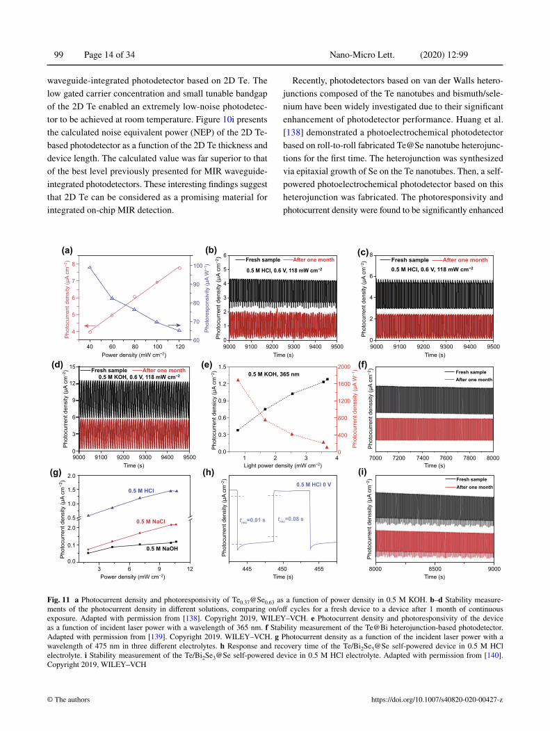
With the increasing global consumption of energy and the shortage of fossil fuel resources, it is of great significance to harvest waste heat energy. Thermoelectric technology provides an effective way to convert the waste heat into useful electricity on a large scale. Since the discovery of 2D materials, they have attracted considerable attention for thermoelectric applications. However, compared to
the well‑studied thermoelectric properties of the other 2D materials, including graphene, monoelemental borophene [87], germanene [88–90], silicene [88, 91], and arsenene [92, 93], the thermoelectric properties of 2D Te nanoflakes have received relatively little attention. In this section, we highlight some representative investigations into the thermoelectric properties of 2D Te nanoflakes. Gao et al. [94] investigated the thermal properties of 2D Te flakes theoretically by applying first‑principles calculations and phonon Boltzmann transport, as shown in Fig. 9a. Accord‑ing to the calculated results, 2D Te possesses an extremely low room‑temperature lattice thermal conductivity (KL) of only 2.16 and 4.08 W m−1 K−1 along the armchair and zigzag directions, respectively, which are comparable to that of bulk Te. More importantly, compared to the other 2D materials, the calculated KL of the 2D Te was the low‑est, and this can be attributed to the ultra‑low‑energy opti‑cal modes, soft acoustic modes, and intensive scattering of optical‑acoustic phonons. Subsequently, Sharma et al. investigated the thermoelectric properties of the 2D Te by combining first‑principles calculations with semi‑classical Boltzmann transport theory. The 2D Te was found to pos‑sess the lowest KL compared to the other monoelemental 2D materials (Fig. 9b) [95]. This was attributed to the intensive scattering of acoustic phonons into optical pho‑nons. Lin et al. [29] explored the thermoelectric properties of single‑layer 2D Te using DFT calculations. Similar to the previous investigations, the anharmonic scattering pro‑cess dominated and effectively limited its lattice thermal conductivity. Consequently, the calculated KL represented the lowest value among the previously investigated monoe‑lemental 2D materials (Fig. 9c).
3.4 Stability
The environmental stability is another important property of 2D materials. For many 2D materials, such as BP [19, 21, 96–98] and TMDCs [99–102], instability has severely hindered their further development in both academic and industrial applications. In sharp contrast, extraordinary environmental stability has been demonstrated for vari‑ous thicknesses of 2D Te (ranging from few‑layer to mon‑olayer). The superior environmental stability is mainly due to existence of an energy barrier in the oxidation pathways,
Nano‑Micro Lett. (2020) 12:99 Page 11 of 34 99
1 3
which can effectively prevent the 2D Te being oxidized by environmental oxygen and water. The great environmental stability provides plenty of opportunities for the use of 2D Te nanoflakes in academic and industrial applications, such as high‑performance photodetectors and FETs based
on air‑stable 2D Te. To facilitate a better understanding of the advancements provided by 2D Te, a comparison of the main physical properties of 2D Te and other 2D materials is listed in Table 1.
a
by
z
x
x
bulk Te (exp Ref.1)bulk Te (theor⊥Ref.34)bulk Te (theor⊥Ref.34)
~1/Ty-axis (intrinsic)y-axis (intrinsic) Tellurene
arczig
400
300
200
100
0
400
300
200
100
0
−100
−200
−300
−400
−100
−200
−300
−400
arczig
p-type
n-type
kxx1
kxx1
Acoustie (xx)Optical (xx)
Acoustic (yy)Optical (yy)
MYΓX0
50
100
150
200 1.5
1.0
0.5
0300 500 700 900Temperature (K)
k1 (W/m
K)
1.5
1.0
0.5
0.0
k1 (W/m
K)
101310310210110010−1 1014
concentration (cm−2)Temperature (K)Frequency (1/cm)
Freq
uenc
y (1
/cm
)
Mean free path (nm)
S (μ
V K−1
)
0 50 100 150
100
75
50
25
0700600500400300200100Sc
atte
ring
rate
(1/p
s)
kmin (Refs.1,35)
AcousticOptical
x−directiony−direction
0.2
1
10
100(c)(b)(a)
Ther
mal
con
duct
ivity
(Wm
−1 K
−1)
c
Fig. 9 a Temperature dependence of the 2D Te lattice thermal conductivity. Adapted with permission from [94]. Copyright 2018, The Royal Society of Chemistry. b Phonon band structure, lattice thermal conductivity, scattering rate, and cumulative lattice thermal conductivity, top‑left to bottom‑right, respectively. Adapted with permission from [95]. Copyright 2018, American Chemical Society. c Seebeck coefficient (S) along the armchair and zigzag directions at 300 K. Adapted with permission from [29]. Copyright 2018, The Royal Society of Chemistry
Table 1 Physical properties of 2D Te and other 2D materials
Material Bandgap (eV) Room‑temperature carrier mobility (cm2 V−1 s−1)
Room‑temperature thermal conductivity (W m−1 k−1)
Environmental stabil‑ity
Optical absorbance per layer
Refs.
2D Te 0.35–1.265Direct bandgap
~103 2.16 and 4.08 (arm‑chair and zigzag directions)
~ 2 months ~ 2–3% (774 nm) and ~ 6–9% (388 nm)
[25]
Graphene 0 ~ 2.5 × 10⁴ 3080–5150 ~ 2.5 months ~ 2.3 ± 0.2% [5, 103]BP 0.3–1.5
Direct bandgap~ 103 34 ± 4 and 86 ± 8
(armchair and zig‑zag direction)
~ 50 h ~ 1–1.5% (774 nm) and 2–3% (388 nm)
[104]
MoS2 0.75–1.89Indirect to direct
bandgap
~ 480 101.43 ± 1.13 and 110.30 ± 2.07 (arm‑chair and zigzag direction)
~ 3 months ~ 10% (688 nm) to 30% (442 nm)
[105, 106]
MoSe2 0.80–1.58Indirect to direct
bandgap
~ 50 43.88 ± 1.33 and 41.63 ± 0.66 (arm‑chair and zigzag direction)
~ 21 days ~ 10% (775 nm) to 30% (476 nm)
[107, 108]
WS2 0.75–1.91Indirect to direct
bandgap
~ 968 32 and 53 (monolayer and bilayer)
~ 2 weeks ~ 10% (620 nm) to 30% (430 nm)
[109, 110]
WSe2 0.90 to 1.54Indirect to direct
bandgap
~ 500 3.935 ~ 30 days ~ 10% (750 nm) to 30% (430 nm)
[111, 112]

Nano‑Micro Lett. (2020) 12:99 99 Page 12 of 34
https://doi.org/10.1007/s40820‑020‑00427‑z© The authors
4 Applications
Owing to the unique helical chain structure, excellent envi‑ronmental stability, high carrier mobility, and low‑cost syn‑thesis methods of 2D Te nanoflakes, it holds great potential for high‑performance 2D material‑based electronic and pho‑toelectronic devices. In this section, we summarize some recent representative progress in the applications of 2D Te nanoflakes.
4.1 Photodetector
A photodetector is a device that converts light signals into electrical signals, which is crucial in many fundamental research and practical applications. The strong light‑matter interaction, large‑scale, and environmental stability of 2D Te nanoflakes make them a promising candidate material for high‑performance photodetector applications. In general, the mechanisms of photocurrent generation in 2D Te nanoflakes are photovoltaic, photobolometric, photogating, and photo‑thermoelectric effects [113–115]. The metrics employed to characterize the performance of a photodetector include the specific detectivity, response spectrum range, response time, external quantum efficiency, photogain, noise equivalent power, and photoresponsivity. Here, we discuss the perfor‑mance of a photodetector based on 2D Te nanoflakes with free‑space and waveguide configurations using the metrics.
Three of the most well‑known and intensively investi‑gated 2D materials are BP [116–120], TMDCs [121–131], and graphene [132–136] due to their superior properties and strong light‑matter interactions. As a new member of the 2D materials family, 2D Te has received less attention than the aforementioned three sorts of 2D materials. How‑ever, the excellent environmental stability, simple synthesis, high quality, and large achievable scale of 2D Te nanoflakes have recently motivated a surge of academic interest. Subse‑quently, experiment results have indicated its suitability for high‑performance photodetectors. For example, Wang et al. reported a high‑photoresponsivity, flexible photodetector based on vdWE‑synthesized hexagonal 2D Te nanoplates on a flexible mica substrate [25].The fabricated photodetector exhibited excellent stability and photoresponsivity, as shown in Fig. 10a. The measured current under illumination pre‑sented the same level of both noise and photocurrent, and the
corresponding photoresponsivity was approximately 162.4 A W−1, indicating the high stability and photoresponsivity of the 2D Te‑based photodetector. More importantly, the meas‑ured photocurrent and noise current only changed slightly after the device was subjected to100 continuous bending cycles (Fig. 10b, c), which proved the device is suitable for wearable and flexible optoelectronic device applications. Subsequently, Amani et al. [26] demonstrated short‑wave infrared photodetectors based on solution‑synthesized, envi‑ronmentally stable quasi‑2D Te nanofilms. An Au/Al2O3 optical cavity substrate was employed to further enhance the absorption of the device. Additionally, by adjusting the Al2O3 spacer thickness, the peak photoresponsivity wave‑length of the device can be tuned from 1.4 μm (13 A W−1) to 2.4 μm (8 A W−1), with nonzero photoresponsivity up to 3.4 μm, as shown in Fig. 10d [26]. In order to further characterize the performance of the fabricated photodetector, the responsivity as a function of various laser wavelengths was measured for device temperatures of 78 and 297 K (Fig. 10e). The responsivity peaked at λ = 1.7 μm with values of 27 A W−1 (at 78 K) and 16 A W−1 (at 297 K). The cor‑responding calculated specific detectivity at 78 and 297 K were 2.6 × 10¹¹ and 2.9 × 10⁹, respectively (Fig. 10f). The enhancement of the specific detectivity at 78 K was due to more efficient suppression of the noise current than at room temperature, which was inversely proportional to the specific detectivity. These outcomes proved that the solution‑synthe‑sized 2D Te nanoflakes were suitable for high‑performance photodetectors covering the whole near infrared (IR) band. Recently, Xie et al. have demonstrated a high photoresponse photodetector based on LPE‑synthesized 2D non‑layered Te nanosheets [75]. Photoelectrochemical measurements were taken to evaluate the photoresponse of the fabricated pho‑todetector. In contrast to the previous investigations, this study mainly focused on the photoresponse of the device from the UV to visible bands. At a fixed bias voltage and KOH solution concentration, measurements of photocurrent and photoresponse as a function of incident laser power at different wavelengths were carried out, as shown in Fig. 10g, h, respectively. The measured photocurrent was signifi‑cantly enhanced by increasing the incident laser power for the five different wavelengths employed in the experiment. Consequently, the photoresponse, which is proportional to the photocurrent, was strengthened as well. Meanwhile, the stability and KOH solution concentration dependence

Nano‑Micro Lett. (2020) 12:99 Page 13 of 34 99
1 3
measurements were also taken, and the outcomes indicated that the LPE‑synthesized 2D non‑layered Te nanosheet is a promising material for photodetectors in the UV to vis‑ible bands as well as other photoelectric applications. Due to the small and tunable bandgap of the 2D Te nanoplates, it is a potential material for mid‑IR (MIR) photodetector applications. Compared to a free‑space detector, waveguide
integration can significantly improve the signal‑to‑noise ratio. The optical absorption behavior was found to be pro‑portional to the path length of the waveguide. Moreover, the detectable bandwidth for waveguide‑integrated photodetec‑tors was wider than that of free‑space photodetectors, mainly due to the reduced carrier transit time and RC delay. In this regard, Deckoff‑Jones et al. [137] have recently reported a
bias=0.6 V 350 nm365 nm380 nm400 nm475 nm
350 nm365 nm380 nm400 nm475 nm
Detector Length (μm)
10 nm20 nm30 nm40 nm50 nm60 nm70 nm80 nm
78 K297 K
After bending 100 times
Time (s)Time (s)Time (s)
12
11
10
9
8
7
13
12
11
10
9
Cur
rent
(μA)
Cur
rent
(μA)
Cur
rent
(μA)
Before bending
50 100 150 200 250 300500 40 80 120 160 200 240 280 320 100 150 200 250 300
2.0
1.8
1.6
1.4
1.2
1.0
off
on
λ=473 nm P=761.9 W m−2
Res
pons
ivity
(AW
)
Res
pons
ivity
(AW
)
14 1012
1011
1010
109
108
12
10
8
6
4
2
01.0 1.5 2.0 2.5 3.0 3.5 4.0 1.0 1.5 2.0 2.5
Wavelength (μm) Wavelength (μm) Wavelength (μm)
Spec
ific
Det
ectiv
ity (c
m H
z1/2 W
−1) 30
20
10
0
1.0 1.5 2.0 2.5 3.0 3.5
Vd=5 VVd=5 V
Vd=5 V16−20 nm Te
550 nm Al2O3150 nm Al2O3350 nm Al2O3
77 K293 K
4.0×10⁻²
3.0×10⁻²
2.0×10⁻²
1.0×10⁻²
Phot
ocur
rent
den
sity
(μA
cm−2
)
0.00.0 4.0×10⁻³ 8.0×10⁻³
Pλ (W cm−2)0.0 4.0×10⁻³ 8.0×10⁻³
Pλ (W cm−2)
16
14
12
10
8
6
4
2
0
Rph
(μA
W−1
)
NEP
(fW H
z1/2 )
bias=0.6 V
0.1
1
0 5 10 15
(a) (b) (c)
(d) (e) (f)
(h)(g) (i)
Fig. 10 a Photoresponse of the 2D Te‑based device as a function of time at a bias voltage of 2 V as the laser is switched on and off. b, c Pho‑toresponse as a function of time while switching the laser on and off, before and after bending the device 100 times, respectively. Adapted with permission from [67]. Copyright 2014, American Chemical Society. d Responsivities of devices fabricated on optical cavities with different Al2O3 thicknesses. e Spectral responsivity of a Te photoconductor at 78 and 297 K under a gate bias of Vd = 5 V. f Specific detectivity of Te photoconductors with optimized thickness. Adapted with permission from [26]. Copyright 2018, American Chemical Society. g, h Photocurrent and photoresponse as a function of incident power Pλ for a range of wavelengths. Adapted with permission from [75]. Copyright 2018, Wiley. i Calculated NEP of the detector as a function of the 2D Te thickness and device length. Adapted with permission from [137]. Copyright 2019, American Chemical Society
Nano‑Micro Lett. (2020) 12:99 99 Page 14 of 34
https://doi.org/10.1007/s40820‑020‑00427‑z© The authors
waveguide‑integrated photodetector based on 2D Te. The low gated carrier concentration and small tunable bandgap of the 2D Te enabled an extremely low‑noise photodetec‑tor to be achieved at room temperature. Figure 10i presents the calculated noise equivalent power (NEP) of the 2D Te‑based photodetector as a function of the 2D Te thickness and device length. The calculated value was far superior to that of the best level previously presented for MIR waveguide‑integrated photodetectors. These interesting findings suggest that 2D Te can be considered as a promising material for integrated on‑chip MIR detection.
Recently, photodetectors based on van der Walls hetero‑junctions composed of the Te nanotubes and bismuth/sele‑nium have been widely investigated due to their significant enhancement of photodetector performance. Huang et al. [138] demonstrated a photoelectrochemical photodetector based on roll‑to‑roll fabricated Te@Se nanotube heterojunc‑tions for the first time. The heterojunction was synthesized via epitaxial growth of Se on the Te nanotubes. Then, a self‑powered photoelectrochemical photodetector based on this heterojunction was fabricated. The photoresponsivity and photocurrent density were found to be significantly enhanced
60
70
80
90
1008
7
6
5
4 Phot
ores
pons
ivity
(μA
W−1
)
Pho
tocu
rren
t den
sity
(μA
cm−2
)Ph
otoc
urre
nt d
ensi
cy (μ
A cm
−2)
Phot
ocur
rent
den
sity
(μA
cm−2
)
Phot
ocur
rent
den
sity
(μA
cm−2
)Ph
otoc
urre
nt d
ensi
ty (μ
A cm
−2)
Phot
ocur
rent
den
sity
(μA
cm−2
)
Phot
ocur
rent
den
sity
(μA
cm−2
)
40 60 80 100 120
6
5
4
3
2
8
6
4
2
0
1
09000 9100 9200 9300 9400 9500
Power density (mW cm−2) Time (s)
Fresh sample After one month
0.5 M HCI, 0.6 V, 118 mW cm−2
9000 9100 9200 9300 9400 9500Time (s)
Fresh sample After one month0.5 M KOH, 0.6 V, 118 mW cm−2
Fresh sample After one month0.5 M HCI, 0.6 V, 118 mW cm−2
Fresh sampleAfter one month
Fresh sampleAfter one month
Time (s)7000 7200 7400 7600 7800 8000
Phot
ocur
rent
den
ssity
(μA
cm−2
)Ph
otoc
urre
nt d
enss
ity (μ
A cm
−2)
Phot
ocur
rent
den
ssity
(μA
W−1
)
0.5 M KOH, 365 nm1.5
1.2
0.9
0.6
0.3
0.0
Light power density (mW cm−2)
Power density (mW cm−2)
1 2 3 4
2000
1600
1200
800
400
0
tres=0.01 s trec=0.08 s
0.5 M HCl 0 V
445 450 455Time (s)
3 6 9 12
0.5 M HCl
0.5 M NaCl
0.5 M NaOH
2.0
1.5
1.0
0.5
2.0
0.1
0.0
9000 9100 9200 9300 9400 9500Time (s)
15
12
9
6
3
0
8000 8500 9000Time (s)
(a) (b) (c)
(f)(e)(d)
(g) (h) (i)
Fig. 11 a Photocurrent density and photoresponsivity of [email protected] as a function of power density in 0.5 M KOH. b–d Stability measure‑ments of the photocurrent density in different solutions, comparing on/off cycles for a fresh device to a device after 1 month of continuous exposure. Adapted with permission from [138]. Copyright 2019, WILEY–VCH. e Photocurrent density and photoresponsivity of the device as a function of incident laser power with a wavelength of 365 nm. f Stability measurement of the Te@Bi heterojunction‑based photodetector. Adapted with permission from [139]. Copyright 2019. WILEY–VCH. g Photocurrent density as a function of the incident laser power with a wavelength of 475 nm in three different electrolytes. h Response and recovery time of the Te/Bi2Se3@Se self‑powered device in 0.5 M HCl electrolyte. i Stability measurement of the Te/Bi2Se3@Se self‑powered device in 0.5 M HCl electrolyte. Adapted with permission from [140]. Copyright 2019, WILEY–VCH
Nano‑Micro Lett. (2020) 12:99 Page 15 of 34 99
1 3
compared to that of the Te nanomaterials alone, as shown in Fig. 11a. Noticeably, the photodetector showed excel‑lent stability under both ambient and harsh conditions, as shown in Fig. 11b–d. Following this study, Zhang et al. [139, 140] demonstrated photodetectors based on Te@Bi and Te/Bi2Se3@Se heterojunctions. For the Te@Bi heterojunc‑tion, the corresponding photocurrent density and photore‑sponsivity in 0.5 M KOH solution as a function of incident laser power with a wavelength of 365 nm are presented in Fig. 11e. The photocurrent density was approximately pro‑portional to the laser power, while the photoresponsivity was inversely proportional to the laser power. It can be concluded that the generated number of electron–hole pairs was propor‑tional to the incident laser power. Meanwhile, the emergent built‑in electric field and plasma effects also have a positive contribution to the photocurrent. The stability measurement was taken in 0.5 M aqueous KOH. The photocurrent density only slightly changed and the device displayed extraordinary stability even after one month of continuous exposure, as shown in Fig. 11f. For the Te/Bi2Se3@Se heterojunction, the photoelectrochemical photodetector exhibited a wide detection spectrum, ranging from the UV to visible bands. The self‑powered photocurrent density measurement is per‑formed in three different solutions (0.5 M HCl, NaCl, and NaOH), as shown in Fig. 11g. The photocurrent density in aqueous HCl was larger than in the NaCl and NaOH solu‑tions, which indicated that the HCl electrolyte was more suitable for the Te/Bi2Se3@Se‑based self‑powered photode‑tector. Furthermore, the response time and stability measure‑ments of the device further confirmed its excellent perfor‑mance, as shown in Fig. 10 h, i, respectively. Fast response and recovery times of 0.01 and 0.08 s, respectively, were achieved in 0.5 M HCl, which was roughly 50 times faster than that of BP‑based devices under same conditions. The photocurrent density of the device in the HCl electrolyte was approximately 90% of the fresh sample value after one month of exposure, demonstrating the extraordinary stability of the device. All these outcomes indicate that the hetero‑junctions of Te nanotubes and bismuth/selenium have great potential for high‑performance photodetector applications. To facilitate a clear comparison, the figures‑of‑merit for pho‑todetectors based on some typical 2D materials are listed in Table 2. The comparison indicates that 2D Te is suitable for high‑performance photodetector applications.
4.2 Field‑Effect Transistors
Transistors are the elementary “building blocks” of inte‑grated circuits, which are used in most modern electronic devices. Since the discovery of graphene and other 2D mate‑rials [156–158], such as BP [143, 159–163], and TMDCs [125, 164–168], substantial research interest has been focused on the development of transistors with 2D materi‑als [169–172]. To date, a few high‑performance FETs based on 2D materials have been demonstrated. For example, Li [143] and Du [173] et al. reported the first BP‑based FETs, in which a field‑effect hole mobility of 1000 cm2 V−1 S−1 and an on–off ratio greater than 105 were achieved, which is superior to devices based on TMDCs. However, their envi‑ronmental instability has severely restricted further devel‑opment. As previously discussed, 2D Te nanoflakes possess excellent environmental stability, which enables their use in high‑performance FETs. Additionally, the unique helical chain structure gives rise to high carrier mobility and strong in‑plane anisotropic properties. These superior properties further confirmed the potential of 2D Te nanoflakes in logic electronics applications. Recently, Ye et al. have demon‑strated a high‑performance FET based on 2D Te nanoflakes produced by the solution synthesis method. With a channel length of 3 μm, the fabricated device showed a large drain current that exceeded 300 mA mm−1 and an on/off ratio of approximately 105 [25]. Moreover, field‑effect mobilities of approximately 700 cm2 V−1 s−1 were achieved for the opti‑mal 2D Te sample thickness (~ 15 nm) at room temperature (Fig. 12a). Measurements were taken to explore the envi‑ronmental stability of the device, as shown in Fig. 12b. The drain current only changed slightly after 55 days exposed in air without any encapsulation treatment, demonstrating the excellent air‑stability of the 2D Te nanoflakes. A high‑est drain current exceeding 1.06 A mm−1 was obtained by further reducing the channel length, representing the largest value among all 2D material‑based transistors and compara‑ble to that of conventional semiconductor devices (Fig. 12c). These outcomes indicate the great potential of 2D Te nano‑flakes in high‑performance electronic and photoelectronic applications. Yan et al. [174] also reported the first com‑prehensive simulation of the interfacial characteristics of monolayer 2D Te with various metals and 2D graphene elec‑trodes based on quantum transport simulation and ab initio

Nano‑Micro Lett. (2020) 12:99 99 Page 16 of 34
https://doi.org/10.1007/s40820‑020‑00427‑z© The authors
Tabl
e 2
Typ
ical
pho
tode
tect
ion
perfo
rman
ce o
f dev
ices
bas
ed o
n 2D
Te
and
othe
r 2D
mat
eria
ls a
t roo
m te
mpe
ratu
re
Dev
ice
Spec
tral r
ange
(nm
)Ro
om‑te
mpe
ratu
re
resp
onsi
vity
On/
off ra
tioM
obili
ty
(cm
2 V−
1 s−
1 )
Spec
ific
dete
ctiv
ity
(Jon
es, cm
√
Hz∕W
)R
ise
and
deca
y tim
eN
oise
equ
ival
ent p
ower
Refs
.
Few
‑laye
r Te
1400
–350
013
and
8 A
W−
1 at
1400
and
2400
nm
105
700
2 × 10
9 at 1
700
nm1
s and
0.6
ms a
t 15
50 n
mN
D[2
6]
Few
‑laye
r Te
UV
–Vis
ible
11–1
3, 1
0–11
and
8–1
6 μA
W−
1 at 3
50, 3
65
and
380
nm
105
700
3.1,
2.6
, 1.9
, an
d6.8
× 10
7 at 3
50,
365,
380
, and
400
nm
54.5
and
70.
2 m
sN
D[7
5]
Te0.
37 a
nd S
e 0.6
3 het
ero‑
junc
tion
UV
to n
ear i
nfra
red
98.8
μA
W−
1N
DN
DN
D90
and
100
ms i
n 0.
5 M
HC
lN
D[1
38]
Te a
nd B
i het
eroj
unc‑
tion
200–
800
687
μA W
−1 a
t 365
nm
in
0.5
M K
OH
ND
ND
5.14
× 10
826
and
681
± 63
ps
ND
[139
]
Te/B
i 2Se 3
and
Se
het‑
eroj
unct
ion
UV
to n
ear i
nfra
red
170.
59μA
W−
1N
DN
D8.
56 ×
108
0.72
/0.9
1, 0
.66/
0.87
an
d 0.
01/0
.08
s in
0.5
M N
aOH
, NaC
l, an
d H
Cl e
lect
roly
tes
ND
[140
]
Dou
ble‑
laye
r gra
phen
e he
tero
junc
tion
Vis
ible
to 3
200
4, 1
.9, a
nd 1
.1 A
W−
1 at
130
0, 2
100,
and
32
00 n
m
ND
ND
ND
ND
ND
[141
]
Few
‑laye
r BP
Vis
ible
to 9
404.
8 m
A W
−1 a
t 640
nm
105
1000
ND
1 an
d 4
ms a
t 640
nm
ND
[142
, 143
]M
ultil
ayer
b‑A
s 0.8
3P0.
1724
00–8
050
15–3
0 m
A W
−1
ND
ND
> 1
.06 ×
108
0.54
and
0.5
2 m
s at
4034
nm
< 4
.35
pW H
z−1/
2[1
44]
BN
/mul
tilay
er
b‑A
s 0.8
3P0.
17/B
N34
00–7
700
1.2
mA
W−
1 at
7700
nm
110
1.9 ×
103
ND
ND
4300
pW
Hz−
1/2 a
t 77
00 n
m[1
45]
BP
and
MoS
2 het
ero‑
junc
tion
1400
–380
00.
9 A
W−
1 at 2
500
to
3500
nm
105
ND
1.1 ×
1010
at 3
800
nm3.
7 an
d 4
μs a
t 27
00 n
mN
D[1
46, 1
47]
Bila
yer M
oS2
445–
1250
5.2
A W
−1 a
t 107
0 nm
ND
120
ND
400
and
216.
5 s
ND
[80,
148
]M
ultil
ayer
PdS
e 245
0–10
,600
42.1
A W
−1 a
t 10
,600
nm
ND
158
1.1 ×
109 a
t 10,
600
nm74
.5 a
nd 9
3.1
ms a
t 10
,600
nm
< 0.
28 p
W H
z−1/
2[1
49, 1
50]
Few
‑laye
r WS 2
457–
647
21.2
μA
W−
1 at 5
68 n
mN
D14
0N
D5.
3 m
s at 5
14 n
mN
D[1
51, 1
52]
Few
‑laye
r WSe
237
0–10
640.
92 A
W−
1N
D14
0N
D0.
9 an
d 2
s at 6
35 n
mN
D[1
53, 1
54]
WSe
2 and
SnS
2 het
ero‑
junc
tion
350–
800
244
A W
−1 a
t 550
nm
107
0.14
91.
29 ×
1013
at 5
50 n
m13
and
24
ms a
t 55
0 nm
ND
[155

Nano‑Micro Lett. (2020) 12:99 Page 17 of 34 99
1 3
electronic structure calculations, as shown in Fig. 12d. According to their investigation, a lateral n‑type Schottky contact was formed with the Au and Sc electrodes in both directions, respectively. For electrodes of other metals, such as Cu, Ag, Pd, Pt, and Ni, a lateral p‑type Schottky contact was formed in both directions, as shown in Fig. 12e. The for‑mation of the Schottky barrier was primarily caused by the strong Fermi level pinning effect (Fig. 12f). For the 2D gra‑phene electrode, a lateral p‑type Ohmic contact was formed in both directions, which was caused by the combination of a weak Fermi level pinning effect at the interface and the work
function match of monolayer graphene with the VBM of the monolayer 2D Te. Consequently, 2D graphene is the most promising electrode material for FETs based on monolayer 2D Te. Ren et al. reported high‑performance electrolyte‑gated transistors (EGTs) based on solution‑grown 2D Te nanoflakes (Fig. 12g), and a gate‑tuned insulator–metal tran‑sition was observed at low temperature [175]. By using Hall effect measurement, the fabricated p‑type EGTs exhibited charge densities exceeding 1013 cm−2, mobilities greater than 400 cm2 V−1 S−1, and an operating voltage less than 2 V. Additionally, resistance–temperature measurements were
1.05
0.34 0.300.41 0.44
0.53
0.98
0.580.70
1.02
0.62 0.58
0.770.70
0.59
1.40
1.15
0.800.740.69 0.69
1.081.00 0.97
00
GrGrGr
0.06
0.280.20
0.01
0.270.280.300.370.370.420.37
0.32
0.12
0.45
0.800.67
0.57 0.570.43
0.100.17
EfSc Sc Sc Au Au Au Cu Cu Cu Ni Ni Ni Ag Ag Ag Pt
-0.26Pt Pt Pd Pd Pd
Work function approximation
Transport simulation in a direction
Transport simulation in b direction
30
20
10
0
I D (μ
A)
VD=−0.1 V
VG (V)
VG (V)
I D(A
)
−1.2 −0.8 −0.4 0.0 0.4 0.8
50 mV s−1
300 K
20406080
100120140160180200
T (K
)
−2.0 −1.5−
−1.0 −0.5 0.0
Rxx (Ω)Metal work function (eV)
107
106
10510−7
10−9
10−5
104
103
6
(i)
PtAu Ni PdGr CuAgSc
3 4 50.2
0.4
0.6
0.8
1.0
Late
ral E
lect
ron
SBH
(eV)
ML tellurene
Sb=0.09Sa=0.15
Φ
ΦV
ΦL
Φ
e,aL,T
Φe,bL,T
(f)
Source
hL,W
Φh,aL,T
Φh,bL,T
Φ
Φh
Φe
eL,W
Φe,aL,T
Φe,bL,T
(h)(g)
VD
Vxy
Vxx
M
WL(WAL)
WLWAL
I
n-type p-type(e)
(c)(b)(a) (d)
Top Gate
Dielectric RegionA B
DrainDrain voltage (V)
1200
1000
700
600
400
200
0Dra
in c
urre
nt (m
A m
m−1
) Vgs: 3 V to −7 VStep: 0.5 V
−1.5 −1.0 −0.5 0.0Back-gate vollage (V)
Vds=0.05 V
Vds=1 VAs-tabricated
Atter 10 daysAtter 55 days
Flel
d-ef
fect
mob
ilty
(cm
2 V−
1 S−
1 )
Dra
in c
urre
nt (m
Am
m−1
)−100 −50
10−1
100
101
102600
400
200
00 10
106
105
104
103
102
101
20 30 0 50 100Thickness (nm)
I on/I
of
Si/SIO2
LiCIO4/PEO Te
G S D
Fig. 12 a Measured on/off ratio and field‑effect mobility of transistors based on 2D Te as a function of thickness. b Transfer curves of the 15‑nm‑thick Te‑based transistor. Inset: SEM image of the 2D Te‑based transistor. c Output curves of the 2D Te‑based transistor with a thick‑ness of 11.1 nm and a channel length of 300 nm. Adapted with permission from [25]. Copyright 2018, Nature Publishing Group. d Schematic of monolayer Te‑based FETs. e Lateral Schottky barrier height (SBH) comparison of the monolayer Te‑based FET. f Lateral electron SBH com‑parison versus the metal work function in the A and B direction (from part d) for the monolayer Te‑based FETs. Adapted with permission from [174]. Copyright 2018, The Royal Society of Chemistry. g Optical microscopy image and schematic side‑view of a 2D Te‑based EGT. h Transfer curves of the device at 300 K. i Gate‑voltage‑dependent electronic phase diagram of the Te‑based EGT. Adapted with permission from [175]. Copyright 2019, American Chemical Society
Nano‑Micro Lett. (2020) 12:99 99 Page 18 of 34
https://doi.org/10.1007/s40820‑020‑00427‑z© The authors
taken to reveal the transport mechanisms. Meanwhile, a 2D insulator–metal transition was formed with a charge density of 1.6 × 1013 cm−2 at the surface of the 2D Te (Fig. 12i). These outcomes indicate that electrolyte gating is an effec‑tive means of modifying the charge density‑dependent prop‑erties of 2D Te nanoflakes.
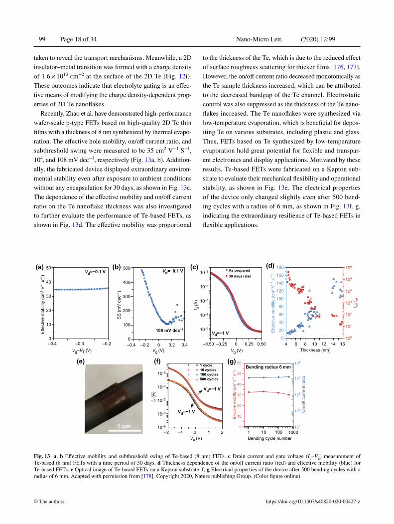
Recently, Zhao et al. have demonstrated high‑performance wafer‑scale p‑type FETs based on high‑quality 2D Te thin films with a thickness of 8 nm synthesized by thermal evapo‑ration. The effective hole mobility, on/off current ratio, and subthreshold swing were measured to be 35 cm2 V−1 S−1, 104, and 108 mV dec−1, respectively (Fig. 13a, b). Addition‑ally, the fabricated device displayed extraordinary environ‑mental stability even after exposure to ambient conditions without any encapsulation for 30 days, as shown in Fig. 13c. The dependence of the effective mobility and on/off current ratio on the Te nanoflake thickness was also investigated to further evaluate the performance of Te‑based FETs, as shown in Fig. 13d. The effective mobility was proportional
to the thickness of the Te, which is due to the reduced effect of surface roughness scattering for thicker films [176, 177]. However, the on/off current ratio decreased monotonically as the Te sample thickness increased, which can be attributed to the decreased bandgap of the Te channel. Electrostatic control was also suppressed as the thickness of the Te nano‑flakes increased. The Te nanoflakes were synthesized via low‑temperature evaporation, which is beneficial for depos‑iting Te on various substrates, including plastic and glass. Thus, FETs based on Te synthesized by low‑temperature evaporation hold great potential for flexible and transpar‑ent electronics and display applications. Motivated by these results, Te‑based FETs were fabricated on a Kapton sub‑strate to evaluate their mechanical flexibility and operational stability, as shown in Fig. 13e. The electrical properties of the device only changed slightly even after 500 bend‑ing cycles with a radius of 6 mm, as shown in Fig. 13f, g, indicating the extraordinary resilience of Te‑based FETs in flexible applications.
Bending cycle number
Bending radius 6 mm
On/
off c
urre
nt ra
tio
100
101
102
103
104
0
10
20
30
40
50
60
Effe
ctiv
e m
obillt
y (c
m2 V
–1 s
–1)
1 cycle10 cycles100 cycles500 cycles
50
40
30
20
10
0
500
400
300
200
100
0–0.4 –0.3 –0.2 –0.4 –0.50 –0.25
–2 –1 0 1 1 10 100 10002
10–5
10–6
10–7
10–8
10–9
10–5
10–6
10–7
10–8
10–9
100
101
102
103
104
105
106
0 0.25 0.50–0.2 0 0.2 0.4
108 mV dec–1
As prepared30 days later
Vd=−1 V
Vd=−1 V
Vg (V)Vg (V)
Va (V)
Vd=−0.1 VVd=−0.1 V
Vd=−1 V
Vg–VT (V)
I d (A
)
I d (A
)
4 6 8 10 12 14 16Thickness (nm)
180
160
140
120
100
80
60
40
20
0
Ette
ctiv
e m
obilit
y (c
m2 V
–1 s
–1)
Ette
ctiv
e m
obilit
y (c
m2 V
–1 s
–1)
SS (m
V de
c–1)
1 cm
(c)(b)(a) (d)
(g)(f)(e)I on
/I off
Fig. 13 a, b Effective mobility and subthreshold swing of Te‑based (8 nm) FETs. c Drain current and gate voltage (Id–Vg) measurement of Te‑based (8 nm) FETs with a time period of 30 days. d Thickness dependence of the on/off current ratio (red) and effective mobility (blue) for Te‑based FETs. e Optical image of Te‑based FETs on a Kapton substrate. f, g Electrical properties of the device after 500 bending cycles with a radius of 6 mm. Adapted with permission from [178]. Copyright 2020, Nature publishing Group. (Color figure online)

Nano‑Micro Lett. (2020) 12:99 Page 19 of 34 99
1 3
4.3 Piezoelectric Devices
Owing to the superior piezoelectric and mechanical perfor‑mance, and nanoscale structure, the piezoelectric effect in 2D materials has attracted considerable attention due to the potential applications, including energy converters, energy sources, sensors, and actuators. For example, due to the inversion asymmetry of monolayer MoS2, both experimen‑tal and theoretical investigations have proved that monolayer MoS2 exhibits piezoelectricity in its 2H phase [179–181]. However, the conversion rate of mechanical to electrical energy is severely restricted by its small piezoelectric coef‑ficient, which also limits its practical applications. In sharp contrast, 2D Te nanoflakes possess a large work function and the largest piezoelectric strain coefficient compared to the other existing piezoelectric materials [182]. Consequently, it has been a promising candidate for application in nanogen‑erators. Recently, He et al. [183] have demonstrated the first fully wearable and flexible nanogenerators with high output power based on low‑temperature, hydrothermally synthe‑sized 2D Te nanoflakes. The fabricated 2D Te nanogenera‑tor device was composed of a sandwich‑like structure with polydimethylsiloxane (PDMS)‑coated Te nanoflakes and Au/textile material, with the Au layer employed as the top and bottom electrodes. The devices were investigated in three bending states: flat, folded, and rolled, as shown in Fig. 14a, b. Under identical strains, periodic bending tests were car‑ried out, and a closed‑circuit current and an open‑circuit voltage of 290 nA and 3 V were achieved, respectively (Fig. 14c, d). In order to confirm the potential of the fabri‑cated 2D Te nanogenerator device for converting vibrational energy from human activities into electrical energy, the device was adhered to a human arm, and the corresponding
output current and voltage due to periodic bending and unbending were measured to be 650 nA and 2.5 V, respec‑tively. Additionally, when a compressive force of 8 N and an increased driving frequency of 10 Hz were applied to the device, the output power density was as high as 2.07 mW cm−2, which can power at least 10 LEDs. In order to get a better insight into the piezoelectric device based on 2D Te nanoflakes, Chen et al. carried out a systematic investigation of 2D Janus tellurene (Te2Se), including its piezoelectric properties and stability for monolayer and multilayer based on first‑principles calculations. According to the calculation for the monolayer 2D Janus tellurene, the flexible mechani‑cal properties and structural symmetry‑breaking give rise to large in‑plane and out‑of‑plane piezoelectric coefficients of 16.28 and 0.24 pm V−1, respectively. For multilayer 2D Janus tellurene, the applied in‑ and out‑of‑plane strains give rise to strong piezoelectric effects. Furthermore, certain stacking sequences lead to out‑of‑plane piezoelectric effects, while other sequences produced an in‑plane piezoelectric effect. Remarkably, the calculated piezoelectric coefficients of monolayer and multilayer 2D Janus tellurene were larger than that of the many Janus TMDCs and other well‑known piezoelectric materials.
4.4 Modulator
The superior properties of 2D Te nanoflakes, such as broad‑band optical absorption and response, strong light‑material interaction, and excellent environmental stability, enable 2D Te nanoflakes to be utilized for optical modulators. To gain insight into the modulation mechanism, Wu et al. designed an all‑optical modulation system based on 2D Te nanoflakes, with “on” and “off” modes for the modulating
i)(d)(c)(b)(a)
ii)iii)
Au/TextileAu/Textile
PDMSTFNG nanogenerator
talfelitxeT/uA
folded
rolled Volta
ge (V
)
Time (s) Time (s)0 1 2 3 4 50 1
1
0
2 3 4 5
Cur
rent
(nA)
Cur
rent
(nA)
–110
–50
–100
–1
–1
–100
–50
5
10
100
150
2.152.102.04Times (s)
150100
500
Au
Te NFTime (s)
0.15 0.10
Volla
ge (V
)
2
1
0
Fig. 14 a Schematic of the tellurene flexible nanogenerator (TFNG) device fabrication process. b Optical images of the TFNG devices in dif‑ferent states: flat, folded, and rolled. c, d Measurements of the output voltage and current due to periodic bending and unbending behavior. The insets show a single bending–unbending event. Adapted with permission from [183]. Copyright 2016, Elsevier

Nano‑Micro Lett. (2020) 12:99 99 Page 20 of 34
https://doi.org/10.1007/s40820‑020‑00427‑z© The authors
behavior [184]. The schematic of the system with 2D Te nanoflakes dispersions based on spatial cross‑phase modu‑lation is shown in Fig. 15a. Due to the combination of the Kerr and non‑axis‑symmetric thermal convection effects for both the pump and probe light, the diffraction rings were distorted, as seen in Fig. 15b. Moreover, the lower‑power probe light can be modulated by higher‑power pump light by using this modulation system, and the “on” and “off” modes can be realized (Fig. 15c). These outcomes show the 2D Te nanoflakes to be a promising candidate for photonics device applications. Motivated by the superior properties and great potential of 2D Te nanoflakes for modulator applications, Guo et al. successfully fabricated a saturable absorber
based on 2D Te/PVP nanoflakes, enabling the achievement of a highly stable femtosecond laser with a pulse duration of 829 fs (Fig. 15f) [185]. The 2D Te/PVP thin film was adhered to the end of a fiber and employed as a saturable absorber (Fig. 15d). The generated pulse train is shown in Fig. 15e, with a repetition frequency of 15.45 MHz. Moreo‑ver, no peak intensity fluctuation was found in the pulse train, illustrating the excellent stability of the mode‑locked laser operation. To further investigate the stability of the mode‑locked laser, radio‑frequency (RF) spectrum meas‑urement was carried out, as shown in Fig. 15g. The peak was measured, displaying a frequency and peak‑to‑back‑ground ratio of 15.45 MHz and 53 dB, respectively. These
Sample
LensBS
671 nm laser
532 nm laser
(b)(a) (c)
(g)(f)
Prob
e lig
ht (μ
W) 25
201510
50
60 80 100 120 140Pump light (mW)
Experiment FittingOn
Off
(e)(d)
PC30% OC
2D Te/PVP SA ISOEDF
WDM
Pump
Inte
nsity
(a.u
.)
(h) (i)Time (ns) Delay (ps) Frenquency (MHz)
(j)
Modulation Frequency (Hz)Modulation Frequency (Hz)
Experimental data
Sech2 fitting
–3–400 –200 0 200 400 –2 –1 0 1 2 3
Inte
nsity
(n.u
.)
Inte
nsity
(dBm
)
1.00.80.60.40.20.0
–60
–80
–100
–120
–14015.5 17.0 18.5
1.0
0.9
0.8
0.7
0.6
0.5
0.4
0.3
0.2
0.1
0
Ener
gy/B
it (J
)
10–10
10–11
10–10
10–9
109 1010 1011 1012 1013 109 1010 1011
10–9
10–3
Ener
gy/B
it (J
)
100 ns div−1
65.2 ns
2
1
0
10 nm20 nm30 nm40 nm50 nm60 nm70 nm80 nm
10 nm20 nm30 nm40 nm50 nm60 nm70 nm80 nm
f=15.45 MHzS/N:=53 dB
–50
–70
–90
–110
–130
–150
20 40 60 80 100 120
1 2
3 4
829 fs0.6481.28 ps=400 ns div−1
Fig. 15 a Schematic of the all‑optical modulator system based on 2D Te nanoflakes. b Diffraction rings produced by the all‑optical modulator system. c Output of the all‑optical switcher based on 2D Te nanoflakes as a function of pump laser power including the theoretical fit. Adapted with permission from [184]. Copyright 2019, WILEY–VCH. d Schematic of the mode‑locking erbium‑doped fiber laser based on a 2D Te/PVP thin film. e Pulse trains from the fiber laser. Inset: 4 μs pulse trains. f Pulse duration of the modulated femtosecond laser. g Radio‑frequency spectrum of the fiber laser. Inset: broadband radio‑frequency spectrum. Adapted with permission from [185]. Copyright 2019, The Royal Soci‑ety of Chemistry. h Calculated electric and optical field profiles in the modulator. i Simulated energy consumption of the modulator as a function of frequency for different thicknesses of 2D Te nanoflakes. Inset: schematic of the Mach–Zehnder interferometer (MZI) modulator. j Calculated energy consumption of the Te racetrack modulator as a function of frequency for different thicknesses of tellurene. Inset: schematic of the race‑track modulator. Adapted with permission from [137]. Copyright 2019, American Chemical Society

Nano‑Micro Lett. (2020) 12:99 Page 21 of 34 99
1 3
outcomes further confirmed the extraordinary stability of the mode‑locked laser operation. Furthermore, the satura‑tion intensities (modulation depths) of the Te/PVP thin films were measured to be 44.65 (11.86%), 26 (10.5%), and 78.14 (27%) GW cm−2 at 800, 1060, and 1550 nm, respectively, which confirmed that Te/PVP thin films show great potential for broadband saturable absorber and mode‑locking laser applications. As mentioned previously, similar to BP, 2D Te has a tunable bandgap range of 0.35–1.2 eV, which covers the MIR spectral band up to a wavelength of 3.5 μm. Several kinds of MIR modulators have been demonstrated using free carrier plasma dispersion [186, 187], thermo‑optic phase shift [188–190], electro‑absorption (Pauli blocking or field‑induced effects) [191–193], and the electro‑refractive (Pock‑els) effect [194]. Among these technologies, Pockels electro‑optic modulators were the most popular modulator due to their intrinsic ultrafast response and potential for achieving phase‑only modulation. However, MIR integrated Pockels modulators have only been experimentally realized using Si‑on‑LiNbO3 [194]. The broken structural inversion sym‑metry and huge electro‑optic activity of 2D Te permit it to be utilized for low energy and ultrafast Pockels effect modula‑tors. In this regard, Jones et al. reported a high‑performance waveguide‑integrated Pockels effect modulator based on 2D Te. The modulator showed a switching energy of 12.0 pJ/bit and a half‑wave voltage‑length product of 2.7 V cm, which is orders of magnitude higher than that of existing state‑of‑the‑art devices (Fig. 15h–j) [137].
4.5 Energy Harvesting Devices
Due to the rapid pace of industrial development, the energy crisis has become a critical issue in the twenty‑first century. During the past decade, there have been tremendous efforts to solve this severe worldwide problem [195–200]. The gen‑eration of electricity through harvesting energy from ambi‑ent and waste heat sources is an environmentally friendly and sustainable approach to overcome this problem. In general, two solutions have been proposed to improve thermoelec‑tric generation efficiency: striving to develop high‑efficiency thermoelectric bulk materials or low‑dimension thermoelec‑tric materials. As previously mentioned, a large body of the‑oretical and experimental investigations has proved that 2D Te possesses extraordinary thermoelectric properties, even among the other 2D materials [185, 201–205]. Thus, 2D
Te holds great potential for next‑generation thermoelectric device applications. Recently, by combining the advantages of nanostructures and the intrinsically high thermoelectric property of 2D Te, Qiu et al. [202] have presented the first highly efficient thermoelectric devices based on 2D Te, as shown in Fig. 16a. A He–Ne laser was employed to locally heat the 2D Te and generate a temperature gradient. Ther‑moelectric current mapping measurements were taken to further improve the harvesting efficiency. Figure 16b pre‑sents the laser‑induced thermoelectric current mapping of the fabricated device. Noticeably, a thermoelectric current of almost 3 μA was achieved for an incident laser power of 3 mW, which is two orders of magnitude larger than that of previous investigations [206, 207]. However, a photovoltaic effect may exist during the measurement and contribute to the generated current. To evaluate of the influence of photo‑voltaic effect during the measurement process, three differ‑ent types of metals were used as electrodes. According to the outcomes, the photovoltaic effect generated a current located at the metal–semiconductor interface, and a depletion‑type contact was formed, as shown in Fig. 16c. Solar energy is another important reliable source of energy in nature. Many efforts have attempted to efficiently take advantage of this energy source. Solar cells, which can convert sunlight into electricity, have already proven to be a lucrative candidate for commercialization applications and continue to be an extremely popular and diverse area of research. To further enhance the conversion efficiency and performance of solar cells, heterojunction solar cells are currently in the research and development phase. This type of solar cell requires a suitable direct bandgap of 1.2–1.6 eV, high carrier mobil‑ity, and environmental stability. It has been shown that 2D tellurene meets almost all the aforementioned criteria [208]. Recently, Wu et al. [209] have theoretically demonstrated a high‑efficiency heterojunction solar cell based on 2D Te and TMDCs. By utilizing first‑principles DFT simulations, the maximum power conversion efficiency of the 2D Te/WTe2 and 2D Te/MoTe2 heterojunction solar cells was calculated to be 22.5% and 20.1%, respectively, as shown in Fig. 16d. In addition, the heterojunctions exhibited a remarkable absorp‑tion of sunlight and an enhancement of charge separation behavior due to the type‑II band alignment. Utilizing pure 2D ternary compounds, Yang et al. [210] reported a highly efficient solar cell based on monolayer HfTeSe4. The simu‑lation outcomes from first‑principles calculations indicated that the solar cell exhibited an extraordinary absorbance

Nano‑Micro Lett. (2020) 12:99 99 Page 22 of 34
https://doi.org/10.1007/s40820‑020‑00427‑z© The authors
coefficient of up to 105 cm−1 in the visible band, as shown in Fig. 16e. The monolayer HfTeSe4 exhibited a relative long carrier recombination lifetime and ultrahigh photocurrent (Fig. 16f, g), which is beneficial for solar cell applications. The calculated maximum power conversion efficiency of solar cell based on a monolayer HfTeSe4 and Bi2WO6 het‑erojunction is up to 20.8% (Fig. 16h), which is much higher than that of 2D organic and heterostructure‑based solar cells reported previously [211–214]. To aid in the comparison with existing devices, the figures‑of‑merit of some typical
energy harvesting devices based on 2D materials are listed in Table 3. The comparison results indicate that 2D Te is suitable for high‑performance energy harvesting devices.
4.6 Logic Gates and Circuits
Benefiting from the high uniformity of Te FETs, which ena‑bles the fabrication of logic gates and computational circuits based on Te FETs, Javey et al. have recently demonstrated various functional logic gates and circuits based on p‑type
Band gap (eV)Energy (eV)
Con
duct
ion
band
offs
et (e
V)Energy (eV) Time (fs)
30002000100000.88
0.92Popu
latio
n
1.00
0.96
τ=26 ps
τ=54 ps
τ=76 ps
–2%0%2%
3.53.02.52.01.51.00.50
1x10⁵
2x10⁵
3x10⁵
4x10⁵
5x10⁵
6x10⁵
InSeMoS2
HfTeSe2–yHfTeSe4–x
α(ω
) (cm
–1)
17.5(Te/MoSe2)
10.6(Te/MoS2)
22.5(Te/WTe2)18.7(Te/WSe2)
18.8(Te/WS2)20.1(Te/MoTe2)
Power Conversion Efficiency (%)0.8
0.7
0.6
0.5
0.4
0.3
0.2
0.1
0.0
Con
duct
ion
Band
Offs
et (e
V)
1.0 1.2 1.4 1.6 1.8 2.00
5
10
16
20
Band Gap of Donor (eV)
30
25
20
15
10
5
00.5 1.0 1.5 2.0 2.5 3.0 3.5 1.0 1.5 2.0 2.5 3.0
1.2
1.0
0.8
0.6
0.4
0.2
0.020.8%
22.8%
xy
J ph
(A m
−2)
IPVITE ITE IPV CrCr
Depletion-typeCurrent (μA)
x (μm)
Y (μ
m)
3
0
–3
00
5
10
15
5 10 15
(c)(b)(a)
(f)(e)
(g) (h)
(d)
Fig. 16 a Schematic of the thermoelectric device using 2D Te. b Laser‑induced thermoelectric current mapping of the device. c Band diagrams of the depletion‑type device due to the combined photoelectric and thermoelectric effects. Adapted with permission from [202]. Copyright 2019, American Chemical Society. d Power conversion efficiency of 2D Te/TMDCs heterojunction solar cells as a function of the conduction band off‑set and the donor bandgap. Adapted with permission from [209]. Copyright 2019, The Royal Society of Chemistry. e Absorption coefficients of monolayer HfTeSe4 compared to MoS2 and InSe. f Carrier recombination lifetime under different biaxial strains. g Photocurrents of monolayer HfTeSe4 as a function of photon energy along the x‑ and y‑direction. h Power conversion efficiency of the HfTeSe4/Bi2WO6 heterostructure‑based solar cell with and without a 2% tensile strain. Adapted with permission from [210]. Copyright 2019, American Chemical Society
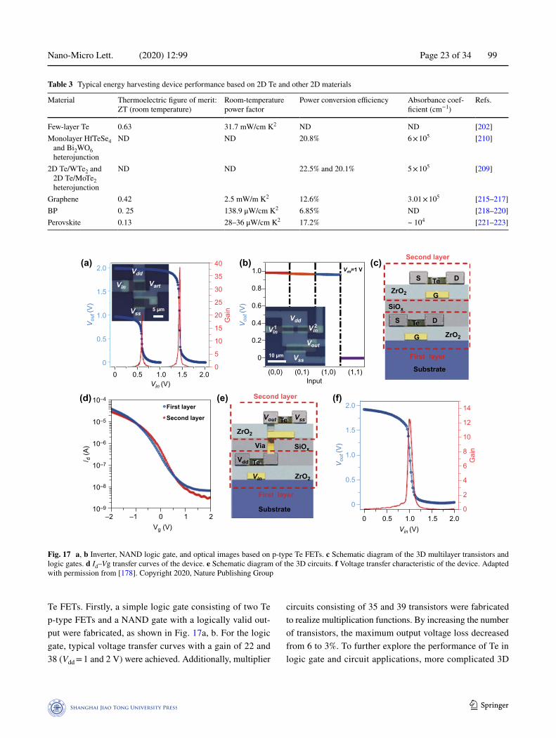
Nano‑Micro Lett. (2020) 12:99 Page 23 of 34 99
1 3
Te FETs. Firstly, a simple logic gate consisting of two Te p‑type FETs and a NAND gate with a logically valid out‑put were fabricated, as shown in Fig. 17a, b. For the logic gate, typical voltage transfer curves with a gain of 22 and 38 (Vdd = 1 and 2 V) were achieved. Additionally, multiplier
circuits consisting of 35 and 39 transistors were fabricated to realize multiplication functions. By increasing the number of transistors, the maximum output voltage loss decreased from 6 to 3%. To further explore the performance of Te in logic gate and circuit applications, more complicated 3D
Table 3 Typical energy harvesting device performance based on 2D Te and other 2D materials
Material Thermoelectric figure of merit: ZT (room temperature)
Room‑temperature power factor
Power conversion efficiency Absorbance coef‑ficient (cm−1)
Refs.
Few‑layer Te 0.63 31.7 mW/cm K2 ND ND [202]Monolayer HfTeSe4
and Bi2WO6 heterojunction
ND ND 20.8% 6 × 10⁵ [210]
2D Te/WTe2 and 2D Te/MoTe2 heterojunction
ND ND 22.5% and 20.1% 5 × 10⁵ [209]
Graphene 0.42 2.5 mW/m K2 12.6% 3.01 × 10⁵ [215–217]BP 0. 25 138.9 μW/cm K2 6.85% ND [218–220]Perovskite 0.13 28–36 μW/cm K2 17.2% ~ 104 [221–223]
00
0.5
1.0
1.5
2.0
0
0.5
1.0
1.5
2.0
0.5 1.0 1.5 2.00
5
10
15
20
25
30
35
40
Gai
n
0
2
4
6
8
10
12
14
Gai
n
1.0
0.8
0.6
0.4
0.2
0
(0,0) (0,1) (1,0) (1,1)Input
Vdd=1 V
Second layer
Second layer
S Te
Te
D
G
DS Te
G ZrO2
ZrO2
ZrO2
Substrate
First layer
Substrate
First layer
0 0.5 1.0 1.5 2.0
First layer
Second layer
ZrO2
SiOx
SiOx
Vdd
Vdd
Vin
Vin
Vout Vss
Vdd
Vou
t (V)
Vou
t (V)
Vou
t (V)
Vin (V)
Vin (V)
Vin
Vss
Vart
Vout
Vss
10–4
10–5
10–6
10–7
10–8
10–9
–2 –1 0 1 2Vg (V)
/ d (A
) Via
Te
2Vin1
10 µm
5 µm
(c)(b)(a)
(f)(e)(d)
Fig. 17 a, b Inverter, NAND logic gate, and optical images based on p‑type Te FETs. c Schematic diagram of the 3D multilayer transistors and logic gates. d Id–Vg transfer curves of the device. e Schematic diagram of the 3D circuits. f Voltage transfer characteristic of the device. Adapted with permission from [178]. Copyright 2020, Nature Publishing Group

Nano‑Micro Lett. (2020) 12:99 99 Page 24 of 34
https://doi.org/10.1007/s40820‑020‑00427‑z© The authors
multilayer transistors and logic gates based on p‑type Te FETs were demonstrated, as shown in Fig. 17c. Noticeably, the Id–Vg transfer curves of the first layer changed slightly after the construction of the top layer through a low‑tem‑perature process, as shown in Fig. 17d. The slight shift of the threshold voltage was likely caused by the semicon‑ductor–oxide interface or a fixed charge in the intermedi‑ate oxide. A two‑layer invert was employed to construct 3D circuits, where the upper‑ and bottom‑layer transistors were operated as an active load and the driver, respectively (Fig. 17e). A gain of approximately 12 at a Vdd = 2 V was achieved, as shown in Fig. 17f. These outcomes indicate that p‑type Te FETs possess great potential for integrated 3D logic gates and circuits applications [178].
5 Summary
Since 2D Te nanoflakes were successfully fabricated in 2017, it has become one of the most popular of the 2D mate‑rials family [183]. In this review, we summarized the crystal structure, synthesis methods, physical properties, and vari‑ous applications based on 2D Te nanoflakes, such as pho‑todetectors, FETs, piezoelectric devices, modulators, logic gates, and circuits. Similar to BP, 2D Te nanoflakes are a layered semiconductor material with a thickness‑dependent bandgap ranging from 0.35 to 1.2 eV (visible to MIR band). The unique helical chain structure of 2D Te gives rise to a high room‑temperature carrier mobility (~ 103 cm2 V−1 s−1) and strong in‑plane anisotropic properties. In sharp contrast, due to an energy barrier that inhibits oxidation pathways, 2D Te nanoflakes possess more robust environmental stability than other existing 2D materials, making them a promis‑ing material for fundamental research as well as practical applications. During the past two decades, it has become highly sought after to obtain large‑scale and high‑quality 2D materials to satisfy the demands of various applications arising from the rapid development of the semiconductor industry. Up scaling the fabrication of these 2D materials is currently a major area of focus in the nanotechnology and nanoscience field, and the lack of commercially viable solutions is also severely restricting the further development of 2D materials in the semiconductor industry. However, scalable and high‑quality 2D Te nanoflakes can be efficiently synthesized though various means, including PVD, MBE, solution synthesis, LPE methods, and thermal evaporation.
These low‑cost and efficient synthesis methods are favorable for industry applications and commercialization.
As a versatile material, 2D Te nanoflakes have been utilized in a wide range of applications. The unique helical chain structure, flexible mechanical properties, and struc‑tural symmetry‑breaking in 2D Te nanoflakes lead to a large in‑plane piezoelectric coefficient, which enable it to be a potential material for piezoelectric devices. Moreover, benefiting from air‑stability, strong light‑material interac‑tion, broadband optical absorption and response, and other superior properties, 2D Te nanoflakes have been utilized in the fabrication of numerous devices, including photo‑detectors, FETs, modulators, logic gates and circuits, and exhibited excellent performance that often exceeds the existing state‑of‑the‑art 2D materials.
6 Prospective
Although 2D Te nanoflakes have already shown excel‑lent potential for academic and engineering applications (Fig. 18), challenges and opportunities still remain for researchers. For synthesis processes, ultrathin 2D Te nanoflakes can be synthesized through the PVD method. However, the requirements for a high‑vacuum environ‑ment and high‑purity atomic sources limit the potential for up scaling. The LPE technique is an effective means of synthesizing layered 2D Te nanoarchitectures. However,
Modulator
Phot
odet
ec
tor
Logicgate
&circuits
FETs
SynthesisEnerg
y harv
estin
g
Piezoelectric
PropertiesStru
ctur
e
Fig. 18 The academic and engineering applications of 2D Te nano‑flakes

Nano‑Micro Lett. (2020) 12:99 Page 25 of 34 99
1 3
the small‑scale and inefficient control of the thickness of the derived materials restricts its further applications. Additionally, in situ CVD methods have been applied to synthesize large‑scale and high‑quality 2D materials, such as graphene, BP, and TMDCs among others [224–233]. However, the use of CVD method is rarely reported to produce ultrathin 2D Te nanoflakes. Thus, it is of great significance to develop CVD techniques to grow atomi‑cally thin Te. In particular, the controllable synthesis of a desired number of layers from monolayer to multilayer is highly sought after.
Regarding photodetectors and FETs based on 2D Te nano‑flakes, the reported investigations mainly focus on the visible to near‑IR band. The development of ultra‑broadband (UV to MIR band) devices is highly preferred. Additionally, the car‑rier dynamics and transport mechanisms in photodetectors and FETs are not understood clearly enough compared to photodetectors and FETs based on BP and TMDCs. Further‑more, doping and heterojunction methods can significantly enhance the performance of photodetectors and FETs based on 2D Te nanoflakes. To further improve the performance of Te‑based devices, it is necessary to improve the doping and heterojunction fabrication techniques, particularly control‑lable doping and heterojunction formation processes. Fur‑ther investigations are necessary to gain a better insight into photodetectors and FETs based on 2D Te nanoflakes. In the modulator application, the long‑term operation stability is still a challenge. Additionally, only a few investigations have been reported examining free‑space and waveguide modula‑tors based on 2D Te nanoflakes. Further research is needed to explore the performance and mechanisms of these modu‑lators. For energy harvesting devices, most investigations are still in the theoretical stage and further experimental work is needed to provide a pathway toward helping solve the energy crisis. In logic gate applications, the use of 2D Te has only been achieved in the simplest logic gate. Further investi‑gations should be carried out to explore the performance of p‑type Te FET‑based logic gates with more complicated structures. For circuit applications, the practicality of p‑type Te FETs has only been demonstrated for monolithic 3D cir‑cuits. To enhance the performance of such devices, a more suitable insulation layer and a more optimized deposition technique must be found.
Besides the aforementioned applications, extending the applications of 2D Te thin films to other fields, such as flexible and transparent electronics and displays, highly
integrated chips, biomedicine, and lasing has become a criti‑cal issue for its further development. With the rapid devel‑opment of 2D materials and industry demands, we believe 2D Te will continue to find novel applications in the future.
In conclusion, 2D Te is a fascinating material due to its excellent properties and great potential in various fundamen‑tal and practical applications. However, 2D Te also faces some significant challenges. The continued investigation of this interesting material in photonic systems, including pho‑todetectors, FETs, piezoelectric devices, modulators, energy harvesting devices, logic gates, and circuits, is anticipated. A more comprehensive understanding of 2D Te nanoflakes will emerge in the future as a result of these ongoing concerted research efforts.
Acknowledgements The research was partially supported by the National Natural Science Fund of China (Grant Nos. 61875138, 61435010, and 61961136001); Science and Technology Innova‑tion Commission of Shenzhen (KQJSCX20180328095501798, JCYJ20180507182047316, KQTD2015032416270385, JCYJ20170811093453105, JCYJ20180307164612205 and GJHZ20180928160209731); Natural Science Foundation of Guangdong Province for Distinguished Young Scholars (2018B030306038); and Natural Science Foundation of SZU (No. 860‑000002110429). Authors also acknowledge the support from Instrumental Analysis Center of Shenzhen University (Xili Campus).
Open Access This article is licensed under a Creative Commons Attribution 4.0 International License, which permits use, sharing, adaptation, distribution and reproduction in any medium or format, as long as you give appropriate credit to the original author(s) and the source, provide a link to the Creative Commons licence, and indicate if changes were made. The images or other third party material in this article are included in the article’s Creative Com‑mons licence, unless indicated otherwise in a credit line to the material. If material is not included in the article’s Creative Com‑mons licence and your intended use is not permitted by statutory regulation or exceeds the permitted use, you will need to obtain permission directly from the copyright holder. To view a copy of this licence, visit http://creat iveco mmons .org/licen ses/by/4.0/.
References
1. L.A. Ba, M. Doering, V. Jamier, C. Jacob, Tellurium: an element with great biological potency and potential. Org. Biomol. Chem. 8(19), 4203–4216 (2010). https ://doi.org/10.1039/c0Ob0 0086h
2. J.W. Liu, J.H. Zhu, C.L. Zhang, H.W. Yu, S.H. Liang, Meso‑structured assemblies of ultrathin superlong tellurium nanow‑ires and their photoconductivity. J. Am. Chem. Soc. 132(26), 8945–8952 (2010). https ://doi.org/10.1021/ja910 871s
Nano‑Micro Lett. (2020) 12:99 99 Page 26 of 34
https://doi.org/10.1007/s40820‑020‑00427‑z© The authors
3. H. Peng, N. Kioussis, G.J. Snyder, Elemental tellurium as a chiral p‑type thermoelectric material. Phys. Rev. B 89(19), 195206 (2014). https ://doi.org/10.1103/PhysR evB.89.19520 6
4. J.P. Hermann, G. Quentin, J.M. Thuillier, Determina‑tion of the d14 piezoelectric coefficient of tellurium. Solid State Commun. 7(1), 161–163 (1969). https ://doi.org/10.1016/0038‑1098(69)90715 ‑7
5. K.S. Novoselov, A.K. Geim, S.V. Morozov, D. Jiang, Y. Zhang, S.V. Dubonos, I.V. Grigorieva, A.A. Firsov, Elec‑tric field effect in atomically thin carbon films. Science 306(5696), 666–669 (2004). https ://doi.org/10.1126/scien ce.11028 96
6. K.S. Novoselov, A.K. Geim, S.V. Morozov, D. Jiang, M.I. Katsnelson, I.V. Grigorieva, S.V. Dubonos, A.A. Firsov, Two‑dimensional gas of massless dirac fermions in graphene. Nature 438(7065), 197–200 (2005). https ://doi.org/10.1038/natur e0423 3
7. Y. Yin, R. Cao, J. Guo, C. Liu, J. Li et al., High‑speed and high‑responsivity hybrid silicon/black‑phosphorus waveguide photodetectors at 2 μm. Laser Photonics Rev. 13(6), 1900032 (2019). https ://doi.org/10.1002/lpor.20190 0032
8. C. Xing, G. Jing, X. Liang, M. Qiu, Z. Li et al., Graphene oxide/black phosphorus nanoflake aerogels with robust thermo‑stability and significantly enhanced photothermal properties in air. Nanoscale 9(24), 8096–8101 (2017). https ://doi.org/10.1039/c7nr0 0663b
9. A.C. Ferrari, J.C. Meyer, V. Scardaci, C. Casiraghi, M. Lazzeri et al., Raman spectrum of graphene and graphene layers. Phys. Rev. Lett. 97(18), 187401 (2006). https ://doi.org/10.1103/PhysR evLet t.97.18740 1
10. J. Wang, H. Yan, Z. Liu, Z. Wang, H. Gao et al., Langmuir‑Blodgett self‑assembly of ultrathin graphene quantum dot films with modulated optical properties. Nanoscale 10(41), 19612–19620 (2018). https ://doi.org/10.1039/c8nr0 5159c
11. Q. Bao, H. Zhang, B. Wang, Z. Ni, C.H.Y.X. Lim, Y. Wang, D.Y. Tang, K.P. Loh, Broadband graphene polarizer. Nat. Photonics 5(7), 411–415 (2011). https ://doi.org/10.1038/nphot on.2011.102
12. S. Lu, C. Zhao, Y. Zou, S. Chen, Y. Chen, Y. Li, H. Zhang, S. Wen, D. Tang, Third order nonlinear optical property of Bi2Se3. Opt. Express 21(2), 2072–2082 (2013). https ://doi.org/10.1364/oe.21.00207 2
13. Z. Zheng, C. Zhao, S. Lu, Y. Chen, Y. Li, H. Zhang, S. Wen, Microwave and optical saturable absorption in graphene. Opt. Express 20(21), 23201–23214 (2012). https ://doi.org/10.1364/oe.20.02320 1
14. H. Yu, H. Zhang, Y. Wang, C. Zhao, B. Wang, S. Wen, H. Zhang, J. Wang, Topological insulator as an optical modula‑tor for pulsed solid‑state lasers. Laser Photonics Rev. 7(6), L77–L83 (2013). https ://doi.org/10.1002/lpor.20130 0084
15. M. Qiu, D. Wang, W. Liang, L. Liu, Y. Zhang et al., Novel concept of the smart nir‑light‑controlled drug release of black phosphorus nanostructure for cancer therapy. Proc. Natl. Acad. Sci. U.S.A. 115(3), 501–506 (2018). https ://doi.org/10.1073/pnas.17144 21115
16. A.H. Neto, F. Guinea, N.M.R. Peres, K.S. Novoselov, A.K. Geim, The electronic properties of graphene. Rev. Mod. Phys. 81(1), 109–162 (2009). https ://doi.org/10.1103/RevMo dPhys .81.109
17. H. Zhang, S. Virally, Q. Bao, L.K. Ping, S. Massar, N. God‑bout, P. Kockaert, Z‑scan measurement of the nonlinear refractive index of graphene. Opt. Lett. 37(11), 1856–1858 (2012). https ://doi.org/10.1364/ol.37.00185 6
18. S.B. Lu, L.L. Miao, Z.N. Guo, X. Qi, C.J. Zhao et al., Broad‑band nonlinear optical response in multi‑layer black phos‑phorus: an emerging infrared and mid‑infrared optical mate‑rial. Opt. Express 23(9), 11183–11194 (2015). https ://doi.org/10.1364/oe.23.01118 3
19. R. Cao, H.D. Wang, Z.N. Guo, D.K. Sang, L.Y. Zhang et al., Black phosphorous/indium selenide photoconductive detector for visible and near‑infrared light with high sensitivity. Adv. Opt. Mater. 7(12), 1900020 (2019). https ://doi.org/10.1002/adom.20190 0020
20. Q. Zhou, Q. Chen, Y. Tong, J. Wang, Light‑induced ambi‑ent degradation of few‑layer black phosphorus: mechanism and protection. Angew. Chem. Int. Ed. 55(38), 11437–11441 (2016). https ://doi.org/10.1002/anie.20160 5168
21. J. Zheng, Z. Yang, C. Si, Z. Liang, X. Chen et al., Black phosphorus based all‑optical‑signal‑processing: toward high performances and enhanced stability. ACS Photonics 4(6), 1466–1476 (2017). https ://doi.org/10.1021/acsph otoni cs.7b002 31
22. M.H. Jeong, D.H. Kwak, H.S. Ra, A.Y. Lee, J.S. Lee, Real‑izing long‑term stability and thickness control of black phosphorus by ambient thermal treatment. ACS Appl. Mater. Interfaces 10(22), 19069–19075 (2018). https ://doi.org/10.1021/acsam i.8b046 27
23. H. Zhang, S.B. Lu, J. Zheng, J. Du, S.C. Wen, D.Y. Tang, K.P. Loh, Molybdenum disulfide (MoS) as a broadband sat‑urable absorber for ultra‑fast photonics. Opt. Express 22(6), 7249–7260 (2014). https ://doi.org/10.1364/oe.22.00724 9
24. B. Wu, X. Liu, J. Yin, H. Lee, Bulk β‑Te to few layered β‑tellurenes: indirect to direct band‑gap transitions showing semiconducting property. Mater. Res. Express 4(9), 095902 (2017). https ://doi.org/10.1088/2053‑1591/aa8ae 3
25. Y. Wang, G. Qiu, R. Wang, S. Huang, Q. Wang et al., Field‑effect transistors made from solution‑grown two‑dimensional tellurene. Nat. Electron. 1(4), 228–236 (2018). https ://doi.org/10.1038/s4192 8‑018‑0058‑4
26. M. Amani, C. Tan, G. Zhang, C. Zhao, J. Bullock et al., Solution‑synthesized high‑mobility tellurium nanoflakes for short‑wave infrared photodetectors. ACS Nano 12(7), 7253–7263 (2018). https ://doi.org/10.1021/acsna no.8b034 24
27. A. Vonhippel, Structure and conductivity in the vib group of the periodic system. J. Chem. Phys. 16(4), 372–380 (1948). https ://doi.org/10.1063/1.17468 93
28. W. Zhang, Q. Wu, O.V. Yazyev, H. Weng, Z. Guo, W.‑D. Cheng, G.‑L. Chai, Topological phase transitions driven by strain in monolayer tellurium. Phys. Rev. B 98(11), 115411 (2018). https ://doi.org/10.1103/PhysR evB.98.11541 1

Nano‑Micro Lett. (2020) 12:99 Page 27 of 34 99
1 3
29. C. Lin, W. Cheng, G. Chai, H. Zhang, Thermoelectric properties of two‑dimensional selenene and tellurene from group‑VI elements. Phys. Chem. Chem. Phys. 20(37), 24250–24256 (2018). https ://doi.org/10.1039/C8CP0 4069A
30. A.K. Geim, Graphene: status and prospects. Science 324(5934), 1530–1534 (2009). https ://doi.org/10.1126/scien ce.11588 77
31. L.M. Malard, M.A. Pimenta, G. Dresselhaus, M.S. Dres‑selhaus, Raman spectroscopy in graphene. Phys. Rep. Rev. Sect. Phys. Lett. 473(5–6), 51–87 (2009). https ://doi.org/10.1016/j.physr ep.2009.02.003
32. Y. Zhu, S. Murali, M.D. Stoller, K.J. Ganesh, W. Cai et al., Carbon‑based supercapacitors produced by activation of graphene. Science 332(6037), 1537–1541 (2011). https ://doi.org/10.1126/scien ce.12007 70
33. C.N.R. Rao, A.K. Sood, K.S. Subrahmanyam, A. Govin‑daraj, Graphene: the new two‑dimensional nanomaterial. Angew. Chem. Int. Ed. 48(42), 7752–7777 (2009). https ://doi.org/10.1002/anie.20090 1678
34. Q. Bao, H. Zhang, Z. Ni, Y. Wang, L. Polavarapu et al., Monolayer graphene as a saturable absorber in a mode‑locked laser. Nano Res. 4(3), 297–307 (2011). https ://doi.org/10.1007/s1227 4‑010‑0082‑9
35. K.T. Chen, M.H. Hsieh, Y.S. Su, J. Wen, S.T. Chang, Car‑rier mobility calculation for monolayer black phosphorous. J. Nanosci. Nanotechnol. 19(10), 6821–6825 (2019). https ://doi.org/10.1166/jnn.2019.17126
36. T. Vy, R. Soklaski, Y. Liang, L. Yang, Layer‑controlled band gap and anisotropic excitons in few‑layer black phosphorus. Phys. Rev. B 89(23), 235319 (2014). https ://doi.org/10.1103/PhysR evB.89.23531 9
37. N. Youngblood, C. Chen, S.J. Koester, M. Li, Waveguide‑integrated black phosphorus photodetector with high respon‑sivity and low dark current. Nat. Photonics 9(4), 247–252 (2015). https ://doi.org/10.1038/nphot on.2015.23
38. Q. Jiang, L. Xu, N. Chen, H. Zhang, L. Dai, S. Wang, Facile synthesis of black phosphorus: an efficient electrocatalyst for the oxygen evolving reaction. Angew. Chem. Int. Ed. 55(44), 13849–13853 (2016). https ://doi.org/10.1002/anie.20160 7393
39. H. Mu, S. Lin, Z. Wang, S. Xiao, P. Li et al., Black phos‑phorus‑polymer composites for pulsed lasers. Adv. Opt. Mater. 3(10), 1447–1453 (2015). https ://doi.org/10.1002/adom.20150 0336
40. J. Shao, H. Xie, H. Huang, Z. Li, Z. Sun et al., Biodegradable black phosphorus‑based nanospheres for in vivo photother‑mal cancer therapy. Nat. Commun. 7, 12967 (2016). https ://doi.org/10.1038/ncomm s1296 7
41. Q. Bao, H. Zhang, Y. Wang, Z. Ni, Y. Yan, Z.X. Shen, K.P. Loh, D.Y. Materials, Atomic‑layer graphene as a saturable absorber for ultrafast pulsed lasers. Adv. Funct. Mater. 19(19), 3077–3083 (2009). https ://doi.org/10.1002/adfm.20090 1007
42. K.F. Mak, C. Lee, J. Hone, J. Shan, T.F. Heinz, Atomically thin MoS2: a new direct‑gap semiconductor. Phys. Rev. Lett. 105(13), 136805 (2010). https ://doi.org/10.1103/PhysR evLet t.105.13680 5
43. A. Splendiani, L. Sun, Y. Zhang, T. Li, J. Kim, C.‑Y. Chim, G. Galli, F. Wang, Emerging photoluminescence in mon‑olayer MoS2. Nano Lett. 10(4), 1271–1275 (2010). https ://doi.org/10.1021/nl903 868w
44. Z. Wang, D. Gresch, A.A. Soluyanov, W. Xie, S. Kushwaha et al., MoTe2: a type‑ii weyl topological metal. Phys. Rev. Lett. 117(5), 056805 (2016). https ://doi.org/10.1103/PhysR evLet t.117.05680 5
45. M. Liu, X.W. Zheng, Y.L. Qi, H. Liu, H. Zhang, Microfiber‑based few‑layer MoS2 saturable absorber for 2.5 Ghz pas‑sively harmonic mode‑locked fiber laser. Opt. Express 22(19), 22841–22846 (2014). https ://doi.org/10.1364/OE.22.02284 1
46. J. Du, Q. Wang, G. Jiang, C. Xu, C. Zhao, Y. Xiang, Y. Chen, S. Wen, H. Zhang, Ytterbium‑doped fiber laser passively mode locked by few‑layer molybdenum disulfide (MoS2) saturable absorber functioned with evanescent field interac‑tion. Sci. Rep. 4, 6346 (2014). https ://doi.org/10.1038/srep0 6346
47. L. Lu, Z. Liang, L. Wu, Y. Chen, Y. Song et al., Few‑layer bismuthene: sonochemical exfoliation, nonlinear optics and applications for ultrafast photonics with enhanced stability. Laser Photonics Rev. 12(1), 1700221 (2018). https ://doi.org/10.1002/lpor.20170 0221
48. D.A. Bandurin, A.V. Tyurnina, G.L. Yu, A. Mishchenko, V. Zolyomi et al., High electron mobility, quantum hall effect and anomalous optical response in atomically thin InSe. Nat. Nanotechnol. 12(3), 223–227 (2017). https ://doi.org/10.1038/nnano .2016.242
49. X. Zhou, L. Gan, W. Tian, Q. Zhang, S. Jin, H. Li, Y. Bando, D. Golberg, T. Zhai, Ultrathin SnSe2 flakes grown by chemical vapor deposition for high‑performance photo‑detectors. Adv. Mater. 27(48), 8035–8041 (2015). https ://doi.org/10.1002/adma.20150 3873
50. W. Chen, H. Luo, Z. Han, C. Li, L. Yong, Passively Q‑switched mid‑infrared fluoride fiber laser around 3 μm using a tungsten disulfide (WS2) saturable absorber. Laser Phys. Lett. 13(10), 105108 (2016). https ://doi.org/10.1088/1612‑2011/13/10/10510 8
51. Y. Tan, Z. Guo, L. Ma, H. Zhang, S. Akhmadaliev, S. Zhou, F. Chen, Q‑switched waveguide laser based on two‑dimen‑sional semiconducting materials: tungsten disulfide and black phosphorous. Opt. Express 24(3), 2858–2866 (2016). https ://doi.org/10.1364/OE.24.00285 8
52. D. Mao, Y. Wang, C. Ma, L. Han, B. Jiang et al., WS2 mode‑locked ultrafast fiber laser. Sci. Rep. 5, 7965 (2015). https ://doi.org/10.1038/srep0 7965
53. Y.J. Zhu, W.W. Wang, R.J. Qi, X.L. Hu, Microwave‑assisted synthesis of single‑crystalline tellurium nanorods and nanowires in ionic liquids. Angew. Chem. Int. Ed. 43(11), 1410–1414 (2004). https ://doi.org/10.1002/anie.20035 3101
54. M.S. Mo, J.H. Zeng, X.M. Liu, W.C. Yu, S.Y. Zhang, Y.T. Qian, Controlled hydrothermal synthesis of thin single‑crystal tellurium nanobelts and nanotubes. Adv. Mater. 14(22), 1658–1662 (2002). https ://doi.
Nano‑Micro Lett. (2020) 12:99 99 Page 28 of 34
https://doi.org/10.1007/s40820‑020‑00427‑z© The authors
org/10.1002/1521‑4095(20021 118)14:22%3c165 8:Aid‑adma1 658%3e3.0.Co;2‑2
55. B. Mayers, Y.N. Xia, One‑dimensional nanostructures of trigonal tellurium with various morphologies can be syn‑thesized using a solution‑phase approach. J. Mater. Chem. 12(6), 1875–1881 (2002). https ://doi.org/10.1039/b2010 58e
56. H.S. Qian, S.H. Yu, J.Y. Gong, L.B. Luo, L.F. Fei, High‑quality luminescent tellurium nanowires of several nanom‑eters in diameter and high aspect ratio synthesized by a poly (vinyl pyrrolidone)‑assisted hydrothermal process. Langmuir 22(8), 3830–3835 (2006). https ://doi.org/10.1021/la053 021l
57. Z. Wang, L. Wang, J. Huang, H. Wang, L. Pan, X. Wei, Formation of single‑crystal tellurium nanowires and nano‑tubes via hydrothermal recrystallization and their gas sens‑ing properties at room temperature. J. Mater. Chem. 20(12), 2457–2463 (2010). https ://doi.org/10.1039/b9244 62j
58. Q.Y. Lu, F. Gao, S. Komarneni, A green chemical approach to the synthesis of tellurium nanowires. Langmuir 21(13), 6002–6005 (2005). https ://doi.org/10.1021/la050 594p
59. Y. Zhang, F. Zhang, L. Wu, Y. Zhang, W. Huang et al., Van der waals integration of bismuth quantum dots‑decorated tellurium nanotubes (Te@Bi) heterojunctions and plasma‑enhanced optoelectronic applications. Small 15(27), 1903233 (2019). https ://doi.org/10.1002/smll.20190 3233
60. D.H. Webber, R.L. Brutchey, Photolytic preparation of tel‑lurium nanorods. Chem. Commun. 38, 5701–5703 (2009). https ://doi.org/10.1039/b9124 34a
61. C. Metraux, B. Grobety, Tellurium nanotubes and nanorods synthesized by physical vapor deposition. J. Mater. Res. 19(7), 2159–2164 (2004). https ://doi.org/10.1557/jmr.2004.0277
62. R.B. Zheng, W.L. Cheng, E.K. Wang, S.J. Dong, Synthesis of tellurium nanorods via spontaneous oxidation of NaHTe at room temperature. Chem. Phys. Lett. 395(4–6), 302–305 (2004). https ://doi.org/10.1016/j.cplet t.2004.07.091
63. Z.L. Zhu, X.L. Cai, S. Yi, Y.L. Chen, Y.W. Dai et al., Mul‑tivalency‑driven formation of Te‑based monolayer materi‑als: a combined first‑principles and experiment study. Phys. Rev. Lett. 119, 106101 (2017). https ://doi.org/10.1103/PhysR evLet t.119.10610 1
64. J. Qiao, Y. Pan, F. Yang, C. Wang, Y. Chai, W. Ji, Few‑layer tellurium: one‑dimensional‑like layered elementary semi‑conductor with striking physical properties. Sci. Bull. 63(3), 159–168 (2018). https ://doi.org/10.1016/j.scib.2018.01.010
65. A. Khandelwal, K. Mani, M.H. Karigerasi, I. Lahiri, Phos‑phorene—the two‑dimensional black phosphorous: prop‑erties, synthesis and applications. Mater. Sci. Eng. B Adv. Funct. Solid State Mater. 221, 17–34 (2017). https ://doi.org/10.1016/j.mseb.2017.03.011
66. A. Apte, E. Bianco, A. Krishnamoorthy, S. Yazdi, R. Rao et al., Polytypism in ultrathin tellurium. 2D Mater. 6(1), 015013 (2018). https ://doi.org/10.1088/2053‑1583/aae7f 6
67. Q. Wang, M. Safdar, K. Xu, M. Mirza, Z. Wang, J. He, Van der waals epitaxy and photoresponse of hexagonal tellurium
nanoplates on flexible mica sheets. ACS Nano 8(7), 7497–7505 (2014). https ://doi.org/10.1021/nn502 8104
68. X. Huang, J. Guan, Z. Lin, B. Liu, S. Xing, W. Wang, J. Guo, Epitaxial growth and band structure of te film on graphene. Nano Lett. 17(8), 4619–4623 (2017). https ://doi.org/10.1021/acs.nanol ett.7b010 29
69. W. Huang, C. Xing, Y. Wang, Z. Li, Facile fabrication and characterizations of two‑dimensional bismuth (iii) sulfide nanosheets for high‑performance photodetector applications under ambient conditions. Nanoscale 10(5), 1702082 (2017). https ://doi.org/10.1039/C7NR0 9046C
70. Y. Xu, Z. Wang, Z. Guo, H. Huang, Q. Xiao, H. Zhang, X.F. Yu, Solvothermal synthesis and ultrafast photonics of black phosphorus quantum dots. Adv. Opt. Mater. 4, 1223–1229 (2014). https ://doi.org/10.1002/adom.20160 0214
71. W. Wu, G. Qiu, Y. Wang, R. Wang, P. Ye, Tellurene: its physi‑cal properties, scalable nanomanufacturing, and device appli‑cations. Chem. Soc. Rev. 47(19), 7203–7212 (2018). https ://doi.org/10.1039/c8cs0 0598b
72. Z. Guo, Z. Han, S. Lu, Z. Wang, P.K. Chu, From black phos‑phorus to phosphorene: basic solvent exfoliation, evolution of Raman scattering, and applications to ultrafast photonics. Adv. Funct. Mater. 25(45), 6996–7002 (2015). https ://doi.org/10.1002/adfm.20150 2902
73. J. Li, H. Luo, B. Zhai, R. Lu, Z. Guo, H. Zhang, Y. Liu, Black phosphorus: a two‑dimension saturable absorption material for mid‑infrared Q‑switched and mode‑locked fiber lasers. Sci. Rep. 6, 30361 (2016). https ://doi.org/10.1038/srep3 0361
74. Y. Ge, S. Chen, Y. Xu, Z. He, Z. Liang et al., Few‑layer selenium‑doped black phosphorus: synthesis, nonlinear optical properties and ultrafast photonics applications. J. Mater. Chem. C 5, 6103–6388 (2017). https ://doi.org/10.1039/c7tc0 1267e
75. Z. Xie, C. Xing, W. Huang, T. Fan, Z. Li et al., Ultrathin 2d nonlayered tellurium nanosheets: facile liquid‑phase exfoli‑ation, characterization, and photoresponse with high perfor‑mance and enhanced stability. Adv. Funct. Mater. 28(16), 1705833 (2018). https ://doi.org/10.1002/adfm.20170 5833
76. R.W. Dutton, R.S. Muller, Electrical properties of tellurium thin films. Proc. IEEE 59(10), 1511–1517 (1971). https ://doi.org/10.1109/PROC.1971.8463
77. K. Okuyama, Y. Kumagai, Grain growth of evaporated Te films on a heatedand cooled substrate. J. Appl. Phys. 46, 1473–1477 (1975). https ://doi.org/10.1063/1.32178 6
78. P. Weimer, A p‑type tellurium thin‑film transistor. Proc. IEEE 52(5), 608–609 (1964). https ://doi.org/10.1109/PROC.1964.3003
79. Q.Y. He, Y. Liu, C.L. Tan, W. Zhai, G.H. Nam, H. Zhang, Quest for p‑Type two‑dimensional semiconductors. ACS Nano 13, 12294–12300 (2019). https ://doi.org/10.1021/acsna no.9b076 18
80. J. Lee, K.F. Mak, J. Shan, Electrical control of the valley Hall effect in bilayer MoS2 transistors. Nat. Nano 11(5), 421–425 (2016). https ://doi.org/10.1038/NNANO .2015.337

Nano‑Micro Lett. (2020) 12:99 Page 29 of 34 99
1 3
81. D.K. Sang, B. Wen, S. Gao, Y. Zeng, F. Meng, Z. Guo, H. Zhang, Electronic and optical properties of two‑dimensional tellurene: from first‑principles calculations. Nanomaterials 9(8), 1075 (2019). https ://doi.org/10.3390/nano9 08107 5
82. Z. Zhu, C. Cai, C. Niu, C. Wang, Q. Sun, X. Han, Z. Guo, Y. Jia, Tellurene‑a monolayer of tellurium from first‑prin‑ciples prediction (2016). arXiv preprint https ://arxiv .org/abs/1605.03253 v1
83. L. Xian, A. Perez Paz, E. Bianco, P.M. Ajayan, A. Rubio, Square selenene and tellurene: novel group VIelemental 2D materials with nontrivial topological properties. 2D Mater. 4(4), 041003 (2017). https ://doi.org/10.1088/2053‑1583/aa841 8
84. Y. Liu, W. Wu, W.A. Goddard III, Tellurium: fast electrical and atomic transport along the weak interaction direction. J. Am. Chem. Soc. 140(2), 550–553 (2018). https ://doi.org/10.1021/jacs.7b099 64
85. X. Zhang, Y. Pan, Y. Meng, R. Quhe, Y. Wang et al., Three‑layer phosphorene‑metal interfaces. Nano Res. 11, 707–721 (2018). https ://doi.org/10.1007/s1227 4‑017‑1680‑6
86. J.N. Ma, Y. He, Y. Liu, D.D. Han, Y.L. Zhang, Facile fab‑rication of flexible graphene FETs by sunlight reduction of graphene oxide. Opt. Lett. 42(17), 3403–3406 (2017). https ://doi.org/10.1364/OL.42.00340 3
87. B. Peng, H. Zhang, H. Shao, Y. Xu, R. Zhang, H. Zhua, The electronic, optical, and thermodynamic properties of boro‑phene from first‑principles calculations. J. Mater. Chem. C 4(16), 3592–3598 (2016). https ://doi.org/10.1039/c6tc0 0115g
88. K. Yang, S. Cahangirov, A. Cantarero, A. Rubio, R.D. Ago‑sta, Thermoelectric properties of atomically thin silicene and germanene nanostructures. Phys. Rev. B 89(12), 125403 (2014). https ://doi.org/10.1103/PhysR evB.89.12540 3
89. Y.D. Kuang, L. Lindsay, S.Q. Shi, G.P. Zheng, Tensile strains give rise to strong size effects for thermal conductivities of silicene, germanene and stanine. Nanoscale 8(6), 3760–3767 (2016). https ://doi.org/10.1039/c5nr0 8231e
90. J. Zheng, F. Chi, Y. Guo, Exchange and electric fields enhanced spin thermoelectric performance of germanene nano‑ribbon. J. Phys.‑Condens. Matter 27(29), 295302 (2015). https ://doi.org/10.1088/0953‑8984/27/29/29530 2
91. K. Zberecki, M. Wierzbicki, J. Barnas, R. Swirkowicz, Thermoelectric effects in silicene nanoribbons. Phys. Rev. B 88(11), 115404 (2013). https ://doi.org/10.1103/PhysR evB.88.11540 4
92. S. Zhang, S. Guo, Z. Chen, Y. Wang, H. Gao et al., Recent progress in 2D group‑Va semiconductors: from theory to experiment. Chem. Soc. Rev. 47(3), 982–1021 (2018). https ://doi.org/10.1039/c7cs0 0125h
93. B. Peng, H. Zhang, H. Shao, K. Xu, G. Ni, J. Li, H. Zhu, C.M. Soukoulis, Chemical intuition for high thermoelectric perfor‑mance in monolayer black phosphorus, alpha‑arsenene and aw‑antimonene. J. Mater. Chem. A 6(5), 2018–2033 (2018). https ://doi.org/10.1039/c7ta0 9480a
94. Z. Gao, F. Tao, J. Ren, Unusually low thermal conductivity of atomically thin 2d tellurium. Nanoscale 10(27), 12997–13003 (2018). https ://doi.org/10.1039/c8nr0 1649f
95. S. Sharma, N. Singh, U. Schwingenschlögl, Two‑dimen‑sional tellurene as excellent thermoelectric material. ACS Appl. Energy Mater. 1(5), 1950–1954 (2018). https ://doi.org/10.1021/acsae m.8b000 32
96. Y. Zhang, F. Zhang, Y. Xu, W. Huang, L. Wu, Y. Zhang, X. Zhang, H. Zhang, Self‑healable black phosphorus photode‑tectors. Adv. Funct. Mater. 29, 1906610 (2019). https ://doi.org/10.1002/adfm.20190 6610
97. X. Zeng, M. Luo, G. Liu, X. Wang, W. Tao, Y. Lin, X. Ji, L. Nie, L. Mei, Polydopamine‑modified black phosphorous nanocapsule with enhanced stability and photothermal per‑formance for tumor multimodal treatments. Adv. Sci. 5(10), 1800510 (2018). https ://doi.org/10.1002/advs.20180 0510
98. J.E.S. Fonsaca, S.H. Domingues, E.S. Orth, A.J.G. Zarbin, Air stable black phosphorous in polyaniline‑based nanocom‑posite. Sci. Rep. 7, 10165 (2017). https ://doi.org/10.1038/s4159 8‑017‑10533 ‑5
99. H. Yang, Y. Zhang, F. Hu, Q. Wang, Urchin‑like cop nanocrystals as hydrogen evolution reaction and oxygen reduction reaction dual‑electrocatalyst with superior sta‑bility. Nano Lett. 15(11), 7616–7620 (2015). https ://doi.org/10.1021/acs.nanol ett.5b034 46
100. L. Liu, J. Tang, Q.‑Q. Wang, D.‑X. Shi, G.‑Y. Zhang, Thermal stability of MoS2 encapsulated by graphene. Acta Phys. Sin. 67(22), 226501 (2018). https ://doi.org/10.7498/aps.67.20181 255
101. Y.C. Liu, V. Wang, M.G. Xia, S.L. Zhang, First‑principles study on structural, thermal, mechanical and dynamic sta‑bility of t’‑MoS2. J. Phys.‑Condens. Matter 29(9), 095702 (2017). https ://doi.org/10.1088/1361‑648X/aa521 3
102. P. Budania, P. Baine, J. Montgomery, C. McGeough, T. Cafolla et al., Long‑term stability of mechanically exfoliated MoS2 flakes. MRS Commun. 7(4), 813–818 (2017). https ://doi.org/10.1557/mrc.2017.105
103. K.F. Mak, M.Y. Sfeir, Y. Wu, C.H. Lui, J.A. Misewich, T.F. Heinz, Measurement of the optical conductivity of gra‑phene. Phys. Rev. Lett. 101(19), 196405 (2008). https ://doi.org/10.1103/physr evlet t.101.19640 5
104. Y. Xu, Z. Shi, X. Shi, K. Zhang, H. Zhang, Recent progress in black phosphorus and black‑phosphorus‑analogue materi‑als: properties, synthesis and applications. Nanoscale 11(31), 14491–14527 (2019). https ://doi.org/10.1039/c9nr0 4348a
105. Y. Hong, J. Zhang, X.C. Zeng, Thermal conductivity of mon‑olayer MoSe2 and MoS2. J. Phys. Chem. C 120(45), 26067–26075 (2016). https ://doi.org/10.1021/acs.jpcc.6b072 62
106. D. Lim, E.S. Kannan, I. Lee, S. Rathi, L. Li et al., High performance MoS2‑based field‑effect transistor enabled by hydrazine doping. Nanotechnology 27(22), 225201 (2016). https ://doi.org/10.1088/0957‑4484/27/22/22520 1
107. S. Hong, H. Im, Y.K. Hong, N. Liu, S. Kim, J.H. Park, N‑type doping effect of CVD‑grown multilayer MoSe2 thin film tran‑sistors by two‑step functionalization. Adv. Electron. Mater.
Nano‑Micro Lett. (2020) 12:99 99 Page 30 of 34
https://doi.org/10.1007/s40820‑020‑00427‑z© The authors
4(12), 1800308 (2018). https ://doi.org/10.1002/aelm.20180 0308
108. S. Larentis, B. Fallahazad, E. Tutuc, Field‑effect transis‑tors and intrinsic mobility in ultra‑thin MoSe2 layers. Appl. Phys. Lett. 101(22), 223104 (2012). https ://doi.org/10.1063/1.47682 18
109. M.W. Iqbal, M.Z. Iqbal, M.F. Khan, M.A. Shehzad, Y. Seo, J.H. Park, C. Hwang, J. Eom, High‑mobility and air‑stable single‑layer WS2 field‑effect transistors sandwiched between chemical vapor deposition‑grown hexagonal BNfilms. Sci. Rep. 5, 10699 (2015). https ://doi.org/10.1038/srep1 0699
110. H.M. Khalil, M.F. Khan, J. Eom, H. Noh, Highly stable and tunable chemical doping of multilayer WS2 field effect transistor: reduction in contact resistance. ACS Appl. Mater. Interfaces 7(42), 23589–23596 (2015). https ://doi.org/10.1021/acsam i.5b068 25
111. H.H. Huang, X. Fan, D.J. Singh, W.T. Zheng, Recent progress of TMD nanomaterials: phase transitions and applications. Nanoscale 12, 1247–1268 (2019). https ://doi.org/10.1039/c9nr0 8313h
112. Y. Zhang, Y. Yao, M.G. Sendeku, L. Yin, X. Zhan, F. Wang, Z. Wang, J. He, Recent progress in CVD growth of 2D transi‑tion metal dichalcogenides and related heterostructures. Adv. Mater. 31(41), e1901694 (2019). https ://doi.org/10.1002/adma.20190 1694
113. M. Long, P. Wang, H. Fang, W.J. Hu, Progress, challenges, and opportunities for 2D material based photodetectors. Adv. Funct. Mater. 29(19), 1803807 (2019). https ://doi.org/10.1002/adfm.20180 3807
114. Z. Sun, H. Chang, Graphene and graphene‑like two‑dimen‑sional materials in photodetection: mechanisms and meth‑odology. ACS Nano 8(5), 4133–4156 (2014). https ://doi.org/10.1021/nn500 508c
115. F.H.L. Koppens, T. Mueller, P. Avouris, A.C. Ferrari, M.S. Vitiello, M. Polini, Photodetectors based on graphene, other two‑dimensional materials and hybrid systems. Nat. Nano‑technol. 9(10), 780–793 (2014). https ://doi.org/10.1038/nnano .2014.215
116. X. Ren, Z. Li, Z. Huang, D. Sang, H. Qiao, X. Qi, J. Li, J. Zhong, H. Zhang, Environmentally robust black phosphorus nanosheets in solution: application for self‑powered photo‑detector. Adv. Funct. Mater. 27(18), 1606834 (2017). https ://doi.org/10.1002/adfm.20160 6834
117. Z. Li, H. Qiao, Z. Guo, X. Ren, Z. Huang et al., High‑perfor‑mance photo‑electrochemical photodetector based on liquid‑exfoliated few‑layered InSe nanosheets with enhanced stabil‑ity. Adv. Funct. Mater. 28(16), 1705237 (2018). https ://doi.org/10.1002/adfm.20170 5237
118. L. Ye, H. Li, Z. Chen, J. Xu, Near‑infrared photodetector based on MoS2/black phosphorus heterojunction. ACS Pho‑tonics 3(4), 692–699 (2016). https ://doi.org/10.1021/acsph otoni cs.6b000 79
119. Q. Guo, A. Pospischil, M. Bhuiyan, H. Jiang, H. Tian et al., Black phosphorus mid‑infrared photodetectors with high gain. Nano Lett. 16(7), 4648–4655 (2016). https ://doi.org/10.1021/acs.nanol ett.6b019 77
120. X. Chen, X. Lu, B. Deng, O. Sinai, Y. Shao et al., Widely tunable black phosphorus mid‑infrared photodetector. Nat. Commun. 8, 1672 (2017). https ://doi.org/10.1038/s4146 7‑017‑01978 ‑3
121. W. Huang, C. Xing, Y. Wang, Z. Li, L. Wu et al., Facile fab‑rication and characterization of two‑dimensional bismuth(iii) sulfide nanosheets for high‑performance photodetector appli‑cations under ambient conditions. Nanoscale 10(5), 2404–2412 (2018). https ://doi.org/10.1039/c7nr0 9046c
122. Z. Huang, W. Han, H. Tang, L. Ren, D.S. Chander, X. Qi, H. Zhang, Photoelectrochemical‑type sunlight photodetec‑tor based on MoS2/graphene heterostructure. 2D Mater. 2(3), 035011 (2015). https ://doi.org/10.1088/2053‑1583/2/3/03501 1
123. O. Lopez‑Sanchez, D. Lembke, M. Kayci, A. Radenovic, A. Kis, Ultrasensitive photodetectors based on monolayer MoS2. Nat. Nanotechnol. 8(7), 497–501 (2013). https ://doi.org/10.1038/nnano .2013.100
124. K. Roy, M. Padmanabhan, S. Goswami, T.P. Sai, G. Rama‑lingam, S. Raghavan, A. Ghosh, Graphene‑MoS2 hybrid structures for multifunctional photoresponsive memory devices. Nat. Nanotechnol. 8(11), 826–830 (2013). https ://doi.org/10.1038/nnano .2013.206
125. Q.H. Wang, K. Kalantar‑Zadeh, A. Kis, J.N. Coleman, M.S. Strano, Electronics and optoelectronics of two‑dimensional transition metal dichalcogenides. Nat. Nanotechnol. 7(11), 699–712 (2012). https ://doi.org/10.1038/nnano .2012.193
126. D. Jariwala, V.K. Sangwan, L.J. Lauhon, T.J. Marks, M.C. Hersam, Emerging device applications for semiconducting two‑dimensional transition metal dichalcogenides. ACS Nano 8(2), 1102–1120 (2014). https ://doi.org/10.1021/nn500 064s
127. W. Zhang, J.‑K. Huang, C.‑H. Chen, Y.‑H. Chang, Y.‑J. Cheng, L.‑J. Li, High‑gain phototransistors based on a CVDMoS2 monolayer. Adv. Mater. 25(25), 3456–3461 (2013). https ://doi.org/10.1002/adma.20130 1244
128. Y.‑Q. Bie, G. Grosso, M. Heuck, M.M. Furchi, Y. Cao et al., A MoTe2‑based light‑emitting diode and photodetector for silicon photonic integrated circuits. Nat. Nanotechnol. 12(12), 1124–1129 (2017). https ://doi.org/10.1038/nnano .2017.209
129. H. Huang, J. Wang, W. Hu, L. Liao, P. Wang et al., Highly sensitive visible to infrared MoTe2 photodetectors enhanced by the photogating effect. Nanotechnology 27(44), 445201 (2016). https ://doi.org/10.1088/0957‑4484/27/44/44520 1
130. W. Yu, S. Li, Y. Zhang, W. Ma, T. Sun, J. Yuan, K. Fu, Q. Bao, Near‑infrared photodetectors based on MoTe2/graphene heterostructure with high responsivity and flexibility. Small 13(24), 1700268 (2017). https ://doi.org/10.1002/smll.20170 0268
131. K. Zhang, X. Fang, Y. Wang, Y. Wan, Q. Song et al., Ultra‑sensitive near‑infrared photodetectors based on a graphene‑MoTe2‑graphene vertical van der waals heterostructure. ACS Appl. Mater. Interfaces 9(6), 5392–5398 (2017). https ://doi.org/10.1021/acsam i.6b144 83
Nano‑Micro Lett. (2020) 12:99 Page 31 of 34 99
1 3
132. F. Bonaccorso, Z. Sun, T. Hasan, A.C. Ferrari, Graphene photonics and optoelectronics. Nat. Photonics 4(9), 611–622 (2010). https ://doi.org/10.1038/nphot on.2010.186
133. F. Xia, T. Mueller, Y.‑M. Lin, A. Valdes‑Garcia, P. Avouris, Ultrafast graphene photodetector. Nat. Nanotechnol. 4(12), 839–843 (2009). https ://doi.org/10.1038/nnano .2009.292
134. T. Mueller, F. Xia, P. Avouris, Graphene photodetectors for high‑speed optical communications. Nat. Photonics 4(5), 297–301 (2010). https ://doi.org/10.1038/nphot on.2010.40
135. T. Low, P. Avouris, Graphene plasmonics for terahertz to mid‑infrared applications. ACS Nano 8(2), 1086–1101 (2014). https ://doi.org/10.1021/nn406 627u
136. L. Vicarelli, M.S. Vitiello, D. Coquillat, A. Lombardo, A.C. Ferrari et al., Graphene field‑effect transistors as room‑tem‑perature terahertz detectors. Nat. Mater. 11(10), 865–871 (2012). https ://doi.org/10.1038/nmat3 417
137. S. Deckoff‑Jones, Y. Wang, H. Lin, W. Wu, J. Hu, Tellurene: a multifunctional material for midinfrared optoelectron‑ics. ACS Photonics 6(7), 1632–1638 (2019). https ://doi.org/10.1021/acsph otoni cs.9b006 94
138. W. Huang, Y. Zhang, Q. You, P. Huang, Y. Wang et al., Enhanced photodetection properties of tellurium@selenium roll‑to‑roll nanotube heterojunctions. Small 15(23), e1900902 (2019). https ://doi.org/10.1002/smll.20190 0902
139. Y. Zhang, F. Zhang, L. Wu, Y. Zhang, W. Huang et al., Van der waals integration of bismuth quantum dots‑decorated tellurium nanotubes (Te@Bi) heterojunctions and plasma‑enhanced optoelectronic applications. Small 15, e1903233 (2019). https ://doi.org/10.1002/smll.20190 3233
140. Y. Zhang, F. Zhang, Y. Xu, W. Huang, L. Wu et al., Epi‑taxial growth of topological insulators on semiconductors (Bi2Se3/Te@Se) toward high‑performance photodetectors. Small Methods 3, 1900349 (2019). https ://doi.org/10.1002/smtd.20190 0349
141. C.H. Liu, Y.C. Chang, T.B. Norris, Z. Zhong, Graphene photodetectors with ultra‑broadband and high responsiv‑ity at room temperature. Nat. Nanotechnol. 9(4), 273–278 (2014). https ://doi.org/10.1038/nnano .2014.31
142. M. Buscema, D.J. Groenendijk, S.I. Blanter, G.A. Steele, H.S. van der Zant, A. Castellanos‑Gomez, Fast and broad‑band photoresponse of few‑layer black phosphorus field‑effect transistors. Nano Lett. 14(6), 3347–3352 (2014). https ://doi.org/10.1021/nl500 8085
143. L. Li, Y. Yu, G.J. Ye, Q. Ge, X. Ou, H. Wu, D. Feng, X.H. Chen, Y. Zhang, Black phosphorus field‑effect transis‑tors. Nat. Nanotechnol. 9(5), 372–377 (2014). https ://doi.org/10.1038/nnano .2014.35
144. M. Long, Room temperature high‑detectivity mid‑infra‑redphotodetectors based on black arsenic phosphorus. Sci. Adv. 3(6), e1700589 (2017). https ://doi.org/10.1126/sciad v.17005 89
145. S. Yuan, C. Shen, B. Deng, X. Chen, Q. Guo et al., Air‑sta‑ble room‑temperature mid‑infrared photodetectors based on hBN/black arsenic phosphorus/hBNheterostructures. Nano Lett. 18(5), 3172–3179 (2018). https ://doi.org/10.1021/acs.nanol ett.8b008 35
146. J. Bullock, M. Amani, J. Cho, Y.‑Z. Chen, G.H. Ahn et al., Polarization‑resolved black phosphorus/molybdenum disulfide mid‑wave infrared photodiodes with high detec‑tivity at room temperature. Nat. Photonics 12(10), 601–607 (2018). https ://doi.org/10.1038/s4156 6‑018‑0239‑8
147. X.C. Liu, D.S. Qu, H.M. Li, I. Moon, F. Ahmed et al., Modulation of quantum tunneling via a vertical two‑dimensional black phosphorusand molybdenum disulfide p‑n junction. ACS Nano 11(9), 9143–9150 (2017). https ://doi.org/10.1021/acsna no.7b039 94
148. W. Wang, A. Klots, D. Prasai, Y. Yang, K.I. Bolotin, J. Valentine, Hot electron‑based near‑infrared photodetection using bilayer MoS2. Nano Lett. 15(11), 7440–7444 (2015). https ://doi.org/10.1021/acs.nanol ett.5b028 66
149. M. Long, Y. Wang, P. Wang, X. Zhou, H. Xia et al., Pal‑ladium diselenide long‑wavelength infrared photodetec‑tor with high sensitivity and stability. ACS Nano 13(2), 2511–2519 (2019). https ://doi.org/10.1021/acsna no.8b094 76
150. A.D. Oyedele, S. Yang, L. Liang, A.A. Puretzky, K. Wang et al., PdSe2: pentagonal Two‑Dimensional Layers with High Air Stabilityfor Electronics. J. Am. Chem. Soc. 139(40), 14090–14097 (2017). https ://doi.org/10.1021/jacs.7b048 65
151. N. Perea‑López, A.L. Elías, A. Berkdemir, A. Castro‑Belt‑ran, H.R. Gutiérrez et al., Photosensor device based on few‑layered WS2films. Adv. Funct. Mater. 23(44), 5511–5517 (2013). https ://doi.org/10.1002/adfm.20130 0760
152. H.C.P. Movva, A. Rai, S. Kang, K. Kim, B. Fallahazad et al., High‑mobility holes in dual‑gated WSe2 field‑effect transistors. ACS Nano 9(10), 10402–10410 (2015). https ://doi.org/10.1021/acsna no.5b046 11
153. Z. Zheng, T. Zhang, J. Yao, Y. Zhang, J. Xu, G. Yang, Flex‑ible, transparent and ultra‑broadband photodetector based on large‑area WSe2 film for wearable devices. Nanotechnol‑ogy 27(22), 225501 (2016). https ://doi.org/10.1088/0957‑4484/27/22/22550 1
154. T.F. Yang, B.Y. Zheng, Z. Wang, T. Xu, C. Pan et al., Van der Waals epitaxial growth and optoelectronics of large‑scale WSe2/SnS2 vertical bilayer p–n junctions. Nat. Com‑mun. 8(1), 1–9 (2017). https ://doi.org/10.1038/s4146 7‑017‑02093 ‑z
155. X. Zhou, X. Hu, S. Zhou, H. Song, Q. Zhang et al., Tun‑neling diode based on WSe2/SnS2 heterostructure incorpo‑rating high detectivity and responsivity. Adv. Mater. 30(7), 1703286 (2018). https ://doi.org/10.1002/adma.20170 3286
156. F. Schwierz, Graphene transistors. Nat. Nanotechnol. 5(7), 487–496 (2010). https ://doi.org/10.1038/nnano .2010.89
157. Y.G. Lee, S.K. Lim, C.G. Kang, Y.J. Kim, D.H. Choi, H.‑J. Chung, R. Choi, B.H. Lee, Origin of the channel width dependent field effect mobility of graphene field effect tran‑sistors. Microelectron. Eng. 163, 55–59 (2016). https ://doi.org/10.1016/j.mee.2016.06.004
158. L. Britnell, R.V. Gorbachev, R. Jalil, B.D. Belle, F. Schedin et al., Field‑effect tunneling transistor based on vertical graphene heterostructures. Science 335(6071), 947–950 (2012). https ://doi.org/10.1126/scien ce.12184 61

Nano‑Micro Lett. (2020) 12:99 99 Page 32 of 34
https://doi.org/10.1007/s40820‑020‑00427‑z© The authors
159. Z. Guo, S. Chen, Z. Wang, Z. Yang, F. Liu et al., Metal‑ion‑modified black phosphorus with enhanced stability and transistor performance. Adv. Mater. 29, 1703811 (2017). https ://doi.org/10.1002/adma.20170 3811
160. Y. Xu, Z. Shi, X. Shi, K. Zhang, Z. Han, Recent progress in black phosphorus and black‑phosphorus‑analogue materi‑als: properties, synthesis and applications. Nanoscale 11, 14491–14527 (2019). https ://doi.org/10.1039/c9nr0 4348a
161. J. Li, X. Sun, C. Xu, X. Zhang, Y. Pan et al., Electrical contacts in monolayer blue phosphorene devices. Nano Res. 11, 1834–1849 (2018). https ://doi.org/10.1007/s1227 4‑017‑1801‑2
162. H.D. Wang, D.K. Sang, Z.N. Guo, R. Cao, J.L. Zhao et al., Black phosphorus‑based field effect transistor devices for Ag ions detection. Chin. Phys. B 27(8), 087308 (2018). https ://doi.org/10.1088/1674‑1056/27/8/08730 8
163. W. Huang, Z. Xie, T. Fan, J. Li, Y. Wang et al., Black‑phosphorus‑analogue tin monosulfide: an emerging opto‑electronic two‑dimensional material for high‑performance photodetection with improved stability under ambient/harsh conditions. J. Mater. Chem. C 6(36), 9582–9593 (2018). https ://doi.org/10.1039/c8tc0 3284j
164. B. Tang, Z.G. Yu, L. Huang, J. Chai, S.L. Wong et al., Direct n‑ to p‑type channel conversion in monolayer/few‑layer WS2 field‑effect transistors by atomic nitrogen treat‑ment. ACS Nano 12(3), 2506–2513 (2018). https ://doi.org/10.1021/acsna no.7b082 61
165. B. Radisavljevic, A. Radenovic, J. Brivio, V. Giacometti, A. Kis, Single‑layer MoS2 transistors. Nat. Nanotechnol. 6(3), 147–150 (2011). https ://doi.org/10.1038/nnano .2010.279
166. H.M. Li, D.Y. Lee, M.S. Choi, D.S. Qu, X.C. Liu et al., Gate‑controlled Schottky barrier modulation for superior photoresponse of MoS2 field effect transistor. IEEE Int. Electron Devices Meet. 13, 507–510 (2013). https ://doi.org/10.1109/IEDM.2013.67246 62
167. Y.W. Lan, C.M. Torres, S.H. Tsai, X. Zhu, Y. Shi et al., Atomic‑monolayer MoS2 band‑to‑band tunneling field‑effect transistor. Small 12(41), 5676–5683 (2016). https ://doi.org/10.1002/smll.20160 1310
168. M. Strojnik, A. Kovic, A. Mrzel, J. Buh, J. Strle, D. Mihailovic, MoS2 nanotube field effect transistors. AIP Adv. 4(9), 097114 (2014). https ://doi.org/10.1063/1.48944 40
169. W. Feng, W. Zheng, W. Cao, P. Hu, Back gated multilayer InSe transistors with enhanced carrier mobilities via the sup‑pression of carrier scattering from a dielectric interface. Adv. Mater. 26(38), 6587–6593 (2014). https ://doi.org/10.1002/adma.20140 2427
170. S. Sucharitakul, N.J. Goble, U.R. Kumar, R. Sankar, Z.A. Bogorad, F.‑C. Chou, Y.‑T. Chen, X.P.A. Gao, Intrinsic electron mobility exceeding 103 cm2/(Vs) in multilayer InSe FETs. Nano Lett. 15(6), 3815–3819 (2015). https ://doi.org/10.1021/acs.nanol ett.5b004 93
171. W. Feng, X. Zhou, W.Q. Tian, W. Zheng, P. Hu, Performance improvement of multilayer InSe transistors with optimized
metal contacts. Phys. Chem. Chem. Phys. 17(5), 3653–3658 (2015). https ://doi.org/10.1039/c4cp0 4968c
172. J. Liu, C. Xia, H. Li, A. Pan, High on/off ratio photosensitive field effect transistors based on few layer SnS2. Nanotech‑nology 27(34), 34lt01 (2016). https ://doi.org/10.1088/0957‑4484/27/34/34lt0 1
173. Y. Du, J. Maassen, W. Wu, Z. Luo, X. Xu, P.D. Ye, Auxetic black phosphorus: a 2D material with negative Poisson’s ratio. Nano Lett. 16(10), 6701–6708 (2016). https ://doi.org/10.1021/acs.nanol ett.6b036 07
174. J. Yan, X. Zhang, Y. Pan, J. Li, B. Shi et al., Monolayer tel‑lurene–metal contacts. J. Mater. Chem. C 6(23), 6153–6163 (2018). https ://doi.org/10.1039/c8tc0 1421c
175. X. Ren, Y. Wang, Z. Xie, F. Xue, C. Leighton, C.D. Frisbie, Gate‑tuned insulator‑metal transition in electrolyte‑gated transistors based on tellurene. Nano Lett. 19(7), 4738–4744 (2019). https ://doi.org/10.1021/acs.nanol ett.9b018 27
176. H. Ko, K. Takei, R. Kapadia, S. Chuang, H. Fang et al., Ultrathin compound semiconductor on insulator layers forhigh‑performance nanoscale transistors. Nature 468, 286–289 (2010). https ://doi.org/10.1038/natur e0954 1
177. C.A. Dimitriadis, P.A. Coxon, L. Dozsa, L. Papadimitriou, N. Economou, Performance of thin‑film transistors on polysili‑con films grown bylow‑pressure chemical vapor deposition at various pressures. IEEE Trans. Electron Devices 39(3), 598–606 (1992). https ://doi.org/10.1109/16.12348 4
178. C. Zhao, C.L. Tan, D.H. Lien, X.H. Song, M. Amani et al., Evaporated tellurium thin films for p‑type field‑effect transis‑tors and circuits. Nat. Nano 15(1), 53–58 (2020). https ://doi.org/10.1038/s4156 5‑019‑0585‑9
179. K.‑A.N. Duerloo, M.T. Ong, E.J. Reed, Intrinsic piezoelec‑tricity in two‑dimensional materials. J. Phys. Chem. Lett. 3(19), 2871–2876 (2012). https ://doi.org/10.1021/jz301 2436
180. W. Wu, L. Wang, Y. Li, F. Zhang, L. Lin et al., Piezoelectric‑ity of single‑atomic‑layer MoSS for energy conversion and piezotronics. Nature 514(7523), 470–474 (2014). https ://doi.org/10.1038/natur e1379 2
181. H. Zhu, Y. Wang, J. Xiao, M. Liu, S. Xiong et al., Obser‑vation of piezoelectricity in free‑standing monolayer MoS2. Nat. Nanotechnol. 10(2), 151–155 (2015). https ://doi.org/10.1038/nnano .2014.309
182. T.I. Lee, S. Lee, E. Lee, S. Sohn, Y. Lee et al., High‑power density piezoelectric energy harvesting using radially strained ultrathin trigonal tellurium nanowire assembly. Adv. Mater. 25(21), 2920–2925 (2013). https ://doi.org/10.1002/adma.20130 0657
183. W. He, N. Van Huynh, Y.T. Qian, J.S. Hwang, Y.P. Yan, H. Choi, D.J. Kang, Synthesis of ultra‑thin tellurium nanoflakes on textiles for high‑performance flexible and wearable nano‑generators. Appl. Surf. Sci. 392, 1055–1061 (2017). https ://doi.org/10.1016/j.apsus c.2016.09.157
184. L. Wu, W. Huang, Y. Wang, J. Zhao, D. Ma et al., 2D tellu‑rium based high‑performance all‑optical nonlinear photonic devices. Adv. Funct. Mater. 29(4), 1806346 (2019). https ://doi.org/10.1002/adfm.20180 6346
Nano‑Micro Lett. (2020) 12:99 Page 33 of 34 99
1 3
185. J. Guo, J. Zhao, D. Huang, Y. Wang, F. Zhang et al., Two‑dimensional tellurium‑polymer membrane for ultrafast pho‑tonics. Nanoscale 11(13), 6235–6242 (2019). https ://doi.org/10.1039/c9nr0 0736a
186. M.A. Van Camp, S. Assefa, D.M. Gill, T. Barwicz, S.M. Shank, P.M. Rice, T. Topuria, W.M. Green, Demonstration of electrooptic modulation at 2165 nm using a silicon Mach‑Zehnder interferometer. Opt. Express 20(27), 28009–28016 (2012). https ://doi.org/10.1364/OE.20.02800 9
187. L. Shen, N. Healy, C.J. Mitchell, J.S. Penades, M. Ned‑eljkovic, G.Z. Mashanovich, A.C. Peacock, Mid‑infrared all‑optical modulation in low‑loss germanium‑on‑silicon waveguides. Opt. Lett. 40(2), 268–271 (2015). https ://doi.org/10.1364/ol.40.00026 8
188. M. Nedeljkovic, S. Stankovic, C.J. Mitchell, A.Z. Khokhar, S.A. Reynolds et al., Mid‑infrared thermo‑optic modulators in SoI. IEEE Photonics Technol. Lett. 26(13), 1352–1355 (2014). https ://doi.org/10.1109/lpt.2014.23237 02
189. A. Malik, S. Dwivedi, L. Van Landschoot, M. Munceb, Y. Shimura et al., Ge‑on‑Si and Ge‑on‑SOI thermo‑optic phase shifters for the mid‑infrared. Opt. Express 22(23), 28479–28488 (2014). https ://doi.org/10.1364/oe.22.02847 9
190. Z. Yi, S. Chakravarty, C.J. Chung, R.T. Chen, Miniature mid‑infrared thermooptic switch with photonic crystal waveguide based silicon‑on‑sapphire Mach–Zehnder interferometers, in Proc. SPIE, Opt. Interconnects XVI, vol 9753 (2016), p. 97530Q. https ://doi.org/10.1117/12.22144 40
191. W.S. Whitney, M.C. Sherrott, D. Jariwala, W.‑H. Lin, H.A. Bechtel, G.R. Rossman, H.A. Atwater, Field effect optoe‑lectronic modulation of quantum‑confined carriers in black phosphorus. Nano Lett. 17(1), 78–84 (2017). https ://doi.org/10.1021/acs.nanol ett.6b033 62
192. R. Peng, K. Khaliji, N. Youngblood, R. Grassi, T. Low, M. Li, Midinfrared electro‑optic modulation in few‑layer black phosphorus. Nano Lett. 17(10), 6315–6320 (2017). https ://doi.org/10.1021/acs.nanol ett.7b030 50
193. Y. Yao, R. Shankar, M.A. Kats, Y. Song, J. Kong, M. Loncar, F. Capasso, Electrically tunable metasurface perfect absorb‑ers for ultrathin mid‑infrared optical modulators. Nano Lett. 14(11), 6526–6532 (2014). https ://doi.org/10.1021/nl503 104n
194. J. Chiles, S. Fathpour, Mid‑infrared integrated waveguide modulators based on silicon‑on‑lithium‑niobate photonics. Optica 1(5), 350–355 (2014). https ://doi.org/10.1364/optic a.1.00035 0
195. R. Poudyal, P. Loskot, R. Nepal, R. Parajuli, S.K. Khadka, Mitigating the current energy crisis in Nepal with renewable energy sources. Renew. Sustain. Energy Rev. 116, 109388 (2019). https ://doi.org/10.1016/j.rser.2019.10938 8
196. S.C. Peter, Reduction of CO2 to chemicals and fuels: a solu‑tion to global warming and energy crisis. ACS Energy Lett. 3(7), 1557–1561 (2018). https ://doi.org/10.1021/acsen ergyl ett.8b008 78
197. X. Du, X. Zhang, Z. Yang, Y. Gong, Water oxidation catal‑ysis beginning with CuCo2S4: Investigation of the true
electrochemically driven catalyst. Chem. Asian J. 13(3), 266–270 (2018). https ://doi.org/10.1002/asia.20170 1684
198. A. Lawrence, Quasar viscosity crisis. Nat. Astron. 2(2), 102–103 (2018). https ://doi.org/10.1038/s4155 0‑017‑0372‑1
199. J. Xiong, J. Di, H. Li, Atomically thin 2D multinary nanosheets for energy‑related photo, electrocatalysis. Adv. Sci. 5(7), 1800244 (2018). https ://doi.org/10.1002/advs.20180 0244
200. R. Lei, H. Zhai, J. Nie, W. Zhong, Y. Bai et al., Butterfly‑inspired triboelectric nanogenerators with spring‑assisted linkage structure for water wave energy harvesting. Adv. Mater. Technol. 4(3), 1800514 (2019). https ://doi.org/10.1002/admt.20180 0514
201. H. Choi, K. Jeong, J. Chae, H. Park, J. Baeck et al., Enhance‑ment in thermoelectric properties of Te‑embedded Bi2Te3 by preferential phonon scattering in heterostructure interface. Nano Energy 47, 374–384 (2018). https ://doi.org/10.1016/j.nanoe n.2018.03.009
202. G. Qiu, S. Huang, M. Segovia, P.K. Venuthurumilli, Y. Wang, W. Wu, X. Xu, P.D. Ye, Thermoelectric performance of 2D Tellurium with accumulation contacts. Nano Lett. 19(3), 1955–1962 (2019). https ://doi.org/10.1021/acs.nanol ett.8b051 44
203. S. Huang, M. Segovia, X. Yang, Y.R. Koh, Y. Wang et al., Anisotropic thermal conductivity in 2D Tellurium. 2D Mater. 7(1), 015008 (2019). https ://doi.org/10.1088/2053‑1583/ab4ee e
204. D.K. Sang, T. Ding, M.N. Wu, Y. Li, J. Li, F. Liu, Z. Guo, H. Zhang, H. Xie, Monolayer β‑tellurene: a promising p‑type thermoelectric material via first‑principles calcula‑tions. Nanoscale 11(39), 18116–18123 (2019). https ://doi.org/10.1039/c9nr0 4176a
205. K.R. Sapkota, P. Lu, D.L. Medlin, G.T. Wang, High temper‑ature synthesis and characterization of ultrathin tellurium nanostructures. APL Mater. 7(8), 081103 (2019). https ://doi.org/10.1063/1.51098 99
206. M. Kayyalha, J. Maassen, M. Lundstrom, L. Shi, Y.P. Chen, Gate‑tunable and thickness‑dependent electronic and ther‑moelectric transport in few‑layer MoS2. J. Appl. Phys. 120(13), 134305 (2016). https ://doi.org/10.1063/1.49633 64
207. M.‑J. Lee, J.‑H. Ahn, J.H. Sung, H. Heo, S.G. Jeon et al., Thermoelectric materials by using two‑dimensional materi‑als with negative correlation between electrical and thermal conductivity. Nat. Commun. 7, 12011 (2016). https ://doi.org/10.1038/ncomm s1201 1
208. J. Min, C. Zhao, Z. Zeng, Y. Jia, Z. Du, Tunable visible‑light excitonic absorption and high photoconversion effi‑ciency in two‑dimensional group‑VI monolayer mate‑rials. Phys. Rev. B 100(8), 085402 (2019). https ://doi.org/10.1103/PhysR evB.100.08540 2
209. K. Wu, H. Ma, Y. Gao, W. Hu, J. Yang, Highly‑efficient het‑erojunction solar cells based on two‑dimensional tellurene and transition metal dichalcogenides. J. Mater. Chem. A 7(13), 7430–7436 (2019). https ://doi.org/10.1039/c9ta0 0280d

Nano‑Micro Lett. (2020) 12:99 99 Page 34 of 34
https://doi.org/10.1007/s40820‑020‑00427‑z© The authors
210. H. Yang, Y. Ma, Y. Liang, B. Huang, Y. Dai, Monolayer HfTeSe4: a promising two‑dimensional photovoltaic material for solar cells with high efficiency. ACS Appl. Mater. Inter‑faces 11(41), 37901–37907 (2019). https ://doi.org/10.1021/acsam i.9b149 20
211. Y. Mao, C. Xu, J. Yuan, H. Zhao, A two‑dimensional GeSe/SnSe heterostructure for high performance thin‑film solar cells. J. Mater. Chem. A 7(18), 11265–11271 (2019). https ://doi.org/10.1039/c9ta0 1219b
212. J. Dai, X.C. Zeng, Bilayer phosphorene: Effect of stacking order on bandgap and its potential applications in thin‑film solar cells. J. Phys. Chem. Lett. 5(7), 1289–1293 (2014). https ://doi.org/10.1021/jz500 409m
213. A. Kojima, K. Teshima, Y. Shirai, T. Miyasaka, Organometal halide perovskites as visible‑light sensitizers for photovoltaic cells. J. Am. Chem. Soc. 131(17), 6050–6051 (2009). https ://doi.org/10.1021/ja809 598r
214. J. Zhao, Y. Li, G. Yang, K. Jiang, H. Lin, H. Ade, W. Ma, H. Yan, Efficient organic solar cells processed from hydro‑carbon solvents. Nat. Energy 1(2), 15027 (2016). https ://doi.org/10.1038/nener gy.2015.27
215. Y. Lin, C. Norman, D. Srivastava, F. Azough, L. Wang et al., Thermoelectric power generation from lanthanum strontium titanium oxide at room temperature through the addition of graphene. ACS Appl. Mater. Interfaces 7(29), 15898–15908 (2015). https ://doi.org/10.1021/acsam i.5b035 22
216. A. Agresti, S. Pescetelli, A.L. Palma, A.E. Del Rio Castillo, D. Konios et al., Graphene interface engineering for perovs‑kite solar modules: 12.6% power conversion efficiency over 50 cm2 active area. ACS Energy Lett. 2(1), 279–287 (2017). https ://doi.org/10.1021/acsen ergyl ett.6b006 72
217. L. Valentini, M. Cardinali, S. Bittolo Bon, D. Bagnis, R. Ver‑dejo, M.A. Lopez‑Manchado, J.M. Kenny, Use of butylamine modified graphene sheets in polymer solar cells. J. Mater. Chem. 20(5), 995–1000 (2010). https ://doi.org/10.1039/b9193 27h
218. G. Qin, Q.B. Yan, Z. Qin, S.Y. Yue, H.J. Cui, Q.R. Zheng, G. Su, Hinge‑like structure induced unusual properties of black phosphorus and new strategies to improve the thermo‑electric performance. Sci. Rep. 4, 6946 (2014). https ://doi.org/10.1038/srep0 6946
219. H.Y. Lv, W.J. Lu, D.F. Shao, Y.P. Sun, Large thermoelectric power factors in black phosphorus and phosphorene (2014). arXiv preprint https ://arxiv .org/abs/1404.5171v 1
220. Y. Yang, J. Gao, Z. Zhang, S. Xiao, H.H. Xie et al., Black phosphorus based photocathodes in wideband bifacial dye‑sensitized solar cells. Adv. Mater. 28(40), 8937–8944 (2016). https ://doi.org/10.1002/adma.20160 2382
221. X. Mettan, R. Pisoni, P. Matus, A. Pisoni, J. Jaćimović et al., Tuning of the thermoelectric figure of merit of CH3NH3MI3 (M=Pb, Sn) photovoltaic perovskites. J. Phys. Chem. C 119(21), 11506–11510 (2015). https ://doi.org/10.1021/acs.jpcc.5b039 39
222. T. Okuda, K. Nakanishi, S. Miyasaka, Y. Tokura, Large thermoelectric response of metallic perovskites: Sr1−xLaxTiO3 (0 < ~x < ~0.1). Phys. Rev. B 63(11), 113104 (2001). https ://doi.org/10.1103/PhysR evB.63.11310 4
223. J.H. Heo, D.H. Song, H.J. Han, S.Y. Kim, J.H. Kim et al., Planar CH3NH3PbI3 perovskite solar cells with constant 17.2% average power conversion efficiency irrespective of the scan rate. Adv. Mater. 27(22), 3424–3430 (2015). https ://doi.org/10.1002/adma.20150 0048
224. D. Geng, X. Zhao, Z. Chen, W. Sun, W. Fu et al., Direct synthesis of large‑area 2D Mo2C on in situ grown graphene. Adv. Mater. 29(35), 1700072 (2017). https ://doi.org/10.1002/adma.20170 0072
225. C.‑K. Chang, S. Kataria, C.‑C. Kuo, A. Ganguly, B.‑Y. Wang et al., Band gap engineering of chemical vapor deposited gra‑phene by in situ BN doping. ACS Nano 7(2), 1333–1341 (2013). https ://doi.org/10.1021/nn304 9158
226. R.S. Weatherup, B.C. Bayer, R. Blume, C. Ducati, C. Bae‑htz, R. Schlogl, S. Hofmann, In situ characterization of alloy catalysts for low‑temperature graphene growth. Nano Lett. 11(10), 4154–4160 (2011). https ://doi.org/10.1021/nl202 036y
227. J. Yu, J. Li, W. Zhang, H. Chang, Synthesis of high quality two‑dimensional materials via chemical vapor deposition. Chem. Sci. 6(12), 6705–6716 (2015). https ://doi.org/10.1039/C5SC0 1941A
228. S.G. Sørensen, H.G. Füchtbauer, A.K. Tuxen, A.S. Walton, J.V. Lauritsen, Structure and electronic properties of in situ synthesized single‑layer MoS2 on a gold surface. ACS Nano 8(7), 6788–6796 (2014). https ://doi.org/10.1021/nn502 812n
229. J. Chen, B. Liu, Y. Liu, W. Tang, C.T. Nai et al., Chemical vapor deposition of large‑sized hexagonal WSe2 crystals on dielectric substrates. Adv. Mater. 27(42), 6722–6727 (2015). https ://doi.org/10.1002/adma.20150 3446
230. Z.‑J. Wang, G. Weinberg, Q. Zhang, T. Lunkenbein, A. Klein‑Hoffmann et al., Direct observation of graphene growth and associated copper substrate dynamics by in situ scanning electron microscopy. ACS Nano 9(2), 1506–1519 (2015). https ://doi.org/10.1021/nn505 9826
231. X. Li, L. Colombo, R.S. Ruoff, Synthesis of graphene films on copper foils by chemical vapor deposition. Adv. Mater. 28(29), 6247–6252 (2016). https ://doi.org/10.1002/adma.20150 4760
232. A.J. Mannix, Y.B. Kiral, M.C. Hersam, N.P. Guisinger, Syn‑thesis and chemistry of elemental 2D materials. Nat. Rev. Chem. 1(2), 0014 (2017). https ://doi.org/10.1038/s4157 0‑016‑0014
233. D. Geng, H. Wang, Y. Wan, Z. Xu, B. Luo, J. Xu, G. Yu, Direct top–down fabrication of large‑area graphene arrays by an in situ etching method. Adv. Mater. 27(28), 4195–4199 (2015). https ://doi.org/10.1002/adma.20157 0189