issn 1755-4535 soft switching high-voltage gain dc dc ... · issn 1755-4535 soft switching...
TRANSCRIPT
www.ietdl.org
1&
Published in IET Power ElectronicsReceived on 8th April 2014Revised on 1st July 2014Accepted on 13th July 2014doi: 10.1049/iet-pel.2014.0275
20The Institution of Engineering and Technology 2015
ISSN 1755-4535
Soft switching high-voltage gain dc–dc interleavedboost converterRanoyca Nayana Alencar Leão e Silva Aquino1, Fernando Lessa Tofoli2, Paulo
Peixoto Praca3, Demercil de Souza Oliveira Jr3, Luiz Henrique Silva Colado Barreto3
1Department of Electrical Engineering, Federal University of Piauí, Campus Universitário Ministro Petrônio Portella,
Teresina 64049-550, Brazil2Department of Electrical Engineering, Federal University of São João del-Rei, Praça Frei Orlando, 170 – Centro,
Campus Santo Antonio, São João del-Rei 36307-352, Brazil3Department of Electrical Engineering, Federal University of Ceará, Av. Mister Hall, s/n, Fortaleza 60455-760, Ceará, Brazil
E-mail: [email protected]
Abstract: This study presents the qualitative and quantitative analyses, design procedure and experimental results on a softswitching cell applied to a high-voltage gain interleaved boost converter. An active snubber cell is proposed as a possiblesolution for the increase of efficiency in a hard switching topology, where switching losses are drastically minimised. Themain advantages of the introduced circuit are the common source terminal to all switches; zero-voltage switching of the mainswitches; zero current switching of the auxiliary switches; low-voltage stress across the switches; balanced voltage across theoutput capacitors; the presence of a magnetic coupling cell, which allows the gain to be significantly increased; and themagnetic components that are designed for twice the switching frequency. A prototype rated at 500 W is implemented andevaluated, where relevant issues are discussed to validate the theoretical assumptions.
1 Introduction
Several types of applications such as uninterruptible powersystems and adjustable-speed drives often demand the lowdc voltage from batteries, photovoltaic panels, fuel cellsand small wind turbines to be stepped up. Typical lowvoltages range from 12 to 125 V and must be increased to300 or 440 V so that a dc bus is obtained to supply a dc–acstage [1].Since high-voltage gain is a mandatory characteristic in
several applications, it has led to the development of severalnovel converter topologies. Typically high-frequencyisolated converters can play the whole of voltage step-up byadjusting the proper turns ratio, although the transformer isresponsible for processing the total rated power, withconsequent increase of size, weight and volume andreduction of efficiency [2]. Within this context, non-isolateddc–dc converters with high-voltage gain have beenhighlighted as an alternative solution in distinct applications.It is worth to mention that the conventional boost converter
is not adequate in such cases because the high output voltagedemands high values for the duty cycle, which on the otherhand causes the main switch to remain turned on for longtime intervals in the switching period. Since the currentalthough the diode is high, serious drawbacks concerningthe reverse recovery phenomenon exist. Several approachesbased on the boost converter have been proposed in theliterature and some important topologies will be analysedand discussed as follows.
The connection of several boost converters in cascadewould be a possible solution for voltage step-up, eventhough reduced efficiency is a serious drawback in this case[3]. Besides, multiple sets including active switches,magnetics and controllers imply increased cost andcomplexity added to the control circuit because of thehigh-order dynamics [4].One of the first works concerned with non-isolated
converters with large conversion ratios was proposed in [5],where multiple stages are associated in parallel to obtainhigh-voltage step-up converters. Thus it is possible toderive quadratic or even cubic converters, which haveextensively studied in the literature through severaltopological modifications [6–8]. However, the use ofmultiple controlled switches, diodes and inductors may leadto high component count, making the proposed approachnot adequate to achieve very large ratios that are typicallyobtained with the use of transformers.Since the concept of the three-state switching cell (3SSC)
was proposed firstly in [9], some dc–dc convertertopologies with high-voltage gain characteristic have beenproposed. A novel family of dc–dc converters using the3SSC and voltage multiplier cells (VMCs) were introducedin [10], while significant advances have been achieved interms of reduced voltage stress across the main switches,reduced input ripple current, minimisation of size, weightand volume associated to magnetics, reduced switchinglosses and high efficiency over the entire load range.However, the reduced useful life of series capacitors and
IET Power Electron., 2015, Vol. 8, Iss. 1, pp. 120–129doi: 10.1049/iet-pel.2014.0275

www.ietdl.org
high component count can be pointed out as drawbacks. Thetopology in [11] corresponds to a boost converter using the3SSC and a secondary winding, where the claimedadvantages associated to the 3SSC are obtained [10].Besides, for a given duty cycle, the static gain can bechanged by properly adjusting the turns ratio withoutincreasing the voltage stress for the active switches, whichare less than half of the output voltage. In this structure,part of the input power is directly transferred to the loadwithout flowing through the active switches, thus implyingreduced conduction losses. Unfortunately, this converterdoes not work properly when the duty cycle is lower than0.5 because of magnetic induction issues.An extensive review on non-isolated boost converters ispresented in [12], where the use of coupled inductors toachieve high-voltage gain is analysed, since they can act asa transformer that allows increasing the static gain in dc/dcconverters. Numerous topologies have been introduced sofar, for example, the dc–dc converter using a voltagedoubler cell with reduced voltage stress across the mainswitch [13]. A bidirectional buck/boost converter is alsostudied in [14], where a passive clamp circuit is employedto minimise the voltage stress regarding the active switches.In both structures, the main drawback lies in highcomponent count and complexity if compared with othersimpler approaches existent in the literature. An interestingstructure has been analysed in [15], which deserves someattention because of low component count. For instance,considering that the input voltage is 17.4 V and must bestepped up to 311 V, the maximum voltage across diode D1
becomes very high, that is, about 800 V [15]. This maylead to the use of high-cost diodes that inherently presenthigh forward voltage drop and also low switching speed.Interleaving is a typical solution in high-power
high-current applications, with consequent improvement ofperformance and reduction of size, weight and volume ofmagnetics [16, 17], and some approaches regarding theachievement of high-voltage gain have also beenintroduced. For instance, the converter studied in [18]employs two boost converters coupled through anautotransformer with unity turns ratio and opposite polarityso that the current is equally shared between the switches.Besides, voltage doubler characteristic is achieved. Eventhough the current stress through the switches is reduced,the respective voltage stress is less than or equal to half thetotal output voltage. Isolated drive circuitry must also beemployed in this case. Other topologies using theinterleaving technique are proposed in [19], where VMCsare adopted to provide high-voltage gain and reducedvoltage stress across the semiconductor elements. In thiscase, interleaving allows the operation of the multiplierstages with reduction of the current stress through thedevices. Besides, the size of input inductors and capacitorsis drastically reduced. The voltage stress across the mainswitches is limited to half of the output voltage for a singlemultiplier stage.A high-voltage gain interleaved boost converter is studied
in [20], which operates in continuous conduction mode.The main switches are able to operate in zero currentswitching (ZCS) condition because of the leakageinductance, whereas discontinuous conduction mode(DCM) is maintained during the first and third operationstages. Even though the inductors operate in DCM, theinput current is continuous. However, ZCS is not ensured inheavy load condition and current sharing between theinductors does not occur.
IET Power Electron., 2015, Vol. 8, Iss. 1, pp. 120–129doi: 10.1049/iet-pel.2014.0275
Considering high-current applications, the reduction ofsize, weight, cost and electromagnetic interference is ofgreat interest and can be obtained by increasing theswitching frequency at the cost of increased switchinglosses, which may compromise the overall efficiency. Thussoft switching using resonant techniques becomes anattractive approach, while using lossless snubbers also givesan effective solution from the viewpoint of converterefficiency and extended utilisation of power switchingdevices [21].Soft switching converters have proven to be adequate for
renewable energy applications because of high efficiencyand reduced dimensions associated to the increase of theswitching frequency. High-power density is a directconsequence in this case, as it can be stated that the overallefficiency of soft switching topologies tends to increaseproportionally with the operating frequency, whereas theopposite occurs in their hard switching counterparts [22].A soft switching interleaved boost topology with
high-voltage gain is proposed in this paper, whoseadvantages are: low-voltage stress across the main switches,natural voltage balancing between output capacitors [23],low input current ripple and magnetic componentsoperating at twice switching frequency. As the maindrawbacks, there is the duty cycle limitation, which must behigher than 50%; and the need for soft start and initialcharge of output capacitors, which is typical in topologiesderived from the conventional boost converter. Firstly, theactive snubber and its association to the original hardswitching topology are presented. The operating stages thatdefine the topology behaviour is also carried out, so that itis possible to derive the design procedure that allowsobtaining the power stage components, that is, inductors,capacitors, switches and diodes. Finally, an experimentalprototype is implemented so that it is possible todemonstrate that there is considerable increase of efficiencywhen compared with the hard switching converter, thusvalidating the theoretical assumptions.
2 Proposed converter
The proposed active snubber cell is represented in Fig. 1a,which is associated to switches S1 and S2 in Fig. 1b. Theauxiliary circuit is formed by two diodes Dr1 and D3, twocapacitors Cr1 and Cr2, one inductor Lr1 and one auxiliaryswitch Sa1. In the resulting topology in Fig. 1b, all activeswitches present soft switching characteristic. Mainswitches S1 and S2 operate in zero-voltage switching (ZVS)condition, whereas auxiliary switches Sa1 and Sa2 operate inZCS condition. It is also worth to mention that inductor Lb1is coupled with inductor L1, whereas inductor Lb2 iscoupled with inductor L2 so that high-voltage gain can beachieved in Fig. 1b. On the other hand, resonant inductorsLr1 and Lr2 use individual cores.At this point, it is also important to perform a brief
comparison with some similar approaches that exist in theliterature. For instance, the high-voltage gain interleavedboost converter in [24] presents soft switching by using anon-dissipative active snubber with less component count.However, the gain static of the resulting structure is lessthan that of the converter proposed in this paper. Aboost-derived structure is also proposed in [25] to achievehigh-voltage gain with coupled inductors, at the cost ofhigh component count. Besides, the topology is notadequate for high-power, high-current applications, whereas
121& The Institution of Engineering and Technology 2015

Fig. 1 Proposed converter
a Active snubber cell associated to switches S1 and S2b Proposed soft switching interleaved boost converter
www.ietdl.org
magnetics are designed for the switching frequency withresulting increase of size, weight and cost.The qualitative analysis of the converter allows
determining the expressions for the accurate design of theconverter elements. The operation for one switching cyclecan be divided into 14 stages. Owing to the inherentsymmetry of the circuit, only the operation regarding thefirst active cell will be described, whereas seven stagesresult. The equivalent circuits are depicted in Fig. 2 and themain theoretical waveforms are represented in Fig. 3. It isalso worth to mention that resonant capacitor Cr3 ispreviously charged to the first stage with voltage VCF.The following parameters are also defined in Fig. 3:Vg(S1), Vg(S2), Vg(Sa1) and Vg(Sa1) are gating signals applied
to switches S1, S2, Sa1 and Sa2; VCr1, VCr2, VCr3 and VCr4
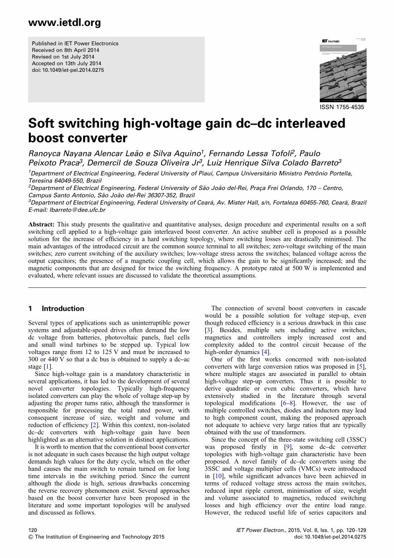
are voltages across capacitors Cr1, Cr2r, Cr3 and Cr4; VS1,VS2, VSa1 and VSa2 are voltages across switches S1, S2, Sa1and Sa2; IS1, IS2, ISa1 and ISa2 are currents through switchesS1, S2, Sa1 and Sa2; and ILr1 and ILr2 are currents throughinductors Lr1 and Lr2.First stage [t0, t1] (Fig. 2a): Initially, switch S1 and diode
D3 are on, while energy is stored in inductor Lb1 and voltagesVCr1 and VCr2 are null. This stage effectively begins when Sa2and Dr2 are turned on in ZCS condition because of inductorLr2. The current through the resonant inductor increaseslinearly from null to ILb2, so that Db2 is turned off in ZCSmode. This stage finishes when ILr2 = ILb2.Second stage [t1, t2] (Fig. 2a): This stage begins when the
current through Lr2 equals that through Lb2. Resonance occursbetween capacitors Cr3, Cr4 and inductor Lr2, causing Cr3 tobe discharged and Cr4 to be charged. The stage finisheswhen the voltage across Cr3 is null.Third stage [t2, t3] (Fig. 2b): During this stage, resonance
occurs only between Cr4 and Lr2, what occurs until currentILr2 becomes null. Besides, switch S2 is turned on in ZVScondition.Fourth stage [t3, t4] (Fig. 2b): Since current ILr2 is null,
switch Sa2 can be turned off in ZCS condition. Switches S1and S2 remain on and energy is still stored in Lb1 while Lb2is discharged. Besides, resonant capacitor Cr4 is linearlydischarged. This stage finishes when the voltage across Cr4
is null.
122& The Institution of Engineering and Technology 2015
Fifth stage [t4, t5] (Fig. 2c): When capacitor Cr4 isdischarged, diode D4 is forward biased. The input sourceVin also provides energy to inductors Lb1 and Lb2. Thisstage finishes when S1 is turned off under ZVS condition.Sixth stage [t5, t6] (Fig. 2c): After switch S1 is turned off,
capacitor Cr1 is charged by current ILb1 until the voltageacross it equals VCF. Thus diode D3 is reverse biased inZVS mode, as this stage finishes when diode Db1 is turnedon in ZVS condition.Seventh stage [t6, t7] (Fig. 2d): During this stage, the
current flows through Db1 and the energy stored in Lb1 istransferred to capacitor CF2.
3 Design procedure
3.1 Preliminary analysis and static gain
This session is concerned with the accurate design of theelements of the resonant cell shown in Fig. 1a. For thispurpose, some parametric definitions must be defined sothat the final expressions for the design of the involvedelements are represented in a more simplified form.Firstly, let us define Xa and Xb as the ratios between the
resonant capacitors, which affect the static gain and thecurrent stress across the semiconductor elements
Cr2 = Xa · Cr1 (1)
Cr4 = Xb · Cr3 (2)
Besides, the resonant capacitors can be associated so thatequivalent capacitors Cra and Crb are given as
1
Cra= 1
Cr1+ 1
Cr2(3)
1
Crb= 1
Cr3+ 1
Cr4(4)
By manipulating the previous equations, it is possible to write
Cr2 = Xa + 1( ) · Cra (5)
Cr4 = Xb + 1( ) · Crb (6)
The angular switching frequency ωs and angular resonancefrequency ωo are
vs = 2 · p · fs (7)
vo = 2 · p · fo (8)
where fs is the switching frequency and fo is the resonancefrequency. It is worth to mention that fo is a characteristicthat defines the behaviour of the active snubber, while thefollowing angular resonance frequencies can be defined
voa =1���������
Lr1 · Cra
√ (9)
voa1 =1���������
Lr1 · Cr1
√ (10)
IET Power Electron., 2015, Vol. 8, Iss. 1, pp. 120–129doi: 10.1049/iet-pel.2014.0275
Fig. 2 Operating stages of the proposed converter
a First stage and second stageb Third stage and fourth stagec Fifth stage and sixth staged Seventh stage
www.ietdl.org
voa2 =1���������
Lr1 · Cr2
√ (11)
vob =1���������
Lr2 · Crb
√ (12)
vob1 =1���������
Lr2 · Cr3
√ (13)
IET Power Electron., 2015, Vol. 8, Iss. 1, pp. 120–129doi: 10.1049/iet-pel.2014.0275
vob2 =1���������
Lr2 · Cr4
√ (14)
The resonant circuit impedance is a parameter which dependson the resonant inductor and the resonant capacitor of eachcell and also affects the soft switching characteristic of thesemiconductor elements, that is
Zoa =����Lr1Cra
√(15)
123& The Institution of Engineering and Technology 2015

Fig. 3 Main theoretical waveforms
www.ietdl.org
Zoa1 =����Lr1Cr1
√(16)
Zoa2 =����Lr1Cr2
√(17)
Zob =����Lr2Crb
√(18)
Zob1 =����Lr2Cr3
√(19)
Zob2 =����Lr2Cr4
√(20)
The normalised currents involving the snubber componentsare represented by
aa =IinVCF
·����Lr1Cra
√(21)
aa1 =IinVCF
·����Lr1Cr1
√(22)
124& The Institution of Engineering and Technology 2015
aa2 =IinVCF
·����Lr1Cr2
√(23)
ab =IinVCF
·����Lr2Crb
√(24)
ab1 =IinVCF
·����Lr2Cr3
√(25)
ab2 =IinVCF
·����Lr2Cr4
√(26)
where Iin is the input current.The ratio between the switching frequency and the
resonance frequency affects the behaviour of the snubbercell directly and must be defined as
K1 =fsfo
(27)
Parameter K corresponds to a normalised representationinvolving the resonant inductor and the resonant capacitorand is used to simplify both the calculations andrepresentation of expressions, being defined as
K = −ab
2·
��������Xb − 1
Xb + 1
√+
��������������������1
Xb− a2
b
4 · Xb + 1( )
√( )(28)
3.2 Static gains of the hard switching and softswitching converters
It is necessary to analyse the influence of the active snubberproposed in Fig. 1a in the static gain of the hard switchingversion of the converter in Fig. 1b. The thoroughmathematical procedure that leads to the resulting staticgain expression will not be discussed in detail in this paper,but it can be demonstrated
G = Vo
Vin= Iin
Io= 2 · n+ 1
1− D(29)
where n is the turns ratio of the coupled inductors in Fig. 1bdefined as (30), Vo is the output voltage, Io is the outputcurrent and D is the duty cycle
n =����Lb1L1
√=
����Lb2L2
√(30)
To determine the expression for the static gain of the softswitching converter shown in Fig. 1b, it is necessary toknow the equivalent circuits that define the converteroperation and also their respective time intervals, which arepart of the switching period Ts. From analyses of Figs. 2and Fig. 3, it is possible to determine time intervals ΔT1,
IET Power Electron., 2015, Vol. 8, Iss. 1, pp. 120–129doi: 10.1049/iet-pel.2014.0275

Fig. 4 Static gain of the interleaved boost converters
a Comparison between static gain curves of the hard and soft switchingtopologiesb Comparison between the theoretical curve of the static gain and the oneobtained with SPICE software
Fig. 5 State plane of the soft switching converter
a First state planeb Second state plane
www.ietdl.org
…, ΔT7 for the first seven operating stages
DT1 = t1 − t0 =ab
vob· 1
2 · 2 · n+ 1( ) (31)
DT2 = t2 − t1 =1
vob· acos · − 1
Xb
( )(32)
DT3 = t3 − t2 =��������Xb + 1
√vob
· acos K( ) (33)
DT4 = t4 − t3
= 2 · Xb + 1( )
Xb · ab · vob·
����������������������Xb − 1( ) · 1− K2
( )√+ K
( )(34)
DT5 = t5 − t4 = − 1
2+ D
( )· Ts − DT3 − DT4 (35)
G = 2 · n1− D+ (K1/2p) · ab/(2 · (4 · n+ 2))
( )+ aco[{
IET Power Electron., 2015, Vol. 8, Iss. 1, pp. 120–129doi: 10.1049/iet-pel.2014.0275
DT6 = t6 − t5 =2 · (2 · n+ 1) · Xa + 1
( )Xa · aa · voa
(36)
DT7 =Ts2− DT1 − DT2 − DT3 − DT4 − DT5 − DT6 (37)
It is also worth to mention that expressions for the timeintervals of the remaining stages are analogous to the onesgiven in (31)–(37).By manipulating the some equations, the static gain for the
proposed topology shown in Fig. 1b can be obtained as(see (38))
It is possible to plot expressions (29) and (38) as in Fig. 4a.Even though the static gain expression of the soft switchingconverter depends on parameters that characterise thebehaviour of the snubber, that is, K1, αb and Xb, it can beseen that the adopted cell does not influence the static gainof the hard switching topology significantly.To validate the theoretical expression of the static gain
given by (38), simulation tests were carried out insimulation program with integrated circuit emphasis(SPICE) related software using realistic models ofsemiconductor components provided by the application.Components Db1 and Db2 correspond to ultrafast diodesHFA25PB60 by International Rectifier; Dr1, Dr2, D1, D2, D3
and D4 are ultrafast diodes MUR460 by ON semiconductor;and the main switches and auxiliary switches are Metaloxide semiconductor field effect transistors IRFP4710 byInternational Rectifier. It is also worth to mention that theaforementioned semiconductor elements are the same onesused in the implementation of the experimental prototype.The static gain plot is obtained considering n = 1 as defined
in (30), while the duty cycle is varied from 0.1 to 0.9 in thesimulation. Fig. 4b shows the obtained curve comparedwith the one given by expression (38), thus validating thetheoretical assumption for the soft switching converter.
3.3 Condition for the achievement of softswitching
Considering a single snubber cell represented by Fig. 1a, it ispossible to note that there are two distinct resonance
+ 1
s −(1/Xb)( )+ (4 · n+ 2)(Xb + 1)
( )/ Xb · ab
( )]} (38)
125& The Institution of Engineering and Technology 2015

Table 1 Design specifications for the step-up converters
Parameters Specifications
rated input voltage Vi = 28 Voutput power Po = 500 Woutput voltage Vo = 180 Vswitching frequency fs = 50 kHzestimated theoreticalefficiency
η = 90%
Designed elementsinductors L1, L2, Lb1, Lb2 L1 = L2 = Lb1 = Lb2 = 220 μH, core NEE
65/33/26 by Thornton, 20 turns, 6 ×Amerícan wire gauge (AWG) 19
resonant capacitors Cr1 =Cr3 = 27 nF, Cr2 =Cr4 = 100 nFresonant inductors Lr1 = Lr2 = 0.5 μH, core NEE 20/10/5 by
Thornton, 2 turns, 12 × AWG 22capacitors CF1, CF2, CF CF1 =CF2 =CF = 680 μF/250 Vdiodes Db1, Db2 HFA25PB60diodes Dr1, Dr2, D1, D2,D3, D4
MUR460
switches S1, S2, Sa1, Sa2 IRFP4710
Fig. 6 Experimental prototype
www.ietdl.org
frequencies, which are given by expressions (10) and (11),since there are two resonant capacitors and one resonantinductor. The state plane of the converter can then bedivided into two plots, as shown in Fig. 5.From the analysis of Fig. 5a, the following inequality can
be obtained
Xb ≥ 1 (39)
Analogously from Fig. 5b, it is possible to obtain thefollowing expression
Xb ≤1
4 · a2b2
+ 1 (40)
It is then possible to state that the restrictions given in (39) and(40) must be obeyed so that the soft switching characteristicof the snubber cell is maintained.
3.4 Stresses regarding the semiconductorelements
The addition of the soft switching cell to the power converterinvolves the determination of the current and voltage stressesregarding the semiconductor elements. From the operating
IDb2 avg( )Iin
= 1
4 · n+ 2( ) 1− D− K1
2 · p · ab
2 · 4 · n([{
IDb2 rms( )Iin
= 1
4 · n+ 2( ) · 1− D− K1
2 · p · ab
4 · n+ 2( ) + acos −([{{
ISa2 avg( )Iin
= K1
2 · pab
2· 1
2 · 2 · n+ 1( )[ ]2 +1
2· arccos − 1
Xb
( )+ �
X√{
126& The Institution of Engineering and Technology 2015
stages and theoretical waveforms, it is possible to properlydesign the diodes and switches used in the converter shownin Fig. 1b.The normalised average current, normalised root mean
square (rms) current, normalised maximum current andmaximum voltage regarding diode Db2 are given byexpressions (41)–(45), respectively. It can be seen that thecurrent stresses depend on parameters that define thebehaviour of the snubber, for example,. expressions (2) and(24) (see (41 and 42))
IDb2 max( )Iin
= 1
2 · 2 · n+ 1( ) (43)
VDb2 max( ) = VCF + VCr4 (44)
The normalised average current, normalised rms current,normalised maximum current and maximum voltageregarding auxiliary switch Sa2 and auxiliary diode Dr2 aregiven by expressions (45)–(48), respectively (see (45 and46 at the bottom of the next page))
ISa2(max )
Iin= ab + 2
2 · ab(47)
VSa2(max ) = VCF (48)
The normalised average current, normalised rms current,normalised maximum current and maximum voltageregarding main switch S2 are given by expressions (49)–
+ 2) + acos−1
Xb
( )+ 4 · n+ 2( ) · Xb + 1
( )Xb · ab
]}(41)
1
Xb
)+ 4 · n+ 2( ) · Xb + 1
( )Xb · ab
− ab
3 · 4 · n+ 2( )2]}}1
2 (42)
�������b + 1 · arccos K( ) + Xb + 1
Xb · ab·
����������������������Xb − 1( ) · 1− K2
( )√+ K
][ }(45)
IET Power Electron., 2015, Vol. 8, Iss. 1, pp. 120–129doi: 10.1049/iet-pel.2014.0275

Fig. 7 Experímental results
a Input current and input voltageb Output current and output voltagec Voltages across the output capacitorsd Current and voltage waveforms of main switch S1
www.ietdl.org
(52), respectively (see (50))
IS2 avg( )Iin
= − 1
2+ D+ 1− D( ) · 1− 1
2 · 2 · n+ 1( )( )
− 1
2· K1
2 · p · ��������Xb + 1
√ · arccos K( ) (49)
ISa2 rms( )Iin
= K1
2 · p · 1
2 · (2 · n+ 1)[ ]3 · ab
3+ 1
4· acos − 1
Xb
( )+
⎧⎨⎩
⎧⎨⎩+ 1
4· ��������
Xb + 1√ · acos(K)+ 1
ab· Xb + 1( )
Xb·
��������Xb + 1(√[
+��������Xb + 1
√a2b
· Xb + 1( )
X 2b
· Xb
2arccos K( ) +
��������1− K2
√·
([
IS2 rms( )Iin
= − 1
2+ D+ 1− D( ) · 1− 1
2 · 2 · n(([
IET Power Electron., 2015, Vol. 8, Iss. 1, pp. 120–129doi: 10.1049/iet-pel.2014.0275
IS2 max( )Iin
= 1− 1
2 · (2 · n+ 1)(51)
VS2 max( ) = VCF (52)
The normalised average current, normalised rms current,normalised maximum current and maximum voltage
1
ab· Xb + 1
Xb
( )+ 1
2 · a2b
· acos − 1
Xb
( )+
��������X 2b + 1
X 4b
√⎡⎣
⎤⎦
��������������) · 1− K2( )+ K − 1
]
K)− ��������
Xb − 1√ ·
��������1− K2
√ ]⎫⎬⎭⎫⎬⎭
1/2
(46)
+ 1))− 1
2· K1
2 · p · ��������Xb + 1
√ · arccos K( )]1/2
(50)
127& The Institution of Engineering and Technology 2015
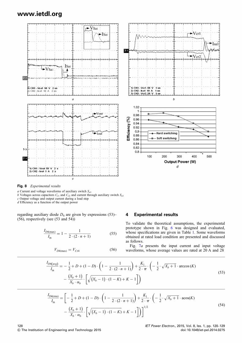
Fig. 8 Experimental results
a Current and voltage waveforms of auxiliary switch Sa1b Voltages across capacitors Cr1 and Cr2 and current through auxiliary switch Sa1c Output voltage and output current during a load stepd Efficiency as a function of the output power
www.ietdl.org
regarding auxiliary diode D4 are given by expressions (53)–(56), respectively (see (53 and 54))
ID4 max( )Iin
= 1− 1
2 · 2 · n+ 1( ) (55)
VD4 max( ) = VCr4 (56)
ID4 avg( )Iin
= − 1
2+ D+ (1− D) · 1− 1
2 · (2 · n+(
− Xb + 1( )Xb · ab
·��������������������Xb − 1( ) · (1− K)
√+
[
ID4 rms( )Iin
= − 1
2+ D+ (1− D) · 1− 1
2 · (2 · n([
− Xb + 1( )Xb · ab
·��������������������Xb − 1( ) · (1− K)
√+
[
128& The Institution of Engineering and Technology 2015
4 Experimental results
To validate the theoretical assumptions, the experimentalprototype shown in Fig. 6 was designed and evaluated,whose specifications are given in Table 1. Some waveformsobtained at rated load condition are presented and discussedas follows.Fig. 7a presents the input current and input voltage
waveforms, whose average values are rated at 20 A and 28
1)
)+ K1
2 · p · − 1
2· ��������
Xb + 1√ · arccos (K)
(
K − 1
]) (53)
+ 1)
)+ K1
2 · p · − 1
2· ��������
Xb + 1√ · acos(K)
(
K − 1
])]1/2 (54)
IET Power Electron., 2015, Vol. 8, Iss. 1, pp. 120–129doi: 10.1049/iet-pel.2014.0275

www.ietdl.org
V, respectively. Besides, the average output current andoutput voltage are shown in Fig. 7b, which are about 2.78A and 180 V, respectively.Fig. 7c presents the waveforms regarding the outputcapacitors, where it can be seen that the voltages across CF1
and CF2 are balanced, although there is a slight differencein the voltage across CF. It occurs because VCF1 and VCF2
depend on the turns ratio and leakage inductance of theinductors, whereas VCF depends only on the duty cycle.According to Fig. 7d, it can be seen that ZVS turn on
occurs for main switch S1, whereas ZCS turn on is verifiedin the waveforms shown in Fig. 8a for auxiliary switch Sa1.Switching losses are then drastically reduced if comparedwith the hard switching version of the topology in Fig. 1b.The waveforms regarding the resonant capacitors Cr1 and Cr2
and auxiliary switch Sa1 are represented in Fig. 8b, which aresimilar to those predicted in the theoretical analysis and areanalogous to those regarding capacitors Cr1, Cr2 and Sa1.The behaviour of the output voltage during positive and
negative load steps is presented in Fig. 8c, where it can beseen that the converter operation is stable. It is worth tomention that the design of the control system is based onthe transfer function of the output voltage to the duty cycle,which is the same as that of the classical boost converter.Therefore the detailed design procedure of the controlsystem will not be presented in this paper.Finally, the efficiency curves of the hard switching (without the
use of the snubber cell shown in Fig. 1a) and soft switchingtopologies are shown in Fig. 8d, where the same operatingconditions are assumed to establish a fair comparison. Theefficiency of the proposed converter is significantly higher thanthat achieved by the original topology over the entire loadrange. The difference may be up to 4% when the converter isevaluated from light load to heavy load conditions.
5 Conclusions
This paper has presented the qualitative analysis, operatingprinciple, theoretical waveforms and experimental results onan active soft switching cell applied to a high-voltage gaininterleaved boost converter. It has been shown that theactive switches present ZVS commutation, whereas theauxiliary switches operate under ZCS condition, thusleading to the significant reduction of switching losses.The theoretical analysis has demonstrated that the static
gain of the original topology remains practically unaffectedwhen the snubber is added. Good voltage balance involvingthe output capacitors is also achieved, with a slightunbalance involving capacitors CF1–CF2 and CF.The most significant advantage of the proposed converter
lies in the increased efficiency if compared with the hardswitching topology because of the significant reduction ofswitching losses. At rated load, it has been shown theefficiencies for the original converter and the soft switchingone are 87.67 and 91%, respectively. Even though highcomponent count and some complexity can be addressed tothe arrangement, its application becomes interesting athigh-current high-power applications where the switchingfrequency and power levels may become high enough tocompromise the overall efficiency.
6 References
1 Bascopé, R.P.T., Branco, C.G.C., Bascopé, G.V.T., Cruz, C.M.T., deSouza, F.A.A., Barreto, L.H.S.C.: ‘A new isolated dc-dc boost
IET Power Electron., 2015, Vol. 8, Iss. 1, pp. 120–129doi: 10.1049/iet-pel.2014.0275
converter using three-state switching cell’. Proc. Applied PowerElectronics Conf. and Exposition, 2008, pp. 607–613
2 Barreto, L.H.S.C., Peixoto Praca, P., Oliveira, D.S., Silva, R.N.A.L.:‘High-voltage gain boost converter based on three-state commutationcell for battery charging using PV panels in a single conversionstage’, IEEE Trans. Power Electron., 2014, 29, (1), pp. 150–158
3 Demian Jr., A.E., Treviso, C.H.G., Gallo, C.A., Tofoli, F.L.:‘Non-isolated dc–dc converters with wide conversion range used todrive high-brightness LED’. Proc. Brazilian Power Electronics Conf.,2009, pp. 598–605
4 Vighetti, S., Ferrieux, J., Lembeye, Y.: ‘Optimization and design of acascaded dc/dc converter devoted to grid-connected photovoltaicsystems’, IEEE Trans. Power Electron., 2012, 27, (4), pp. 2018–2027
5 Middlebrook, R.D.: ‘Transformerless dc-to-dc converters with largeconversion ratios’, IEEE Trans. Power Electron., 1988, 3, (4), pp. 484–488
6 Novaes, Y.R., Rufer, A., Barbi, I.: ‘A new quadratic, three-level, dc/dcconverter suitable for fuel cell applications’. Proc. Power ConversionConf. – Nagoya, 2007, pp. 601–607
7 Lopez-Santos, O., Martinez-Salamero, L., Garcia, G., Valderrama-Blavi,H., Mercuri, D.O.: ‘Efficiency analysis of a sliding-mode controlledquadratic boost converter’, IET Power Electron., 2013, 6, (12),pp. 364–373
8 Chen, S.-M., Liang, T.-J., Yang, L.-S., Chen, J.-F.: ‘A cascaded highstep-up dc–dc converter with single switch for microsourceapplications’, IEEE Trans. Power Electron., 2011, 26, (4),pp. 1146–1153
9 Torrico-Bascopé, G.V., Barbi, I.: ‘Generation of a family of non-isolatedDC-DC PWM converters using new three-state switching cell’. Proc.IEEE Power Electronics Specialists Conf., 2000, vol. 2, pp. 858–863
10 Tofoli, F.L., Oliveira Jr., D.S., Torrico-Bascopé, R.P., Alcazar, Y.J.A.:‘Novel nonisolated high-voltage gain dc–dc converters based on 3SSCand VMC’, IEEE Trans. Power Electron., 2013, 27, (9), pp. 3897–3907
11 Bascopé, G.V.T., Bascopé, R.P.T., Oliveira, Jr., D.S., Antunes, F.L.M.,Araújo, S.V., Branco, C.G.C.: ‘A high step-up dc-dc converter based onthree-state switching cell’. Proc. IEEE Int. Symp. on IndustrialElectronics, 2006, pp. 998–1003
12 Li, W., He, X.: ‘Review of nonisolated high-step-up dc/dc converters inphotovoltaic grid-connected applications’, IEEE Trans. Ind. Electron.,2011, 58, (4), pp. 1239–1250
13 Hu, X., Gong, C.: ‘A high voltage gain dc–dc converter integratingcoupled-inductor and diode–capacitor techniques’, IEEE Trans. PowerElectron., 2014, 29, (2), pp. 789–800
14 Hsieh, Y.-P., Chen, J.-F., Yang, L.-S., Wu, C.-Y., Liu, W.-S.:‘High-conversion-ratio bidirectional dc–dc converter with coupledinductor’, IEEE Trans. Ind. Electron., 2014, 61, (1), pp. 210–222
15 Zhao, Q., Lee, F.C.: ‘High-efficiency, high step-up dc–dc converters’,IEEE Trans. Power Electron., 2003, 18, (1), pp. 65–73
16 Barreto, L.H.S.C., Coelho, E.A.A., Farias, V.J., Oliveira, J.C., deFreitas, L.C., Vieira Jr., J.B.: ‘A quasi-resonant quadratic boostconverter using a single resonant network’, IEEE Trans. Ind.Electron., 2005, 52, (2), pp. 552–557
17 Jang, Y., Jovanovic, M.M.: ‘Interleaved boost converter with intrinsicvoltage-doubler characteristic for universal-line PFC front end’, IEEETrans. Power Electron., 2007, 22, (4), pp. 1394–1401
18 Yungtaek, J., Jovanovic, M.M.: ‘New two-inductor boost converter withauxiliary transformer’, IEEE Trans. Power Electron., 2004, 19, (1),pp. 169–175
19 Gules, R., Pfitscher, L.L., Franco, L.C.: ‘An interleaved boost dc-dcconverter with large conversion ratio’. Proc. IEEE Int. Symp. onIndustrial Electronics, 2003, pp. 411–416
20 Silva, E.A.S., Oliveira Jr., D.S., Oliveira, T.A.M., Tofoli, F.L.: ‘A novelinterleaved boost converter with high voltage gain for UPS applications’.Proc. Brazilian Power Electronics Conf., 2007, pp. 999–1003
21 Mishima, T., Takeuchi, Y., Nakaoka, M.: ‘Analysis, design, andperformance evaluations of an edge-resonant switched capacitorcell-assisted soft-switching PWM boost dc–dc converter and itsinterleaved topology’, IEEE Trans. Power Electron., 2013, 28, (7),pp. 3363–3378
22 Wu, T.-F., Yang, J.-G., Kuo, C.-L., Wu, Y.-C.: ‘Soft-switchingbidirectional isolated full-bridge converter with active and passivesnubbers’, IEEE Trans. Ind. Electron., 2014, 61, (3), pp. 1368–1376
23 Hu, B., Sathiakumar, S.: ‘Interleaving technique of series connectedmodule-integrated converters for PV systems: novel approach andsystem analysis’. Proc. IEEE Int. Symp. on Industrial Electronics(ISIE), 2012, pp. 1785–1790
24 Li, W., He, X.: ‘ZVT interleaved boost converters for high-efficiency,high-step-up DC/DC conversion’, IET Electr. Power Appl., 2007, 1,(2), pp. 284–290
25 Wai, R.J., Duan, R.Y.: ‘High-efficiency dc/dc converter with highvoltage gain’, IET-Electr. Power Appl., 2005, 152, (4), pp. 793–802
129& The Institution of Engineering and Technology 2015