institut de science des matériaux de mulhouse (is2m)€¦ · 1 calculs multi-échelles de la...
TRANSCRIPT
1
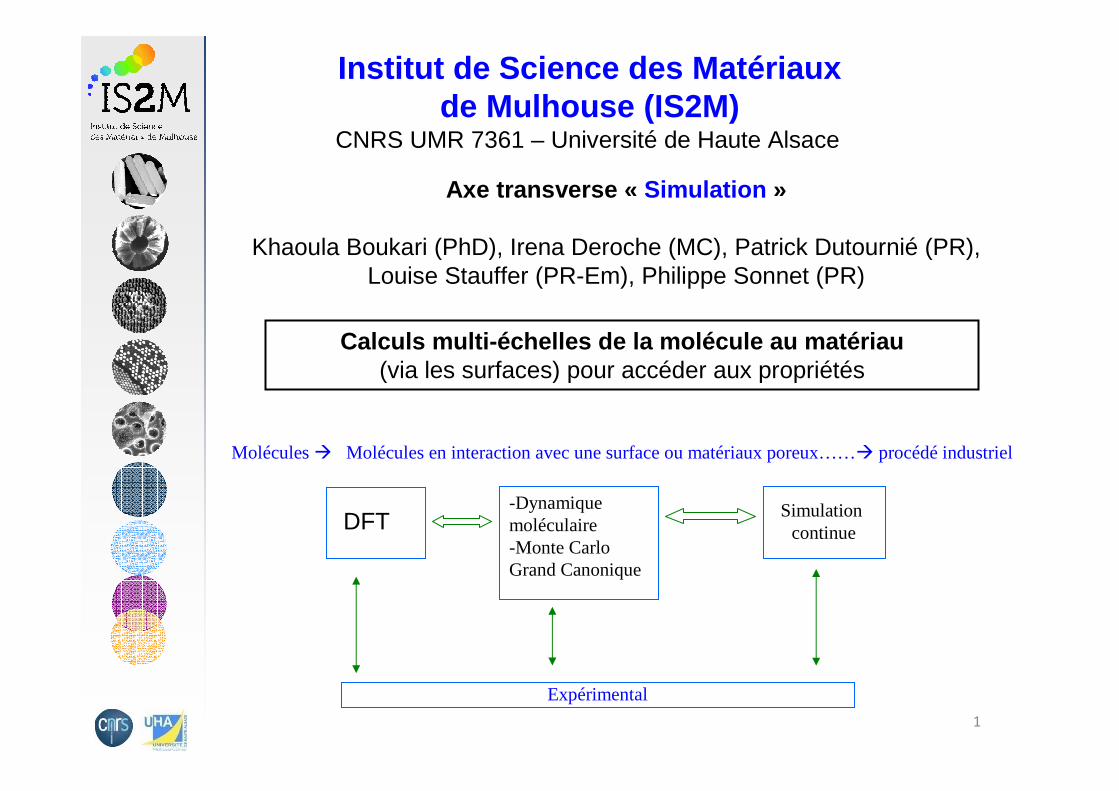
Calculs multi-échelles de la molécule au matériau(via les surfaces) pour accéder aux propriétés
Institut de Science des Matériaux de Mulhouse (IS2M)
CNRS UMR 7361 – Université de Haute Alsace
Axe transverse « Simulation »
Khaoula Boukari (PhD), Irena Deroche (MC), Patrick Dutournié (PR), Louise Stauffer (PR-Em), Philippe Sonnet (PR)
Molécules � Molécules en interaction avec une surface ou matériaux poreux……� procédé industriel
Expérimental
DFT-Dynamique moléculaire-Monte Carlo Grand Canonique
Simulation continue
2
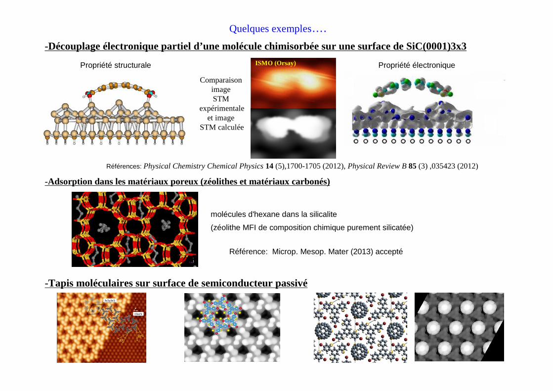
Quelques exemples….
-Découplage électronique partiel d’une molécule chimisorbée sur une surface de SiC(0001)3x3
Comparaison image STM
expérimentaleet image
STM calculée
ISMO (Orsay)
-Tapis moléculaires sur surface de semiconducteur passivé
-Adsorption dans les matériaux poreux (zéolithes et matériaux carbonés)
Propriété structurale Propriété électronique
Références: Physical Chemistry Chemical Physics 14 (5),1700-1705 (2012), Physical Review B 85 (3) ,035423 (2012)
Référence: Microp. Mesop. Mater (2013) accepté
molécules d'hexane dans la silicalite
(zéolithe MFI de composition chimique purement silicatée)
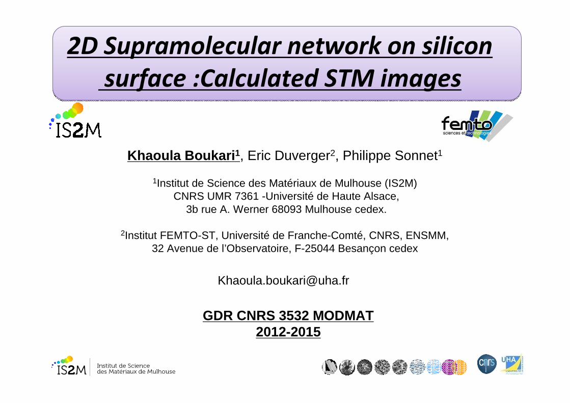
2D Supramolecular network on silicon
surface :Calculated STM images
Khaoula Boukari 1, Eric Duverger2, Philippe Sonnet1
1Institut de Science des Matériaux de Mulhouse (IS2M)CNRS UMR 7361 -Université de Haute Alsace,
3b rue A. Werner 68093 Mulhouse cedex.
2Institut FEMTO-ST, Université de Franche-Comté, CNRS, ENSMM, 32 Avenue de l’Observatoire, F-25044 Besançon cedex
3
GDR CNRS 3532 MODMAT2012-2015
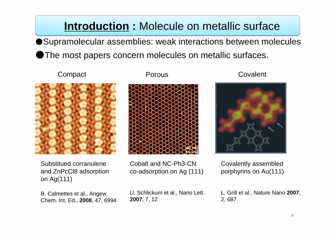
●Supramolecular assemblies: weak interactions between molecules
●The most papers concern molecules on metallic surfaces.
Substitued corranuleneand ZnPcCl8 adsorptionon Ag(111)
B. Calmettes et al., Angew. Chem. Int. Ed., 2008, 47, 6994
Cobalt and NC-Ph3-CN co-adsorption on Ag (111)
U. Schlickum et al., Nano Lett. 2007, 7, 12
Covalently assembled porphyrins on Au(111)
L. Grill et al., Nature Nano 2007,2, 687
4
Introduction : Molecule on metallic surface
Compact Porous Covalent
Strong surface-molecules interactions
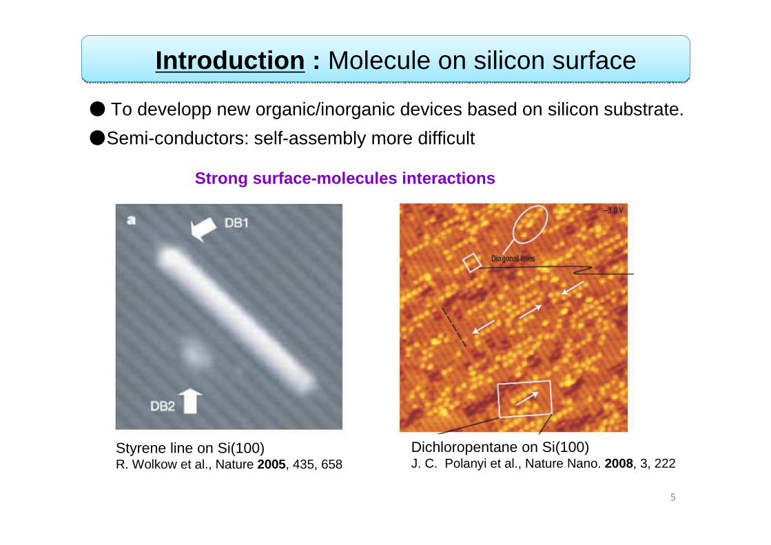
●Semi-conductors: self-assembly more difficult
Styrene line on Si(100) R. Wolkow et al., Nature 2005, 435, 658
5
Introduction : Molecule on silicon surface
● To developp new organic/inorganic devices based on silicon substrate.
Dichloropentane on Si(100)J. C. Polanyi et al., Nature Nano. 2008, 3, 222

6
Introduction : The Si (111)-B substrate
Weak reactivity of Si-adatoms
e-
√3x√3R30°
7.5 x 8.0 nm2, Vs = 1.8 V, It = 0.04 nA, RT
Boron defect
Undoped Si(111) Boron doped Si(111)
Populated DB Depopulated DB

TBB on HOPG and Cu(111)R. Gutzler et al. Chem. Commun., 2009, 4456 7
TBB network: 1,3,5-tri(4’-bromophenyl)benzene
● Covalent assembly after annealing on Cu(111)
●Supramolecular network on HOPG
C atoms
H atoms
Br atoms
Compact Porous
8
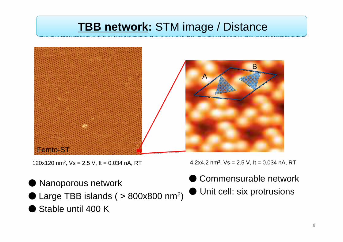
120x120 nm2, Vs = 2.5 V, It = 0.034 nA, RT
● Nanoporous network
● Large TBB islands ( > 800x800 nm2) ● Stable until 400 K
● Commensurable network● Unit cell: six protrusions
TBB network: STM image / Distance
B
AB
4.2x4.2 nm2, Vs = 2.5 V, It = 0.034 nA, RT
Femto-ST
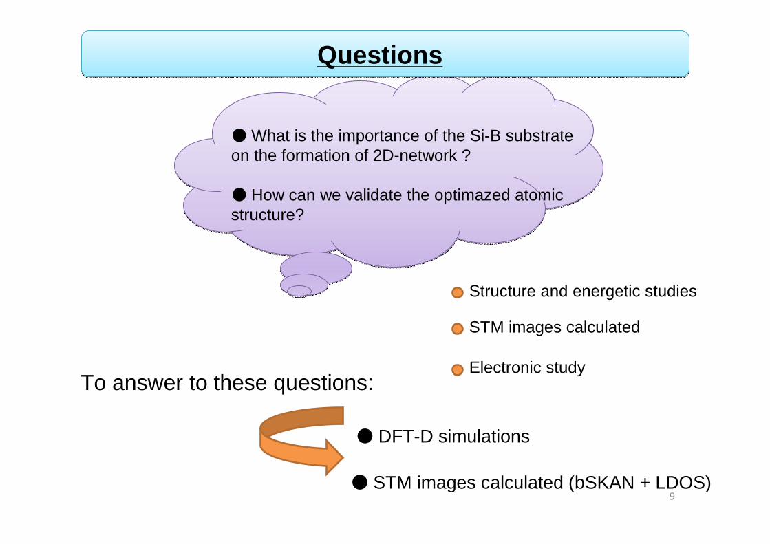
● DFT-D simulations
To answer to these questions:
●What is the importance of the Si-B substrate on the formation of 2D-network ?
● How can we validate the optimazed atomic structure?
9
Questions
● STM images calculated (bSKAN + LDOS)
Structure and energetic studies
STM images calculated
Electronic study
10
Methods
*
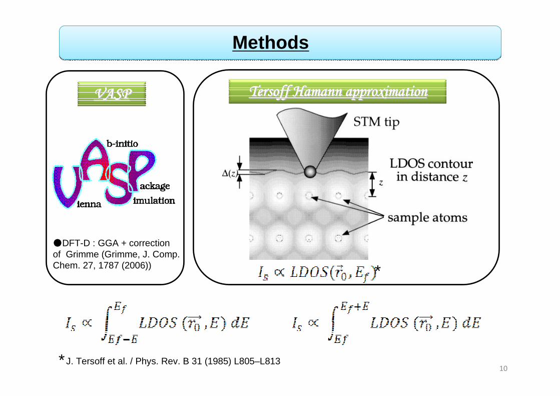
●DFT-D : GGA + correction of Grimme (Grimme, J. Comp. Chem. 27, 1787 (2006))
VASPVASPVASPVASPVASPVASPVASPVASP Tersoff Hamann approximation Tersoff Hamann approximation Tersoff Hamann approximation Tersoff Hamann approximation Tersoff Hamann approximation Tersoff Hamann approximation Tersoff Hamann approximation Tersoff Hamann approximation
*
J. Tersoff et al. / Phys. Rev. B 31 (1985) L805–L813

1111
Methods
χχ ψψBSKANBSKAN
Bias voltageSTM tip model
Surface
DFTvasp
DFTvasp
Current tunnellingis calculated
bSKANbSKANbSKANbSKANbSKANbSKANbSKANbSKAN
Materials Modelling, DL, March 20,2007W.A. Hofer et al. / Surface Science 405 (1998) L514–L519
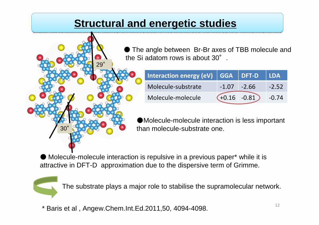
●Molecule-molecule interaction is less important than molecule-substrate one.
●Molecule-molecule interaction is repulsive in a previous paper* while it is attractive in DFT-D approximation due to the dispersive term of Grimme.
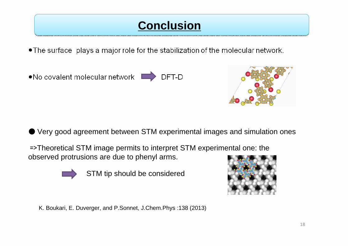
The substrate plays a major role to stabilise the supramolecular network.
12
Structural and energetic studies
29°
30°
● The angle between Br-Br axes of TBB molecule and the Si adatom rows is about 30°.
* Baris et al , Angew.Chem.Int.Ed.2011,50, 4094-4098.
Interaction energy (eV) GGA DFT-D LDA
Molecule-substrate -1.07 -2.66 -2.52
Molecule-molecule +0.16 -0.81 -0.74
13
Structural and energetic studies
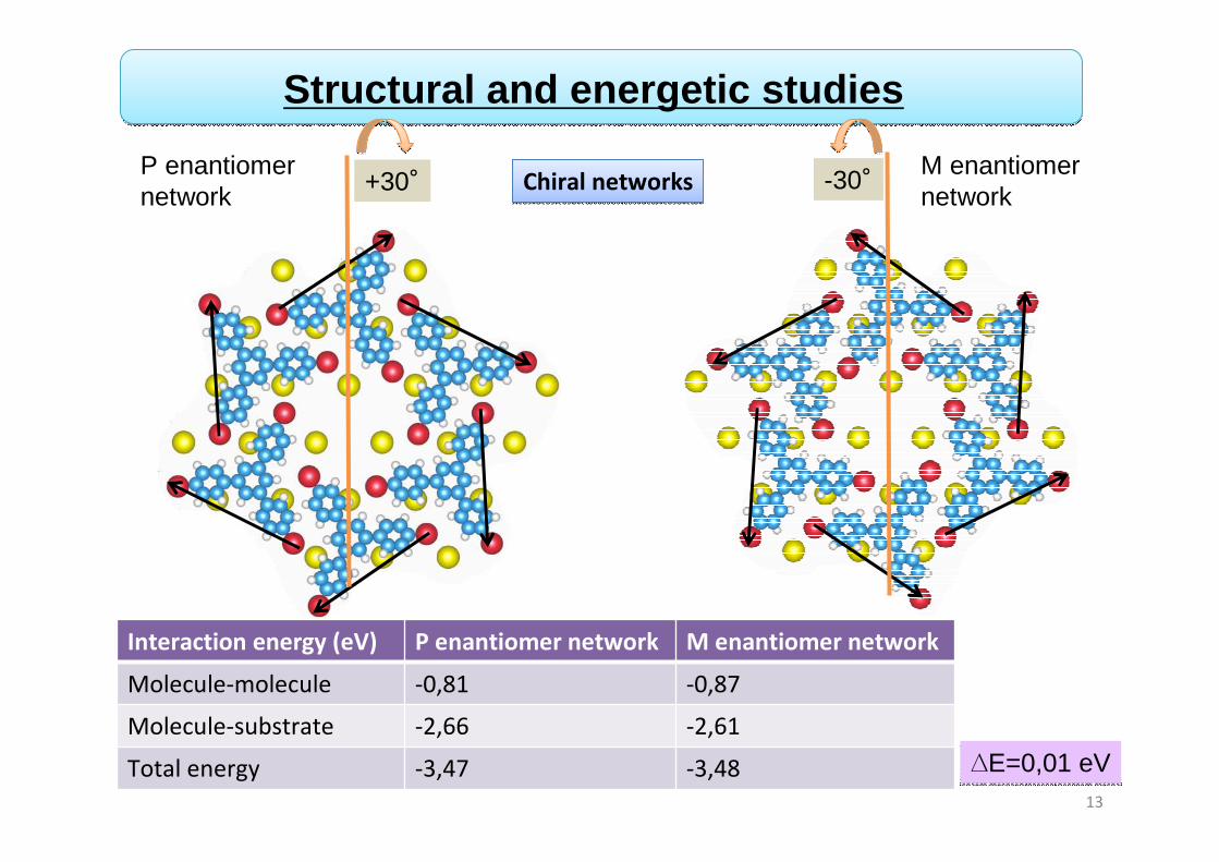
+30° -30°Chiral networksChiral networks
Interaction energy (eV) P enantiomer network M enantiomer network
Molecule-molecule -0,81 -0,87
Molecule-substrate -2,66 -2,61
Total energy -3,47 -3,48 ∆E=0,01 eV∆E=0,01 eV
P enantiomer network
M enantiomer network

14
LDOS Calculated image with smoothing
STM experimental image
14
STM / LDOS/ bSKAN image
LDOS Calculated image without smoothing
Femto-ST Vs= 2.5 V
E=+ 2.5 eV
E= + 2.5 eV
Vs= 2.5 V
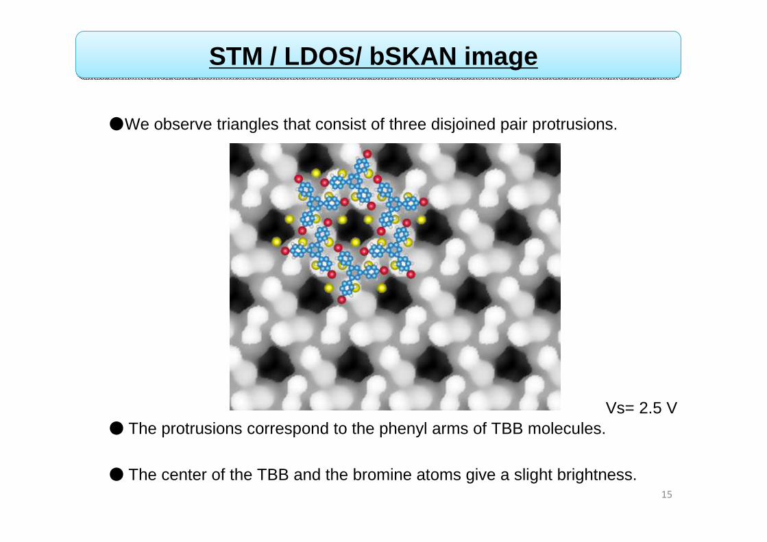
●We observe triangles that consist of three disjoined pair protrusions.
● The protrusions correspond to the phenyl arms of TBB molecules.
15
STM / LDOS/ bSKAN image
● The center of the TBB and the bromine atoms give a slight brightness.
Vs= 2.5 V

1616
Electronic study
Vs= 2.5 V
Bromine atoms are not visible in STM image.
Bromine elertronic states are located at -3.eV

No shared charge density between molecule-molecule and molecule-substrate : no covalent interaction
Charge density
17
Top view Side view
Unit cell
18
Conclusion
K. Boukari, E. Duverger, and P.Sonnet, J.Chem.Phys :138 (2013)
=>Theoretical STM image permits to interpret STM experimental one: theobserved protrusions are due to phenyl arms.
● Very good agreement between STM experimental images and simulation ones
STM tip should be considered

19
Thank
You
For
Attention
Your

Directional interaction between adatoms and phenyl ring
20
Electron rich phenyls interact with electron poor silicon adatoms
Charge density difference ∆∆∆∆ρρρρ
A
B
∆ρ=ρ(molecules+substrate)-ρ(molecules)-ρ(substrate)
Blue : ∆ρ>0 => eRed: ∆ρ<0 => e
Electrostatic interaction

21

22
√√√√3x√√√√3
3√√√√3x3√√√√
3

23
∆∆∆∆z (Å) DFT DFT-D
Molecule A 3,86 2,72
Molecule B 3,96 2,81