burstlink: techniques for energy-efficient conventional and
TRANSCRIPT
BurstLink: Techniques for Energy-Efficient Video Displayfor Conventional and Virtual Reality Systems
Jawad Haj-YahyaETH Zürich
Jisung ParkETH Zürich
Rahul BeraETH Zürich
Juan Gómez LunaETH Zürich
Taha ShahroodiETH Zürich, TU Delft
Jeremie S. KimETH Zürich
Efraim RotemIntel Corporation
Onur MutluETH Zürich
ABSTRACTConventional planar video streaming is the most popular applica-tion in mobile systems. The rapid growth of 360◦ video content andvirtual reality (VR) devices is accelerating the adoption of VR videostreaming. Unfortunately, video streaming consumes significantsystem energy due to high power consumption of major systemcomponents (e.g., DRAM, display interfaces, and display panel)involved in the video streaming process. For example, in conven-tional planar video streaming, the video decoder (in the processor)decodes video frames and stores them in the DRAM main memorybefore the display controller (in the processor) transfers decodedframes from DRAM to the display panel. This system architecturecauses large amount of data movement to/from DRAM as well ashigh DRAMbandwidth usage. As a result, DRAM by itself consumesmore than 30% of the video streaming energy.
We propose BurstLink, a novel system-level technique that im-proves the energy efficiency of planar and VR video streaming.BurstLink is based on two key ideas. First, BurstLink directly trans-fers a decoded video frame from the video decoder or the GPU tothe display panel, completely bypassing the host DRAM. To thisend, we extend the display panel with a double remote frame buffer(DRFB) instead of DRAM’s double frame buffer so that the systemcan directly update the DRFB with a new frame while updating thedisplay panel’s pixels with the current frame stored in the DRFB.Second, BurstLink transfers a complete decoded frame to the displaypanel in a single burst, using the maximum bandwidth of moderndisplay interfaces.
Unlike conventional systems where the frame transfer rate is lim-ited by the pixel-update throughput of the display panel, BurstLinkcan always take full advantage of the high bandwidth of moderndisplay interfaces by decoupling the frame transfer from the pixelupdate as enabled by the DRFB. This direct and burst frame transferof capability BurstLink significantly reduces energy consumptionof video display by 1) reducing accesses to DRAM, 2) increasingsystem’s residency at idle power states, and 3) enabling temporalpower gating of several system components after quickly transfer-ring each frame into the DRFB.
BurstLink can be easily implemented in modern mobile systemswith minimal changes to the video display pipeline. We evaluateBurstLink using an analytical power model that we rigorouslyvalidate on an Intel Skylake mobile system. Our evaluation showsthat BurstLink reduces system energy consumption for 4K planarand VR video streaming by 41% and 33%, respectively. BurstLinkprovides an even higher energy reduction in future video streamingsystems with higher display resolutions and/or display refresh rates.
CCS CONCEPTS•Hardware→ Platform power issues; Displays and imagers.
KEYWORDSvideo streaming, video display, display panels, energy efficiency,data movement, mobile systems, memory, DRAM
1 INTRODUCTIONConventional planar (i.e., 2-dimensional) video streaming is themost prevalent application in mobile devices [18]. Virtual reality(VR) video streaming is emerging as one of the most importantapplications in the entertainment market [117]. Cisco predicts thatvideo streaming will generate more than 79% of mobile data trafficby 2022 [22], and Goldman Sachs predicts that around 79 millionusers will use VR video streaming by 2025 [49]. To provide userswith an immersive experience, video formats and mobile displaypanels support increasingly high resolutions (e.g., 4K [6, 88]) andrefresh rates (e.g., 120Hz [89]). These trends come at the cost ofsignificantly higher energy consumption of video display, whichnegatively impacts the battery life of a mobile device [100]. Mobilesystems need an efficient planar/VR video display architecture thatprovides high energy efficiency while enabling high video/displayresolutions and refresh rates.
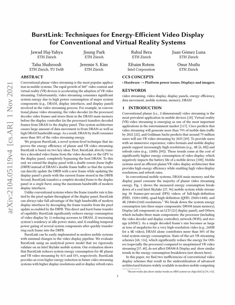
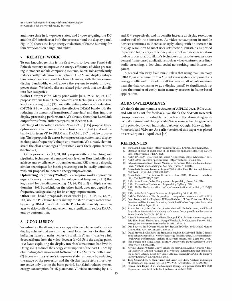
In conventional mobile systems, DRAM main memory and thedisplay panel consume the majority of planar video streamingenergy. Fig. 1 shows the measured energy consumption break-down of a real Intel Skylake [27, 96] mobile system while stream-ing 30 frames-per-second (FPS) videos of full-high-definition(FHD, 1920×1080), quad-high-definition (QHD, 2560×1440), and4K (3840×2160) resolutions.1 We break down the system energyconsumption into three major components: DRAM (main memory),Display (all components in an LCD [21] display panel), and Others,which includes three main components: the processor (includingthe video decoder and display controller), network (WiFi), and stor-age (eMMC). As a single decoded frame’s size becomes as largeas tens of megabytes for a very high-resolution video (e.g., 24MBfor a 4K video), DRAM alone contributes more than 30% of thetotal system energy consumption. State-of-the-art VR streamingschemes [68, 116], which significantly reduce the energy for Oth-ers (especially the processor) compared to unoptimized VR videostreaming [37, 48], do not affectDRAM&Display and show similartrends in the energy consumption breakdown (not shown here).
In this paper, we find two inefficiencies of conventional videodisplay schemes that result in the underutilization of advancedarchitectural features widely available in modern mobile computing
1Recent works also show similar trends on ARM system-on-chips (SoCs) [74, 113].1
arX
iv:2
104.
0511
9v4
[cs
.AR
] 1
Nov
202
1
Haj-Yahya, et al.
0%25%50%75%
100%125%150%
FHD QHD 4K
% o
f En
ergy
No
rm.
to F
HD
To
tal E
ner
gy
Display Resolutions
DRAM Display Others
Figure 1: Energy consumption of a modern mobile comput-ing system while streaming videos at various resolutions,normalized to FHD.
systems. First, the video decoder or GPU stores video frames in theDRAMmainmemory before the display controller (in the processor)transfers these frames fromDRAM to the display panel. This systemarchitecture causes large amount of data movement to/from DRAMas well as high DRAM bandwidth usage. Modern mobile systemscommonly employ a remote frame buffer (RFB) inside the displaypanel to improve energy efficiency in a static-image display (seeSection 2.3 for more details). Unfortunately, current video streamingarchitectures do not utilize the RFB due to a few limitations. Forexample, when other planes (e.g., graphical user interface (GUI) andcursor planes) must be displayed in addition to the video plane, thedisplay controller (DC) must first merge them with the video planeto generate a single frame that the DC sends to the display panel.However, when there is no interaction between the video plane andother planes, we could significantly reduce energy consumption ifwe send the decoded video frames directly to the display and bypasshost DRAM. Unfortunately, current video streaming architecturesdo not utilize this opportunity due to limitations in datapaths ofboth the processor and the display panel.
Second, conventional video processing and display schemes un-derutilize the high bandwidth provided by modern display inter-faces. The state-of-the-art embedded-DisplayPort (eDP) [103, 105]interface supports a peak bandwidth of 25.92 Gbps [105] to copewith high-quality videos with high resolutions and frame rates.However, even when displaying a 4K 60FPS video, conventionalmobile systems send each frame at a transfer rate of about 11.3Gbps. This underutilization is because the display panel’s pixel-update bandwidth dictates the frame transfer rate between the hostsystem and the display panel. The eDP-bandwidth underutiliza-tion negatively affects energy efficiency since a long time spent foractively transferring frames reduces the time that the system canspend in low-power states. This inefficiency is expected to remainfor the coming years, considering the large quality gap betweendisplays and video contents [32, 50, 98]: while modern displaysincreasingly support higher resolutions and refresh rates, a signifi-cant majority of video streaming content is still in high definition(HD) or standard definition (SD) resolution [32, 98]. For example, arecent study [32] reports that 4K TVs account for about 55% of theTV market, while only less than 10% of video content provided bymajor streaming platforms (e.g., Netflix, Amazon Prime Video, andYouTube) is in 4K resolution with frame rates higher than 30FPS.
Based on these two major observations, we propose BurstLink,a new system-level technique that improves both planar and VRvideo streaming energy efficiency. BurstLink exploits advanced ar-chitectural features that are available yet underutilized in modern
mobile systems. BurstLink is based on two key ideas. First, weintroduce Frame Buffer Bypassing, a novel mechanism that enablesdirect transfer of a decoded video frame from the host system di-rectly to the display panel, completely bypassing the host DRAM.To allow the system to transfer a new frame while the display panelupdates pixels with the current frame in the remote frame buffer, weextend the display panel with a double remote frame buffer (DRFB).Using the DRFB, the system can directly update one of the buffersof the DRFB with a new frame while updating the panel’s pixelswith the current frame stored in the other buffer of the DRFB. Sec-ond, we introduce Frame Bursting, a novel mechanism that enablestransferring a whole decoded frame to the display panel in a singleburst using the maximum bandwidth of modern display interfaces.Unlike conventional systems where the pixel-update throughputof the display panel limits the frame transfer rate, BurstLink canalways take full advantage of the high bandwidth of modern displayinterfaces by decoupling the frame transfer from the pixel updateusing the DRFB.
The direct and bulk frame transfer enables BurstLink to sig-nificantly reduce energy consumption over a conventional videodisplay scheme in twoways. First, by directly transferring processedvideo frames from the video decoder or GPU to the display panelwithout buffering them into the host DRAM (i.e., Frame Buffer By-passing), BurstLink saves a significant fraction of the DRAM energyconsumption. Second, by transferring an entire frame at the maxi-mum display interface bandwidth (i.e., Frame Bursting), BurstLinkreduces the usage of the processor and the display subsystem sincethey are active only during the burst period, thereby allowing thesystem to enter deep low-power states more frequently by turningoff unused resources (e.g., the display controller, display interface,and host DRAM). In addition to planar/VR video display, FrameBursting is also applicable to other important mobile workloadslike casual gaming and office productivity [7, 12].
We evaluate BurstLink using an analytical power model that werigorously validate with a real modern Intel Skylake [96] mobilesystem. Our evaluation shows that BurstLink 1) reduces systemenergy consumption for 4K 60FPS planar and 360◦ VR video stream-ing by 41% and 33%, respectively, and 2) provides an even higherreduction as display resolution and/or display refresh rate increases.BurstLink also reduces system energy consumption for video con-ferencing, MobileMark [12], and casual gaming [7] workloads by30%, 28%, and 27%, respectively, mainly by utilizing the FrameBursting technique of BurstLink.
BurstLink aims to improve the energy efficiency of video stream-ing, one of the most important application scenarios in modernmobile computing systems. However, BurstLink can also be usedin more general frame-based applications such as video capture(recording), audio streaming, video chat, social networking, andinteractive games. A general takeaway from BurstLink is that usingmain memory (DRAM) as a communication hub between systemcomponents is energy-inefficient. Instead, BurstLink uses smallremote memory near the data consumer (e.g., a display panel) tosignificantly reduce the number of costly main memory accessesin frame-based applications.
We make the following key contributions in this work:
2
BurstLink: Techniques for Energy-Efficient Video Displayfor Conventional and Virtual Reality Systems
• We provide the first study that identifies the main energyinefficiencies in traditional video display schemes of mobilesystems and proposes novel techniques in both the processorand display panel to address the inefficiencies.
• We propose BurstLink, a new energy-efficient video displayscheme based on two key new ideas: 1) Frame Buffer By-passing, which transfers a decoded video frame directly tothe display panel without buffering it in the host DRAM, and2) Frame Bursting, which burst-transfers each decoded frameto the display panel as quickly as possible and thus increasesopportunities for system idleness.
• We evaluate BurstLink using a thoroughly-validated ana-lytical power model, which we open-source online [1]. Ourevaluation shows that BurstLink reduces system energy con-sumption for 4K 60FPS planar and VR video streaming by41% and 33%, respectively. BurstLink’s energy reduction in-creases with higher display resolutions, making BurstLink aneven better fit for next-generation high-resolution displays.
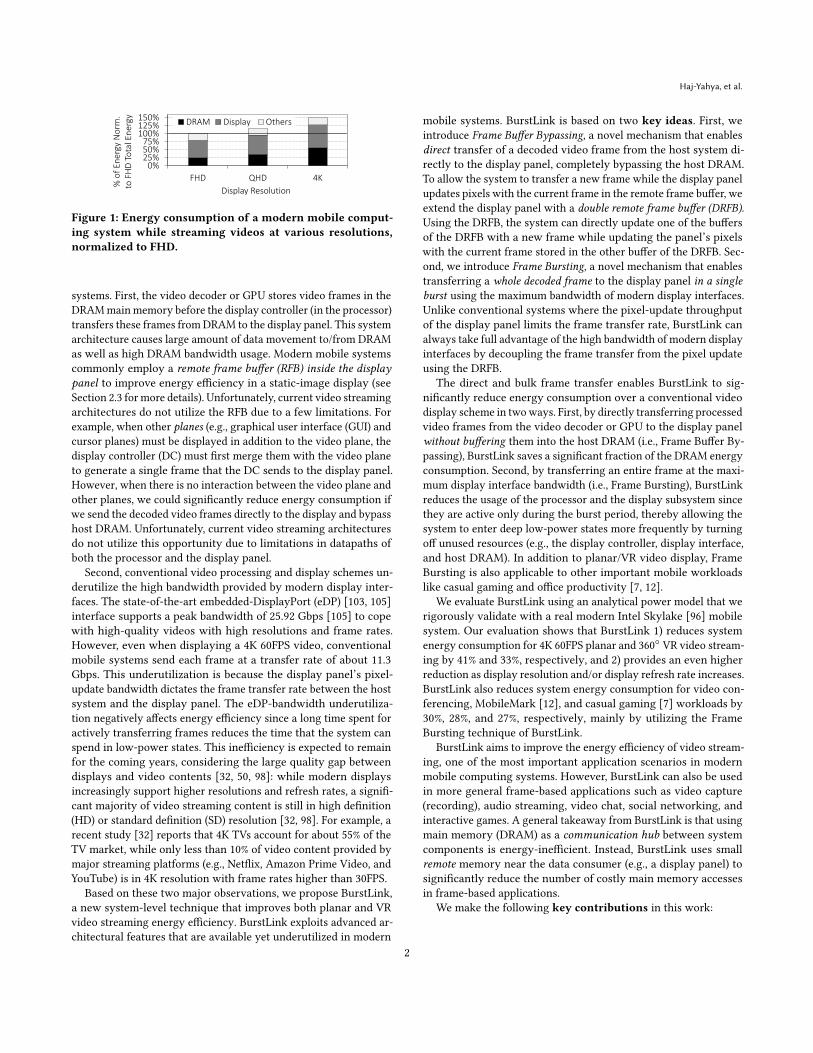
2 BACKGROUND2.1 Mobile SoC MicroarchitectureThe microarchitecture of a mobile system-on-chip (SoC) typicallyconsists of the following components.Main SoC Domains. A high-end mobile processor (e.g., Intel Sky-lake [27], AMD Kabini [16], Samsung Exynos [47]) is commonlyimplemented as an SoC that integrates three main domains into asingle chip: 1) compute domain, such as CPU cores and graphicsengines, 2) IO domain, which includes several intellectual proper-ties (IPs) sharing the IO interconnect (e.g., display controller (DC),image signal processing engine (ISP), video decoders (VDs), videoencoders (VEs)), and 3)memory domain, which includes thememorycontroller and the DRAM interface.IO Interconnect. IO interconnects, e.g., Intel On-chip System Fab-ric (IOSF) [65] and ARM Advanced Microcontroller Bus Architec-ture (AMBA) [10, 77], are on-chip communication technologies. IOInterconnect allows multiple IPs to 1) perform peer-to-peer (P2P)communication [76] and 2) access main memory (DRAM) usingdirect memory access (DMA) [67].P2P and DMA Engines. IO IPs are typically equipped with DMAand P2P engines [63]. The DMA engine enables the IP to accessthe main memory directly, while the P2P engine enables directcommunication between two IPs without copying data to mainmemory. P2P reduces the data transmission delay and increases theoverall available system bandwidth. DMA and P2P engines eachhave control registers (CRs) that the IP driver configures.Traditional Display Subsystem. Fig. 2 shows an overview of aconventional display subsystem, which consists of five main com-ponents: two on the processor side (i.e., the Video Decoder (VD) andDisplay Controller (DC)) and three on the display panel side (i.e.,the embedded-DisplayPort (eDP) Receiver, Pixel Formatter (PF), andRemote Frame Buffer (RFB), all inside the timing-controller (T-con)2).We explain video processing steps and power states in more detailin Sections 2.4 and 2.5, respectively, using Fig. 2 as a basis.
2A timing controller (T-con) is a circuit that processes and coordinates the col-oration of the pixels in a display panel [92].
Decoded Macroblocks
Memory Controller
Video Decoder (VD)
DisplayController (DC)
LCD Display
LCD Interface
eDPReceiver
Pixel Formatter (PF)
eDP
2 3
4
56
7
8
Processor Display Panel
Buffer
DRAM
…
CPU (application)
1
…
Remote Frame Buffer (RFB)
T-con
9…
Encoded Frames Frame Buffer
…
…
Network Chipset
…
a bEncoded Macroblocks
PMU
GPU
Interconnect
A
B
CD
Figure 2: Overview of a conventional display subsystem.
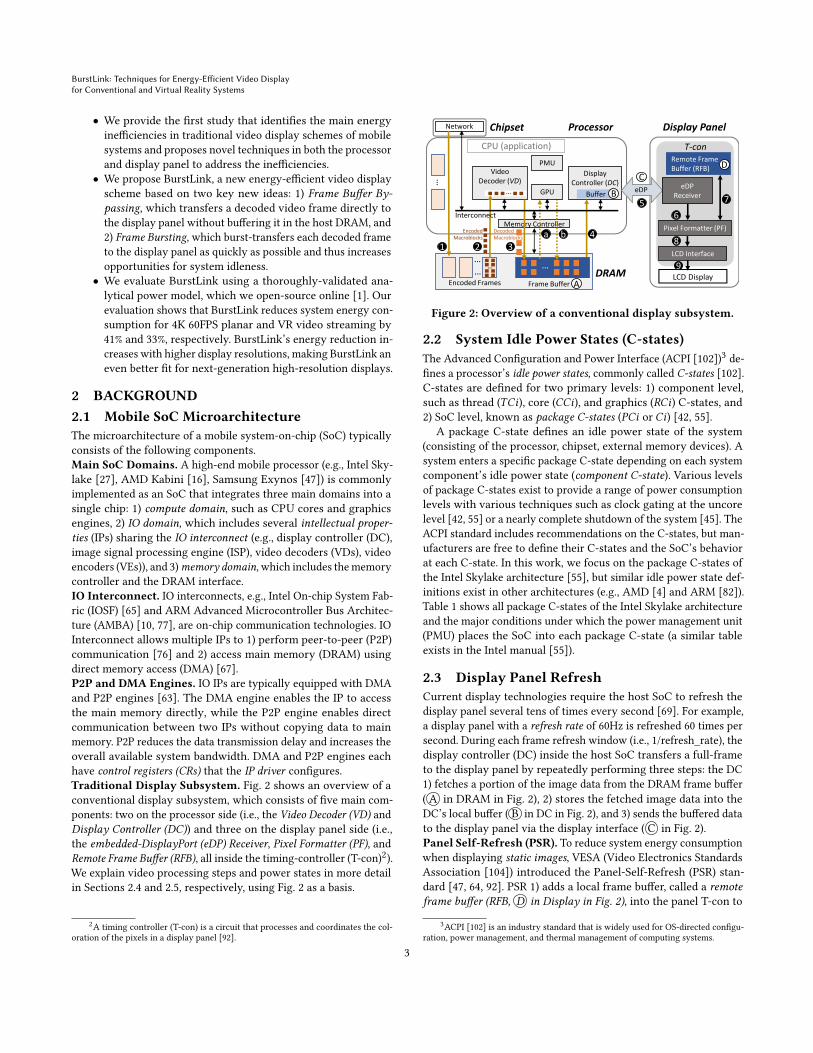
2.2 System Idle Power States (C-states)The Advanced Configuration and Power Interface (ACPI [102])3 de-fines a processor’s idle power states, commonly called C-states [102].C-states are defined for two primary levels: 1) component level,such as thread (𝑇𝐶𝑖), core (𝐶𝐶𝑖), and graphics (𝑅𝐶𝑖) C-states, and2) SoC level, known as package C-states (𝑃𝐶𝑖 or 𝐶𝑖) [42, 55].
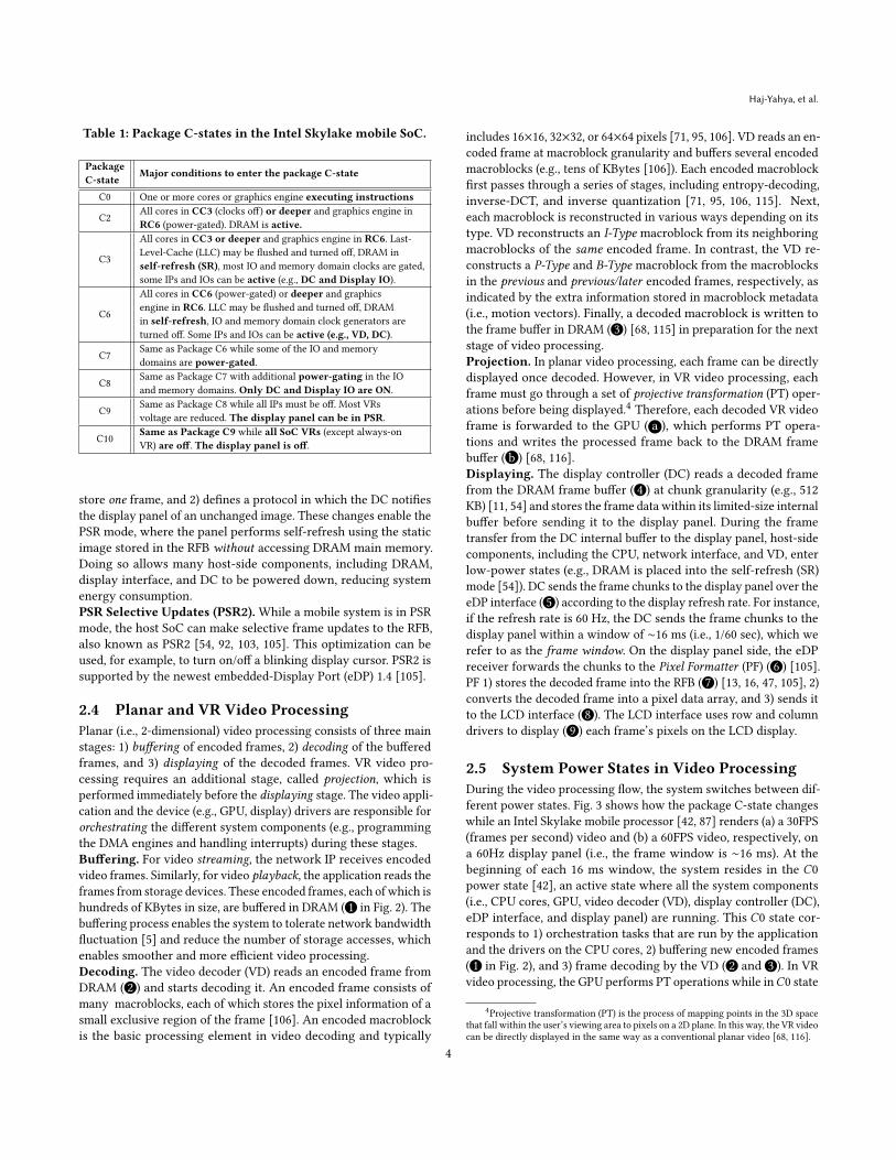
A package C-state defines an idle power state of the system(consisting of the processor, chipset, external memory devices). Asystem enters a specific package C-state depending on each systemcomponent’s idle power state (component C-state). Various levelsof package C-states exist to provide a range of power consumptionlevels with various techniques such as clock gating at the uncorelevel [42, 55] or a nearly complete shutdown of the system [45]. TheACPI standard includes recommendations on the C-states, but man-ufacturers are free to define their C-states and the SoC’s behaviorat each C-state. In this work, we focus on the package C-states ofthe Intel Skylake architecture [55], but similar idle power state def-initions exist in other architectures (e.g., AMD [4] and ARM [82]).Table 1 shows all package C-states of the Intel Skylake architectureand the major conditions under which the power management unit(PMU) places the SoC into each package C-state (a similar tableexists in the Intel manual [55]).
2.3 Display Panel RefreshCurrent display technologies require the host SoC to refresh thedisplay panel several tens of times every second [69]. For example,a display panel with a refresh rate of 60Hz is refreshed 60 times persecond. During each frame refresh window (i.e., 1/refresh_rate), thedisplay controller (DC) inside the host SoC transfers a full-frameto the display panel by repeatedly performing three steps: the DC1) fetches a portion of the image data from the DRAM frame buffer( A in DRAM in Fig. 2), 2) stores the fetched image data into theDC’s local buffer ( B in DC in Fig. 2), and 3) sends the buffered datato the display panel via the display interface ( C in Fig. 2).Panel Self-Refresh (PSR). To reduce system energy consumptionwhen displaying static images, VESA (Video Electronics StandardsAssociation [104]) introduced the Panel-Self-Refresh (PSR) stan-dard [47, 64, 92]. PSR 1) adds a local frame buffer, called a remoteframe buffer (RFB, D in Display in Fig. 2), into the panel T-con to
3ACPI [102] is an industry standard that is widely used for OS-directed configu-ration, power management, and thermal management of computing systems.
3
Haj-Yahya, et al.
Table 1: Package C-states in the Intel Skylake mobile SoC.
PackageC-state
Major conditions to enter the package C-state
C0 One or more cores or graphics engine executing instructions
C2 All cores in CC3 (clocks off) or deeper and graphics engine inRC6 (power-gated). DRAM is active.
C3
All cores in CC3 or deeper and graphics engine in RC6. Last-Level-Cache (LLC) may be flushed and turned off, DRAM inself-refresh (SR), most IO and memory domain clocks are gated,some IPs and IOs can be active (e.g., DC and Display IO).
C6
All cores in CC6 (power-gated) or deeper and graphicsengine in RC6. LLC may be flushed and turned off, DRAMin self-refresh, IO and memory domain clock generators areturned off. Some IPs and IOs can be active (e.g., VD, DC).
C7 Same as Package C6 while some of the IO and memorydomains are power-gated.
C8 Same as Package C7 with additional power-gating in the IOand memory domains. Only DC and Display IO are ON.
C9 Same as Package C8 while all IPs must be off. Most VRsvoltage are reduced. The display panel can be in PSR.
C10 Same as Package C9 while all SoC VRs (except always-onVR) are off. The display panel is off.
store one frame, and 2) defines a protocol in which the DC notifiesthe display panel of an unchanged image. These changes enable thePSR mode, where the panel performs self-refresh using the staticimage stored in the RFB without accessing DRAM main memory.Doing so allows many host-side components, including DRAM,display interface, and DC to be powered down, reducing systemenergy consumption.PSR Selective Updates (PSR2).While a mobile system is in PSRmode, the host SoC can make selective frame updates to the RFB,also known as PSR2 [54, 92, 103, 105]. This optimization can beused, for example, to turn on/off a blinking display cursor. PSR2 issupported by the newest embedded-Display Port (eDP) 1.4 [105].
2.4 Planar and VR Video ProcessingPlanar (i.e., 2-dimensional) video processing consists of three mainstages: 1) buffering of encoded frames, 2) decoding of the bufferedframes, and 3) displaying of the decoded frames. VR video pro-cessing requires an additional stage, called projection, which isperformed immediately before the displaying stage. The video appli-cation and the device (e.g., GPU, display) drivers are responsible fororchestrating the different system components (e.g., programmingthe DMA engines and handling interrupts) during these stages.Buffering. For video streaming, the network IP receives encodedvideo frames. Similarly, for video playback, the application reads theframes from storage devices. These encoded frames, each of which ishundreds of KBytes in size, are buffered in DRAM ( 1 in Fig. 2). Thebuffering process enables the system to tolerate network bandwidthfluctuation [5] and reduce the number of storage accesses, whichenables smoother and more efficient video processing.Decoding. The video decoder (VD) reads an encoded frame fromDRAM ( 2 ) and starts decoding it. An encoded frame consists ofmany macroblocks, each of which stores the pixel information of asmall exclusive region of the frame [106]. An encoded macroblockis the basic processing element in video decoding and typically
includes 16×16, 32×32, or 64×64 pixels [71, 95, 106]. VD reads an en-coded frame at macroblock granularity and buffers several encodedmacroblocks (e.g., tens of KBytes [106]). Each encoded macroblockfirst passes through a series of stages, including entropy-decoding,inverse-DCT, and inverse quantization [71, 95, 106, 115]. Next,each macroblock is reconstructed in various ways depending on itstype. VD reconstructs an I-Type macroblock from its neighboringmacroblocks of the same encoded frame. In contrast, the VD re-constructs a P-Type and B-Type macroblock from the macroblocksin the previous and previous/later encoded frames, respectively, asindicated by the extra information stored in macroblock metadata(i.e., motion vectors). Finally, a decoded macroblock is written tothe frame buffer in DRAM ( 3 ) [68, 115] in preparation for the nextstage of video processing.Projection. In planar video processing, each frame can be directlydisplayed once decoded. However, in VR video processing, eachframe must go through a set of projective transformation (PT) oper-ations before being displayed.4 Therefore, each decoded VR videoframe is forwarded to the GPU ( a ), which performs PT opera-tions and writes the processed frame back to the DRAM framebuffer ( b ) [68, 116].Displaying. The display controller (DC) reads a decoded framefrom the DRAM frame buffer ( 4 ) at chunk granularity (e.g., 512KB) [11, 54] and stores the frame data within its limited-size internalbuffer before sending it to the display panel. During the frametransfer from the DC internal buffer to the display panel, host-sidecomponents, including the CPU, network interface, and VD, enterlow-power states (e.g., DRAM is placed into the self-refresh (SR)mode [54]). DC sends the frame chunks to the display panel over theeDP interface ( 5 ) according to the display refresh rate. For instance,if the refresh rate is 60 Hz, the DC sends the frame chunks to thedisplay panel within a window of ∼16 ms (i.e., 1/60 sec), which werefer to as the frame window. On the display panel side, the eDPreceiver forwards the chunks to the Pixel Formatter (PF) ( 6 ) [105].PF 1) stores the decoded frame into the RFB ( 7 ) [13, 16, 47, 105], 2)converts the decoded frame into a pixel data array, and 3) sends itto the LCD interface ( 8 ). The LCD interface uses row and columndrivers to display ( 9 ) each frame’s pixels on the LCD display.
2.5 System Power States in Video ProcessingDuring the video processing flow, the system switches between dif-ferent power states. Fig. 3 shows how the package C-state changeswhile an Intel Skylake mobile processor [42, 87] renders (a) a 30FPS(frames per second) video and (b) a 60FPS video, respectively, ona 60Hz display panel (i.e., the frame window is ∼16 ms). At thebeginning of each 16 ms window, the system resides in the 𝐶0power state [42], an active state where all the system components(i.e., CPU cores, GPU, video decoder (VD), display controller (DC),eDP interface, and display panel) are running. This 𝐶0 state cor-responds to 1) orchestration tasks that are run by the applicationand the drivers on the CPU cores, 2) buffering new encoded frames( 1 in Fig. 2), and 3) frame decoding by the VD ( 2 and 3 ). In VRvideo processing, the GPU performs PT operations while in𝐶0 state
4Projective transformation (PT) is the process of mapping points in the 3D spacethat fall within the user’s viewing area to pixels on a 2D plane. In this way, the VR videocan be directly displayed in the same way as a conventional planar video [68, 116].
4
BurstLink: Techniques for Energy-Efficient Video Displayfor Conventional and Virtual Reality Systems
( a and b ). Once frame decoding state is complete, all the coresin the processor are powered off in the remaining frame window,while the DC 1) periodically fetches a chunk of the decoded framefrom DRAM to the DC buffer ( 4 ) and 2) continuously transfers thefetched data to the display panel ( 5 ). The system resides in the𝐶2 state while the DC fills its buffer. Once the DC buffer is full,the path to the host DRAM is closed, and the system enters the𝐶8 power state [42] where only the DC, eDP interface, and displaypanel are active. When the DC buffer is almost empty, the DC forcesthe system to return to the 𝐶2 state such that it can open the pathto the host DRAM and fetch the next chunk of the decoded frame.Note that the DC keeps transferring pixel data from its buffer to dis-play panel at a constant rate (which is determined by the display’spixel update rate) regardless of system power state transitions. Thispower state sequence repeats until the DC transfers a completedecoded frame to the display panel.
C0 C2 C8
frame window (~16ms)
…C2 C8 C2 C8 C0 C9 …
frame window (~16ms)
VD/GPUCPU DC fills its
buffer from
DRAM’s FB
DC sends pixels to the Panel
using DC’s buffer. DRAM is in SR.
CPU
Orchestration tasks. VD/GPU are off.
Panel enters PSR mode. The entire processor is off.
DRAM is in SR.A frame is ready in
DRAM’s FB
frame window (~16ms) frame window (~16ms)
C0 C2
(a)
(b)
C0 C2 C8 …C2 C8 C2 C8 C0 C2 C8 …C2 C8 C2 C8 …C0 C2
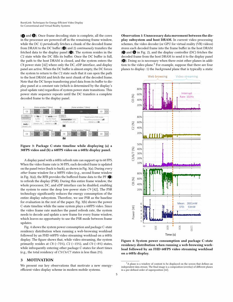
Figure 3: Package C-state timeline while displaying (a) a30FPS video and (b) a 60FPS video on a 60Hz display panel.
A display panel with a 60Hz refresh rate can support up to 60 FPS.When the video frame rate is 30 FPS, each decoded frame is updatedon the panel twice (back to back), as shown in Fig. 3(a). During everyother frame window for a 30FPS video (e.g., second frame windowin Fig. 3(a)), the RFB provides the buffered frame data to the PF ( 7 )to refresh the display (PSR). During this entire frame window, thewhole processor, DC, and eDP interface can be disabled, enablingthe system to enter the deep low-power state 𝐶9 [42]. The PSRtechnology significantly reduces the energy consumption of theentire display subsystem. Therefore, we use PSR as the baselinefor evaluation in the rest of the paper. Fig. 3(b) shows the powerC-state timeline while the same system plays a 60FPS video. Sincethe video frame rate matches the panel refresh rate, the systemneeds to decode and update a new frame for every frame window,which leaves no opportunity to use the PSR mode between frameupdates.
Fig. 4 shows the system power consumption and package C-stateresidency distribution when running a web-browsing workloadfollowed by an FHD 60FPS video streaming workload on a 60Hzdisplay. The figure shows that, while video streaming, the systemprimarily resides at 𝐶8 (∼75%), 𝐶2 (∼15%), and 𝐶0 (∼8%) states,while infrequently entering other package C-states for short times(e.g., the total residency of 𝐶3/𝐶6/𝐶7 states is less than 2%).
3 MOTIVATIONWe present our key observations that motivate a new energy-efficient video display scheme in modern mobile systems.
Observation 1: Unnecessary datamovement between the dis-play subsystem and host DRAM. In current video processingschemes, the video decoder (or GPU for virtual reality (VR) videos)stores each decoded frame into the frame buffer in the host DRAM( 3 and b in Fig. 2), and the display controller (DC) fetches thedecoded frame from the host DRAM to send it to the display panel( 4 ). Doing so is necessary when there exist other planes in addi-tion to the video plane.5 For example, suppose that there are fourplanes to display: 1) the background plane that is typically a static
20%
40%
60%
80%
10%
20%
30%
40%
50%
20%
40%
60%
80%
20%
40%
60%
80%
C0
(%
)C
2 (
%)
C3
/6/7
(%
)P
ow
er (
W)
Mean: 2831mW STD: 53mW
Interrupt Rate: 102Hz
654321
C8
(%
)
0 300
600
900
1200
Figure 4: System power consumption and package C-stateresidency distribution when running a web-browsing work-load followed by an FHD 60FPS video streaming workloadon a 60Hz display.
5A plane is a window of content to be displayed on the screen that defines anindependent data stream. The final image is a composition (overlay) of different planesin a pre-defined order of superposition [62].
5
Haj-Yahya, et al.
image, 2) the video plane that contains the video stream, 3) theapplication-graphic plane for the graphical user interface (GUI), and4) the cursor plane to display the cursor. In such a case, each planehas its frame buffer in the host DRAM. DC reads data chunks fromeach plane’s frame buffer, generates one composite chunk out ofthem, and sends the composite chunk to the display panel. However,when the user plays a video in full-screen mode (which is typical forplanar videos and is the default for VR videos), storing the decodedframe into the host DRAM first and then reading it again from thehost DRAM is unnecessary since there is no other plane for the DCto merge with the video plane. Bypassing the DRAM in such (com-mon) cases would significantly reduce unnecessary data movementover the power-hungry off-chip interconnects [26, 39, 72, 91] andthus improve energy efficiency. Our goal is to enable frame bufferbypassing whenever it is possible, with minimal changes to currentmobile SoC microarchitectures.Observation 2: Underutilization of the eDP interface ban-dwidth. As explained in Section 2.5, the system alternates betweenpower states C2 (when reading a chunk to the DC buffer) and C8(when the buffer is full) while the DC continuously sends a fulldecoded frame (e.g., 24 MB for a 4K resolution) to the display panel,which keeps both the DC and eDP receiver active during the en-tire frame window (e.g., ∼16 ms in a 60Hz refresh rate). However,the newest eDP interface [105] supports a maximum bandwidthof 25.92 Gbps, where it takes only 7.2 ms to transfer an entire 4Kdecoded frame. This means that the DC and eDP receiver can po-tentially switch to a power-saving mode for 55% of the 16ms framewindow after decoding and sending the entire frame in one burst.
The root cause for this inefficiency in conventional systems isthat the display controller, eDP receiver, and pixel-formatter (PF)are tightly coupled. For example, in a 4K display with a 60Hz refreshrate, the pixel update rate must be fixed to about 11.3 Gbps (i.e.,60 frames, each of which is 24 MB in size for 4K resolution, needsto be updated every second),which dictates the DC’s transfer ratethrough the eDP interface. The PF’s pixel update rate is determinedby the display panel’s resolution and refresh rate, in order to bealigned with the update rate of the LCD panel. Note that increasingthe PF’s pixel update rate without proper changes to the LCD panelwould cause image flickering and distortion [64].
Our goal is to eliminate the bottleneck in the display panel sothat the system directly transfers a full decoded frame from thevideo-decoder (or GPU) to the display panel in a burst, exploitingthe display interface’s maximum bandwidth. Doing so would (1)reduce the energy consumption of the host DRAM by eliminatingdata movement to/from the DRAM frame buffer, and (2) increasethe system’s idle-power state residency by reducing the usage ofthe processor and the display subsystem since they are active onlyduring the burst period.
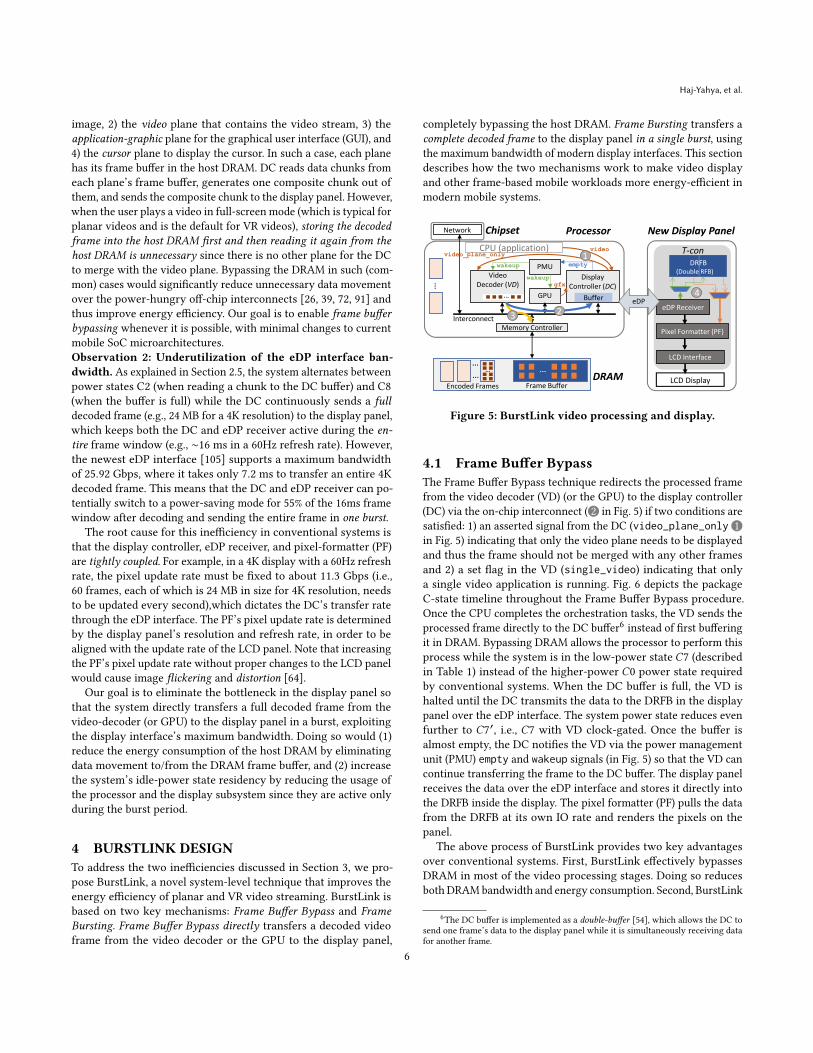
4 BURSTLINK DESIGNTo address the two inefficiencies discussed in Section 3, we pro-pose BurstLink, a novel system-level technique that improves theenergy efficiency of planar and VR video streaming. BurstLink isbased on two key mechanisms: Frame Buffer Bypass and FrameBursting. Frame Buffer Bypass directly transfers a decoded videoframe from the video decoder or the GPU to the display panel,
completely bypassing the host DRAM. Frame Bursting transfers acomplete decoded frame to the display panel in a single burst, usingthe maximum bandwidth of modern display interfaces. This sectiondescribes how the two mechanisms work to make video displayand other frame-based mobile workloads more energy-efficient inmodern mobile systems.
Memory Controller
Video Decoder (VD)
DisplayController (DC)
LCD Display
LCD Interface
Pixel Formatter (PF)
Processor New Display Panel
Buffer
DRAM
…
CPU (application)
…
T-con
…
Encoded Frames Frame Buffer
…
Network Chipset
…
emptyPMUwakeup
GPU
wakeup
Interconnect
…
3 2
video_plane_onlyvideo
1
gfx
eDP Receiver
DRFB(Double RFB)
eDP4
Figure 5: BurstLink video processing and display.
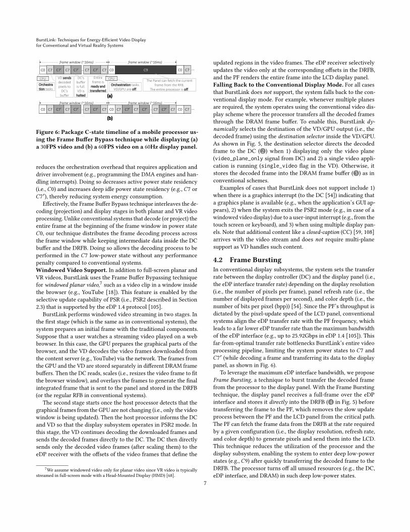
4.1 Frame Buffer BypassThe Frame Buffer Bypass technique redirects the processed framefrom the video decoder (VD) (or the GPU) to the display controller(DC) via the on-chip interconnect ( 2 in Fig. 5) if two conditions aresatisfied: 1) an asserted signal from the DC (video_plane_only 1in Fig. 5) indicating that only the video plane needs to be displayedand thus the frame should not be merged with any other framesand 2) a set flag in the VD (single_video) indicating that onlya single video application is running. Fig. 6 depicts the packageC-state timeline throughout the Frame Buffer Bypass procedure.Once the CPU completes the orchestration tasks, the VD sends theprocessed frame directly to the DC buffer6 instead of first bufferingit in DRAM. Bypassing DRAM allows the processor to perform thisprocess while the system is in the low-power state 𝐶7 (describedin Table 1) instead of the higher-power 𝐶0 power state requiredby conventional systems. When the DC buffer is full, the VD ishalted until the DC transmits the data to the DRFB in the displaypanel over the eDP interface. The system power state reduces evenfurther to 𝐶7′, i.e., 𝐶7 with VD clock-gated. Once the buffer isalmost empty, the DC notifies the VD via the power managementunit (PMU) empty and wakeup signals (in Fig. 5) so that the VD cancontinue transferring the frame to the DC buffer. The display panelreceives the data over the eDP interface and stores it directly intothe DRFB inside the display. The pixel formatter (PF) pulls the datafrom the DRFB at its own IO rate and renders the pixels on thepanel.
The above process of BurstLink provides two key advantagesover conventional systems. First, BurstLink effectively bypassesDRAM in most of the video processing stages. Doing so reducesboth DRAMbandwidth and energy consumption. Second, BurstLink
6The DC buffer is implemented as a double-buffer [54], which allows the DC tosend one frame’s data to the display panel while it is simultaneously receiving datafor another frame.
6
BurstLink: Techniques for Energy-Efficient Video Displayfor Conventional and Virtual Reality Systems
C7 C7’
frame window (~16ms)
…C7 C7’ C7 C7’ C0 C9 …
frame window (~16ms)
VD sendsdecoded pixels to
DC’s buffer
Orchestration tasks. VD/GPU are off.
The Panel can fetch the current frame from the RFB.
The entire processor is off.
C7C0
CPU
C7
Orchestration tasks
Entire frame is
ready and transferred
DC’s buffer is full. VD is
halted
C0
frame window (~16ms) frame window (~16ms)
(a)
(b)
C7 C7’ …C7 C7’ C7 C7’ C0 …C7C0 C7 C0C7 C7’ …C7 C7’ C7 C7’ C7
CPU
Figure 6: Package C-state timeline of a mobile processor us-ing the Frame Buffer Bypass technique while displaying (a)a 30FPS video and (b) a 60FPS video on a 60Hz display panel.
reduces the orchestration overhead that requires application anddriver involvement (e.g., programming the DMA engines and han-dling interrupts). Doing so decreases active power state residency(i.e., 𝐶0) and increases deep idle power state residency (e.g., 𝐶7 or𝐶7′), thereby reducing system energy consumption.
Effectively, the Frame Buffer Bypass technique interleaves the de-coding (projection) and display stages in both planar and VR videoprocessing. Unlike conventional systems that decode (or project) theentire frame at the beginning of the frame window in power state𝐶0, our technique distributes the frame decoding process acrossthe frame window while keeping intermediate data inside the DCbuffer and the DRFB. Doing so allows the decoding process to beperformed in the 𝐶7 low-power state without any performancepenalty compared to conventional systems.Windowed Video Support. In addition to full-screen planar andVR videos, BurstLink uses the Frame Buffer Bypassing techniquefor windowed planar video,7 such as a video clip in a window insidethe browser (e.g., YouTube [18]). This feature is enabled by theselective update capability of PSR (i.e., PSR2 described in Section2.3) that is supported by the eDP 1.4 protocol [105].
BurstLink performs windowed video streaming in two stages. Inthe first stage (which is the same as in conventional systems), thesystem prepares an initial frame with the traditional components.Suppose that a user watches a streaming video played on a webbrowser. In this case, the GPU prepares the graphical parts of thebrowser, and the VD decodes the video frames downloaded fromthe content server (e.g., YouTube) via the network. The frames fromthe GPU and the VD are stored separately in different DRAM framebuffers. Then the DC reads, scales (i.e., resizes the video frame to fitthe browser window), and overlays the frames to generate the finalintegrated frame that is sent to the panel and stored in the DRFB(or the regular RFB in conventional systems).
The second stage starts once the host processor detects that thegraphical frames from the GPU are not changing (i.e., only the videowindow is being updated). Then the host processor informs the DCand VD so that the display subsystem operates in PSR2 mode. Inthis stage, the VD continues decoding the downloaded frames andsends the decoded frames directly to the DC. The DC then directlysends only the decoded video frames (after scaling them) to theeDP receiver with the offsets of the video frames that define the
7We assume windowed video only for planar video since VR video is typicallystreamed in full-screen mode with a Head-Mounted Display (HMD) [68].
updated regions in the video frames. The eDP receiver selectivelyupdates the video only at the corresponding offsets in the DRFB,and the PF renders the entire frame into the LCD display panel.Falling Back to the Conventional Display Mode. For all casesthat BurstLink does not support, the system falls back to the con-ventional display mode. For example, whenever multiple planesare required, the system operates using the conventional video dis-play scheme where the processor transfers all the decoded framesthrough the DRAM frame buffer. To enable this, BurstLink dy-namically selects the destination of the VD/GPU output (i.e., thedecoded frame) using the destination selector inside the VD/GPU.As shown in Fig. 5, the destination selector directs the decodedframe to the DC ( 2 ) when 1) displaying only the video plane(video_plane_only signal from DC) and 2) a single video appli-cation is running (single_video flag in the VD). Otherwise, itstores the decoded frame into the DRAM frame buffer ( 3 ) as inconventional schemes.
Examples of cases that BurstLink does not support include 1)when there is a graphics interrupt (to the DC [54]) indicating thata graphics plane is available (e.g., when the application’s GUI ap-pears), 2) when the system exits the PSR2 mode (e.g., in case of awindowed video display) due to a user-input interrupt (e.g., from thetouch screen or keyboard), and 3) when using multiple display pan-els. Note that additional content like a closed-caption (CC) [59, 108]arrives with the video stream and does not require multi-planesupport as VD handles such content.
4.2 Frame BurstingIn conventional display subsystems, the system sets the transferrate between the display controller (DC) and the display panel (i.e.,the eDP interface transfer rate) depending on the display resolution(i.e., the number of pixels per frame), panel refresh rate (i.e., thenumber of displayed frames per second), and color depth (i.e., thenumber of bits per pixel (bpp)) [54]. Since the PF’s throughput isdictated by the pixel-update speed of the LCD panel, conventionalsystems align the eDP transfer rate with the PF frequency, whichleads to a far lower eDP transfer rate than the maximum bandwidthof the eDP interface (e.g., up to 25.92Gbps in eDP 1.4 [105]). Thisfar-from-optimal transfer rate bottlenecks BurstLink’s entire videoprocessing pipeline, limiting the system power states to 𝐶7 and𝐶7′ (while decoding a frame and transferring its data to the displaypanel, as shown in Fig. 6).
To leverage the maximum eDP interface bandwidth, we proposeFrame Bursting, a technique to burst transfer the decoded framefrom the processor to the display panel. With the Frame Burstingtechnique, the display panel receives a full-frame over the eDPinterface and stores it directly into the DRFB ( 4 in Fig. 5) beforetransferring the frame to the PF, which removes the slow updateprocess between the PF and the LCD panel from the critical path.The PF can fetch the frame data from the DRFB at the rate requiredby a given configuration (i.e., the display resolution, refresh rate,and color depth) to generate pixels and send them into the LCD.This technique reduces the utilization of the processor and thedisplay subsystem, enabling the system to enter deep low-powerstates (e.g., 𝐶9) after quickly transferring the decoded frame to theDRFB. The processor turns off all unused resources (e.g., the DC,eDP interface, and DRAM) in such deep low-power states.
7
Haj-Yahya, et al.
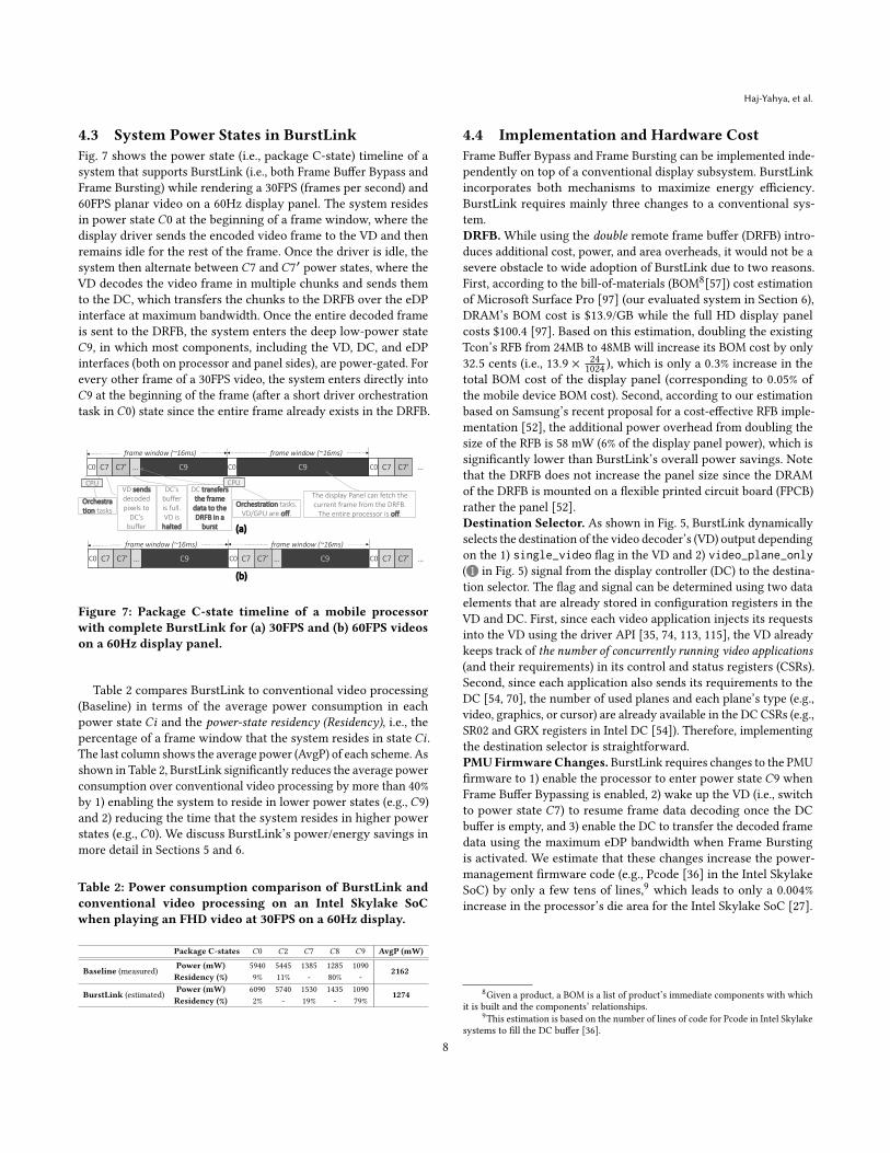
4.3 System Power States in BurstLinkFig. 7 shows the power state (i.e., package C-state) timeline of asystem that supports BurstLink (i.e., both Frame Buffer Bypass andFrame Bursting) while rendering a 30FPS (frames per second) and60FPS planar video on a 60Hz display panel. The system residesin power state 𝐶0 at the beginning of a frame window, where thedisplay driver sends the encoded video frame to the VD and thenremains idle for the rest of the frame. Once the driver is idle, thesystem then alternate between 𝐶7 and 𝐶7′ power states, where theVD decodes the video frame in multiple chunks and sends themto the DC, which transfers the chunks to the DRFB over the eDPinterface at maximum bandwidth. Once the entire decoded frameis sent to the DRFB, the system enters the deep low-power state𝐶9, in which most components, including the VD, DC, and eDPinterfaces (both on processor and panel sides), are power-gated. Forevery other frame of a 30FPS video, the system enters directly into𝐶9 at the beginning of the frame (after a short driver orchestrationtask in 𝐶0) state since the entire frame already exists in the DRFB.
frame window (~16ms) frame window (~16ms)
C9 …C0 C0
frame window (~16ms) frame window (~16ms)
C7 …C0 C0 C0C9
(a)
(b)
C7’ …
C7C0 C9C7’ …
C7C0 C9C7’ … C7 C7’
C7 C7’
VD sendsdecoded pixels to
DC’s buffer
Orchestration tasks. VD/GPU are off.
The display Panel can fetch the current frame from the DRFB.
The entire processor is off.
CPU
Orchestration tasks
DC transfers the frame data to the DRFB in a
burst
DC’s buffer is full. VD is
halted
CPU
Figure 7: Package C-state timeline of a mobile processorwith complete BurstLink for (a) 30FPS and (b) 60FPS videoson a 60Hz display panel.
Table 2 compares BurstLink to conventional video processing(Baseline) in terms of the average power consumption in eachpower state 𝐶𝑖 and the power-state residency (Residency), i.e., thepercentage of a frame window that the system resides in state 𝐶𝑖 .The last column shows the average power (AvgP) of each scheme. Asshown in Table 2, BurstLink significantly reduces the average powerconsumption over conventional video processing by more than 40%by 1) enabling the system to reside in lower power states (e.g., 𝐶9)and 2) reducing the time that the system resides in higher powerstates (e.g., 𝐶0). We discuss BurstLink’s power/energy savings inmore detail in Sections 5 and 6.
Table 2: Power consumption comparison of BurstLink andconventional video processing on an Intel Skylake SoCwhen playing an FHD video at 30FPS on a 60Hz display.
Package C-states 𝐶0 𝐶2 𝐶7 𝐶8 𝐶9 AvgP (mW)
Baseline (measured) Power (mW) 5940 5445 1385 1285 10902162
Residency (%) 9% 11% - 80% -
BurstLink (estimated) Power (mW) 6090 5740 1530 1435 10901274
Residency (%) 2% - 19% - 79%
4.4 Implementation and Hardware CostFrame Buffer Bypass and Frame Bursting can be implemented inde-pendently on top of a conventional display subsystem. BurstLinkincorporates both mechanisms to maximize energy efficiency.BurstLink requires mainly three changes to a conventional sys-tem.DRFB.While using the double remote frame buffer (DRFB) intro-duces additional cost, power, and area overheads, it would not be asevere obstacle to wide adoption of BurstLink due to two reasons.First, according to the bill-of-materials (BOM8[57]) cost estimationof Microsoft Surface Pro [97] (our evaluated system in Section 6),DRAM’s BOM cost is $13.9/GB while the full HD display panelcosts $100.4 [97]. Based on this estimation, doubling the existingTcon’s RFB from 24MB to 48MB will increase its BOM cost by only32.5 cents (i.e., 13.9 × 24
1024 ), which is only a 0.3% increase in thetotal BOM cost of the display panel (corresponding to 0.05% ofthe mobile device BOM cost). Second, according to our estimationbased on Samsung’s recent proposal for a cost-effective RFB imple-mentation [52], the additional power overhead from doubling thesize of the RFB is 58 mW (6% of the display panel power), which issignificantly lower than BurstLink’s overall power savings. Notethat the DRFB does not increase the panel size since the DRAMof the DRFB is mounted on a flexible printed circuit board (FPCB)rather the panel [52].Destination Selector. As shown in Fig. 5, BurstLink dynamicallyselects the destination of the video decoder’s (VD) output dependingon the 1) single_video flag in the VD and 2) video_plane_only( 1 in Fig. 5) signal from the display controller (DC) to the destina-tion selector. The flag and signal can be determined using two dataelements that are already stored in configuration registers in theVD and DC. First, since each video application injects its requestsinto the VD using the driver API [35, 74, 113, 115], the VD alreadykeeps track of the number of concurrently running video applications(and their requirements) in its control and status registers (CSRs).Second, since each application also sends its requirements to theDC [54, 70], the number of used planes and each plane’s type (e.g.,video, graphics, or cursor) are already available in the DC CSRs (e.g.,SR02 and GRX registers in Intel DC [54]). Therefore, implementingthe destination selector is straightforward.PMUFirmware Changes. BurstLink requires changes to the PMUfirmware to 1) enable the processor to enter power state 𝐶9 whenFrame Buffer Bypassing is enabled, 2) wake up the VD (i.e., switchto power state 𝐶7) to resume frame data decoding once the DCbuffer is empty, and 3) enable the DC to transfer the decoded framedata using the maximum eDP bandwidth when Frame Burstingis activated. We estimate that these changes increase the power-management firmware code (e.g., Pcode [36] in the Intel SkylakeSoC) by only a few tens of lines,9 which leads to only a 0.004%increase in the processor’s die area for the Intel Skylake SoC [27].
8Given a product, a BOM is a list of product’s immediate components with whichit is built and the components’ relationships.
9This estimation is based on the number of lines of code for Pcode in Intel Skylakesystems to fill the DC buffer [36].
8
BurstLink: Techniques for Energy-Efficient Video Displayfor Conventional and Virtual Reality Systems
4.5 Generalization of BurstLink TechniquesBurstLink aims to improve the energy efficiency of video streaming(which is one of the most important application scenarios in modernmobile systems). However, the proposed techniques can also be usedin more general frame-based applications such as video capture(recording), audio streaming, video chat, social networking, andinteractive games. A general takeaway from BurstLink is that usingmain memory (DRAM) as a communication hub between systemcomponents is energy-inefficient. Instead, BurstLink uses smallremote memory (e.g., 48MB DRFB, which is only 0.3% of 16GBDRAM) near the data consumer (e.g., a display panel) or the dataproducer (e.g., a camera sensor) to significantly reduce the numberof costly main memory accesses in frame-based applications.
5 EXPERIMENTAL METHODOLOGYWe outline our methodology for evaluating BurstLink. First, wedescribe our workloads. Second, we introduce our new industry-grade analytical powermodel for evaluating the baseline system andBurstLink. We open-source our model online [1]. Third, we discussour process for validating our model against power measurementsfrom a real modern mobile device that is based on the Intel Skylakesystem.
5.1 WorkloadsWe evaluate BurstLink with planar and VR video-streaming work-loads [7, 24], which are used in standard industrial benchmarksfor battery-life [2, 7, 78–80] and academic evaluations of video-streaming optimizations [15, 28, 33, 68, 73, 74, 85, 113, 115, 116].These workloads typically assume that only a single application(e.g., video streaming in our evaluation) runs on the system. Insmartphones and tablets, the currently used application typicallyruns in full-screen mode, while the other opened applications arenormally sent to the background and moved to a suspended state.This assumption is also true of our evaluated system, the MicrosoftSurface [109] when running in Tablet-Mode [99].
5.2 Analytical Power ModelModeling the Baseline System. We develop a new analyticalpower model that estimates the average system power, 𝑃𝑜𝑤𝑒𝑟𝑎𝑣𝑔 ,within a frame window, as follows:
𝑃𝑜𝑤𝑒𝑟𝑎𝑣𝑔 =∑10𝑖=0 𝑃𝐶𝑖
· 𝑅𝐶𝑖+ 𝑃_𝑒𝑛𝐶𝑖
· 𝐿𝑎𝑡_𝑒𝑛𝐶𝑖+ 𝑃_𝑒𝑥𝐶𝑖
· 𝐿𝑎𝑡_𝑒𝑥𝐶𝑖
𝑃𝐶𝑖denotes the average system power consumption in power state
𝐶𝑖 (e.g., package C-states in Table 1). 𝑃_𝑒𝑛𝐶𝑖and 𝑃_𝑒𝑥𝐶𝑖
denotethe average power consumption while entering and exiting state𝐶𝑖 , respectively. 𝑅𝐶𝑖
denotes the residency at power state 𝐶𝑖 , i.e.,the percentage of the total time the system spends at power state𝐶𝑖 . 𝐿𝑎𝑡_𝑒𝑛𝐶𝑖
(𝐿𝑎𝑡_𝑒𝑥𝐶𝑖) denotes the latency for entering (exiting)
power state 𝐶𝑖 . We use a synthetic benchmark to 1) place the sys-tem in different power states, and 2) measure entry and exit la-tencies [90]. We obtain power state residency using processor’sresidency reporting counters [55]. Our power model inherentlyaccounts for major system parameters such as 1) DC buffer size,2) DRAM capacity, 3) DRAM bandwidth, and 4) eDP bandwidth.These parameters can directly affect each state’s residency and
power consumption, and the frequency with which the systemswitches between power states.
For power states in which the DRAM is active (i.e., not in self-refresh, such as in package𝐶0 and𝐶2 states as shown in Table 1), thepower state’s average system power consumption (i.e., 𝑃𝐶𝑖
) dependsalso on DRAM power, which is correlated to DRAM bandwidth. Wemodel DRAMpower consumption in two parts: 1) background power,which is consumed regardless of memory access characteristics andonly depends on DRAM power states (i.e., self-refresh, CKE-High(active), CKE-Low (fast power-down) [26]), and 2) operating power,which highly depends on DRAM read/write bandwidth [19, 26, 34].First, to model background power, we record the time spent in eachDRAM power state. We weight the power consumption in eachstate by the measured time values to obtain the average backgroundpower. Note that the DRAM power states in our processor arecorrelated to the package C-states. For example, DRAM is in theactive (CKE-High) state only in 𝐶0 and 𝐶2 states while it is inthe self-refresh state in all other package C-states. Second, wemodel the operating power by multiplying the average power perunit read/write bandwidth (e.g., 1 GB/s) by the actual read/writebandwidth consumed. To determine the average power per unit read(write) bandwidth, we 1) run a memory benchmark that generatesreads (writes) at different bandwidth values (similar to [94]), 2)measure DRAM power consumption, and 3) extrapolate the powerconsumption per 1GB/s reads (writes).Modeling the BurstLink System.Wemodel the power consump-tion of the system enhanced with the two techniques of BurstLinkusing measured data from our baseline power model. The two tech-niques of BurstLink affect both the residency and power level ateach package C-state. For example, 𝐶9 residency increases as thesystem finishes transferring each decoded frame more quickly.
We carefully model the estimated average power consumption(i.e., 𝑃𝐶𝑖
) and the residency (i.e., 𝑅𝐶𝑖) at each power state 𝐶𝑖 with
BurstLink, taking into account two essential factors. 1) Inactive sys-tem components (e.g., power-gated DC or DRAM in the self-refreshstate) in each power state. 2) Changes in each SoC component’soperating frequency (e.g., the DC and eDP interface consume morepower when using the maximum eDP bandwidth for Frame Burst-ing). We plug in the new values in our analytical model to estimatethe average system power consumption when applying each ofBurstLink’s techniques.
5.3 Measurements and Power Model ValidationBaseline System. We use an Intel reference design for high-endtablet devices [114], such as the Microsoft Surface Pro [109]. Ourbaseline system is equipped with an Intel Skylake [27, 31] processor(whose specifications are summarized in Table 3), and multipledebug/configuration capabilities.
Table 3: Baseline system.
Processor Intel i5-6300U Skylake [96], 14 nm, TDP: 15 WFrequencies: 800-2400 MHz, L3: 3 MB
Memory LPDDR3-1866MHz [56], 8 GB, dual-channel
To validate our power model for the baseline and BurstLink sys-tems, we carry out the following steps: 1) we measure the average
9
Haj-Yahya, et al.
power and residency at each power state in the baseline system,2) we break down the measured power into system components,and 3) we measure the effect of frequency/bandwidth changes onthe average power and residency at each power-state. We compareall our power measurements to the estimations provided by ourpower model.Measurement Setup. For the system power measurements, weuse a Keysight N6705B DC power analyzer [60] equipped withan N6781A source measurement unit (SMU) [61]. The N6705B isnormally used for high-accuracy (around 99.975% [61]) power mea-surement of low-power devices (e.g., smartphones and tablets).The power analyzer measures and logs the instantaneous powerconsumption of different device components. Control/analysis soft-ware (14585A [60]) for data visualization and management runs ona separate laptop connected to the power analyzer.
Fig. 8 shows the power measurement setup of the Intel Skylakemobile system [27, 31, 44, 112] under study. The system has abattery and multiple power supplies (i.e., voltage regulators [40,41]) for the mobile system components. We refer the reader to theKeysight manual [60] for more detail on the actual connectionsof measurement wires to the N6705B power analyzer, the designunder test (DUT), DUT’s battery, and control/analysis software.The power analyzer can measure the power consumption of thedifferent power states (𝐶0, 𝐶2, and 𝐶7–9) in a single experiment.We measure the residency of each C-state using the Intel VTuneprofiler [53] on our evaluated workloads.
VD DC
DRAMCPUChipset Memory ControllerDMI
Battery
V_Core V_GFX V_SA V_DV_IOV_C
Display
VDDQ
Graphics(GFX)
acdefgh
…
N6705B Power Analyzer
Processor
Network
DDRIO
eDP
VDD
T
b
DUT (Tablet) N6705B
Voltage Regulators
Processor & Chipset
DRAM
eDPWiFi eMMC
Figure 8: Power measurement of the Intel Skylake mobilesystem using the Keysight N6705B DC power analyzer [60](left). Illustration of Microsoft Surface Pro tablet’s systemcomponents [109] (right).
Baseline Power Measurements. We carry out multiple measure-ments for different system components, including the processor,DRAM, chipset, and display. As illustrated in Fig. 8, we connectthe power analyzer’s four channels to measurement points a-f forindividual power domains, and measurement point T for the totalsystem power drained out of the battery. For the processor power,we measure four voltage domains: 1) V_Core, the voltage supplyfor cores and last-level-cache (LLC), 2) V_GFX, the voltage supplyfor the graphics engine and the VD, 3) V_IO, the voltage supplyfor the IOs including the eDP DRAM, DDRIO (digital part), andthe interface to the chipset, and 4) V_SA, the voltage supply forthe system agent10 that contains several controllers, including thememory controller and DC. Each measurement uses four analogchannels with a 50-`s sampling interval.
10SA stands for System Agent which houses the traditional Northbridge chip[23, 83]. SA contains several functionalities, such as the memory controller and the IOcontrollers/engines [39, 40, 45, 107].
Power Breakdown into SystemComponents.We further breakdown the measured processor power consumption into proces-sor’s sub-components (e.g., VD, DC, eDP, memory-controller) usingpower estimation techniques [38]. Using the design characteristicsof these components (such as capacitance, leakage, operational fre-quency, and voltage), we estimate their relative power consumption.Next, using the measured power consumption of the system, we es-timate the power of each component. Note that other power estima-tion techniques can also be used to determine this component-levelpower breakdown [14, 17, 66].Power Model Accuracy. To validate our model, we run four rep-resentative battery life workloads [7]: web browsing, light gaming,video conferencing, and video playback with multiple display res-olution setups. We measure average system power (as explainedabove) and collect package C-states residencies along with eachrun. We use our analytical power model to estimate the averagepower consumption of these workloads. Then, we compare themeasured vs. estimated average power consumption. We find thatthe accuracy of our analytical power model is approximately 96%for the evaluated workloads. The accuracy for each of the fourmainly-used power states in our battery-life workloads, 𝐶0, 𝐶2, 𝐶7,and 𝐶8, is 97.4%, 96.2%, 95.1%, and 94.7%, respectively.
6 EVALUATIONWe evaluate BurstLink against the baseline video display system(described in Fig. 2) with five studies. 1) We study energy reductionfor four different display resolutions for planar video streaming. 2)We show energy reduction of different workloads and resolutionsfor VR video streaming. 3) We show the effect of frame rate onBurstLink energy reduction. 4) We compare BurstLink to state-of-the-art techniques that reduce the energy consumption of videoprocessing. 5)We evaluate the benefits of BurstLink for othermobileworkloads than video display.
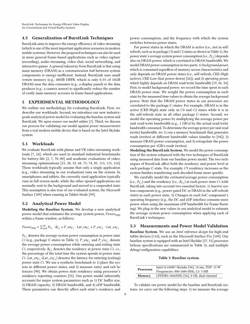
6.1 Planar Video Streaming Energy ReductionFig. 9 shows the energy consumption of each technique of BurstLink(i.e., Frame Bursting and Frame Buffer Bypassing) and the fullBurstLink, normalized to the baseline system, averaged across framewindows of 30 FPS videos displaying on a 60 Hz panel.
00.20.40.60.8
1
FHD QHD 4K 5KEner
gy N
orm
. to
Bas
elin
e
Display Resolution
Baseline Burst Bypass BurstLink
Figure 9: Total system energy reduction of Frame Bursting,Frame Buffer Bypassing, and BurstLink for 30 FPSHD video.
We make two major observations. First, BurstLink reduces theoverall system energy consumption by 37% for an 𝐹𝐻𝐷 display.Frame Bursting and Frame Buffer Bypassing reduce overall energyby 23% and 31% compared to the baseline, respectively. Second,BurstLink’s energy reduction increases as display resolution in-creases. For a 5𝐾 display, BurstLink reduces the overall systemenergy by ∼42%.
10
BurstLink: Techniques for Energy-Efficient Video Displayfor Conventional and Virtual Reality Systems
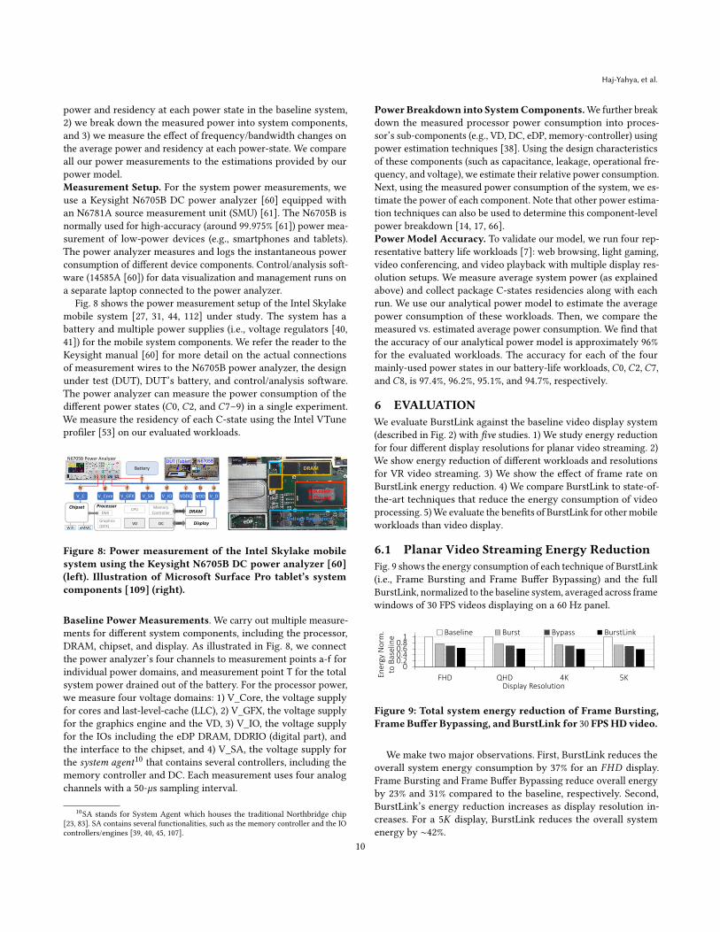
Fig. 10 compares BurstLink’s system energy consumption break-down across three major system components, i.e., DRAM, display,and others (which includes the processor, WiFi network card, andeMMC storage) with that of the baseline system. BurstLink reducesthe total dissipated energy of DRAM by 3.8× and 5.7× for 𝐹𝐻𝐷and 5𝐾 resolutions, respectively. The higher the video resolution,the higher the DRAM’s relative energy consumption out of theentire system energy consumption, and therefore, the higher theenergy reduction of BurstLink. BurstLink reduces the total dissi-pated energy of others by 13.1× and 2.1× for 𝐹𝐻𝐷 and 5𝐾 resolu-tions, respectively. The higher the video resolution, the lower theprocessor’s relative energy consumption out of the entire systemenergy consumption, and therefore, the lower the energy reductionof BurstLink.
00.20.40.60.8
1
Baseline BurstLink Baseline BurstLink Baseline BurstLink Baseline BurstLink
FHD QHD 4K 5K
Ener
gy N
orm
. to
Bas
elin
e
Display Resolution
DRAM Display Others
Figure 10: Energy breakdown into system components.
6.2 VR Video Streaming Energy ReductionFig. 11 shows the energy reduction of five 360◦ VR streaming work-loads [24] when running with BurstLink. We assume an optimizedstate-of-the-art VR streaming scheme [68, 116] in the baseline,which significantly reduces the compute energy compared to tradi-tional schemes.
0%
10%
20%
30%
40%
Elephant Paris Rollercoaster Timelapse Rhino
Ener
gy R
ed. (
%)
0%10%20%30%40%
960 x1080
1080 x1200
1280 x1440
1440 x1600
Ener
gy R
ed. (
%)
(a) (b)
Figure 11: (a) VR video streaming energy reduction for fiveVRworkloads. (b) Energy reduction for different VR displayresolutions of theRhinoworkload (otherworkloads are sim-ilar).
We make two major observations. First, BurstLink reduces theoverall system energy consumption by up to 33%. Compute-energy-dominant (mainly GPU) workloads have lower benefits compared tomemory-energy-dominant workloads (as would be expected), sinceBurstLink greatly reduces memory energy. Second, BurstLink’sbenefits decrease as VR display resolution increases. This is mainlybecause compute energy becomes more dominant in VR workloadsas display resolution increases [68, 116], which leaves less relativepotential for BurstLink to save in memory energy.
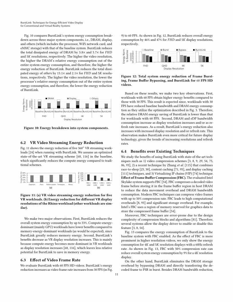
6.3 Effect of Video Frame RateWe evaluate BurstLink with 60 FPS HD videos. BurstLink’s energyreduction increases as video frame rate increases from 30 FPS (in Fig.
9) to 60 FPS. As shown in Fig. 12, BurstLink reduces overall energyconsumption by 46% and 47% for 𝐹𝐻𝐷 and 5𝐾 display resolutions,respectively.
00.20.40.60.8
1
FHD QHD 4K 5K
Ener
gy N
orm
. to
Bas
elin
e
Display Resolution
Baseline Burst Bypass BurstLink
Figure 12: Total system energy reduction of Frame Burst-ing, Frame Buffer Bypassing, and BurstLink for 60 FPS HDvideos.
Based on these results, we make two key observations. First,workloads with 60 FPS obtain higher energy benefits compared tothose with 30 FPS. This result is expected since, workloads with 30FPS have reduced baseline bandwidth and DRAM energy consump-tion as they utilize the optimization described in Fig. 3. Therefore,the relative DRAM energy saving of BurstLink is lower than thatfor workloads with 60 FPS. Second, DRAM and eDP bandwidthconsumption increase as display resolution increases and/or as re-fresh rate increases. As a result, BurstLink’s energy reduction alsoincreases with increased display resolution and/or refresh rate. Thisobservation makes BurstLink even more critical for future displaytechnology, given the trends of increasing resolutions and refreshrates.
6.4 Benefits over Existing TechniquesWe study the benefits of using BurstLink with state-of-the-art tech-niques such as 1) video compression schemes [3, 8, 9, 29, 54, 75,86, 93], 2) a recent technique by Zhang et al. [115] that combinesrace-to-sleep [25, 30], content caching [71, 95], and display caching[111] techniques, and 3) Virtualizing IP chains (VIP) [74] technique.Effect of FrameBuffer Compression (FBC). The evaluated IntelSkylake system supports FBC [54]. FBC compresses a decoded videoframe before storing it in the frame buffer region in host DRAMto reduce the data movement overhead and DRAM bandwidthconsumption. Modern FBC techniques can compress video frameswith up to 50% compression rate. FBC leads to high computationaloverheads [8, 93] and significant storage overhead. For example,Intel’s FBC uses a region of memory reserved for graphics data tostore the compressed frame buffer [54].
Moreover, FBC techniques are error-prone due to the designcomplexity of compression blocks and algorithms [81]. Therefore,several systems allow the display driver to enable or disable thisfeature [3, 8, 54].
Fig. 13 compares the energy consumption of BurstLink to thebaseline system with FBC enabled. As the effect of FBC is moreprominent in higher resolution videos, we only show the energyconsumption for 4𝐾 and 5𝐾 resolution displays with a 60Hz refreshrate. As shown in Fig. 13, FBC with 50% compression rate canreduce overall system energy consumption by 9% for a 4𝐾 resolutiondisplay.
On the other hand, BurstLink eliminates the DRAM storageoverhead by bypassing DRAM and directly transferring the de-coded frame to PSR in burst. Besides DRAM bandwidth reduction,
11
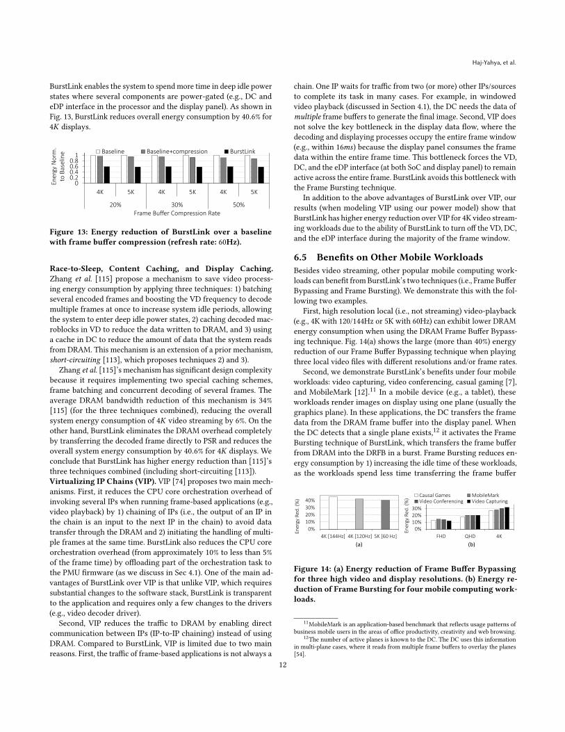
Haj-Yahya, et al.
BurstLink enables the system to spend more time in deep idle powerstates where several components are power-gated (e.g., DC andeDP interface in the processor and the display panel). As shown inFig. 13, BurstLink reduces overall energy consumption by 40.6% for4𝐾 displays.
00.20.40.60.8
1
4K 5K 4K 5K 4K 5K
20% 30% 50%
Ener
gy N
orm
. to
Bas
elin
e
Frame Buffer Compression Rate
Baseline Baseline+compression BurstLink
Figure 13: Energy reduction of BurstLink over a baselinewith frame buffer compression (refresh rate: 60Hz).
Race-to-Sleep, Content Caching, and Display Caching.Zhang et al. [115] propose a mechanism to save video process-ing energy consumption by applying three techniques: 1) batchingseveral encoded frames and boosting the VD frequency to decodemultiple frames at once to increase system idle periods, allowingthe system to enter deep idle power states, 2) caching decoded mac-roblocks in VD to reduce the data written to DRAM, and 3) usinga cache in DC to reduce the amount of data that the system readsfrom DRAM. This mechanism is an extension of a prior mechanism,short-circuiting [113], which proposes techniques 2) and 3).
Zhang et al. [115]’s mechanism has significant design complexitybecause it requires implementing two special caching schemes,frame batching and concurrent decoding of several frames. Theaverage DRAM bandwidth reduction of this mechanism is 34%[115] (for the three techniques combined), reducing the overallsystem energy consumption of 4𝐾 video streaming by 6%. On theother hand, BurstLink eliminates the DRAM overhead completelyby transferring the decoded frame directly to PSR and reduces theoverall system energy consumption by 40.6% for 4𝐾 displays. Weconclude that BurstLink has higher energy reduction than [115]’sthree techniques combined (including short-circuiting [113]).Virtualizing IP Chains (VIP). VIP [74] proposes two main mech-anisms. First, it reduces the CPU core orchestration overhead ofinvoking several IPs when running frame-based applications (e.g.,video playback) by 1) chaining of IPs (i.e., the output of an IP inthe chain is an input to the next IP in the chain) to avoid datatransfer through the DRAM and 2) initiating the handling of multi-ple frames at the same time. BurstLink also reduces the CPU coreorchestration overhead (from approximately 10% to less than 5%of the frame time) by offloading part of the orchestration task tothe PMU firmware (as we discuss in Sec 4.1). One of the main ad-vantages of BurstLink over VIP is that unlike VIP, which requiressubstantial changes to the software stack, BurstLink is transparentto the application and requires only a few changes to the drivers(e.g., video decoder driver).
Second, VIP reduces the traffic to DRAM by enabling directcommunication between IPs (IP-to-IP chaining) instead of usingDRAM. Compared to BurstLink, VIP is limited due to two mainreasons. First, the traffic of frame-based applications is not always a
chain. One IP waits for traffic from two (or more) other IPs/sourcesto complete its task in many cases. For example, in windowedvideo playback (discussed in Section 4.1), the DC needs the data ofmultiple frame buffers to generate the final image. Second, VIP doesnot solve the key bottleneck in the display data flow, where thedecoding and displaying processes occupy the entire frame window(e.g., within 16𝑚𝑠) because the display panel consumes the framedata within the entire frame time. This bottleneck forces the VD,DC, and the eDP interface (at both SoC and display panel) to remainactive across the entire frame. BurstLink avoids this bottleneck withthe Frame Bursting technique.
In addition to the above advantages of BurstLink over VIP, ourresults (when modeling VIP using our power model) show thatBurstLink has higher energy reduction over VIP for 4K video stream-ing workloads due to the ability of BurstLink to turn off the VD, DC,and the eDP interface during the majority of the frame window.
6.5 Benefits on Other Mobile WorkloadsBesides video streaming, other popular mobile computing work-loads can benefit fromBurstLink’s two techniques (i.e., Frame BufferBypassing and Frame Bursting). We demonstrate this with the fol-lowing two examples.
First, high resolution local (i.e., not streaming) video-playback(e.g., 4K with 120/144Hz or 5K with 60Hz) can exhibit lower DRAMenergy consumption when using the DRAM Frame Buffer Bypass-ing technique. Fig. 14(a) shows the large (more than 40%) energyreduction of our Frame Buffer Bypassing technique when playingthree local video files with different resolutions and/or frame rates.
Second, we demonstrate BurstLink’s benefits under four mobileworkloads: video capturing, video conferencing, casual gaming [7],and MobileMark [12].11 In a mobile device (e.g., a tablet), theseworkloads render images on display using one plane (usually thegraphics plane). In these applications, the DC transfers the framedata from the DRAM frame buffer into the display panel. Whenthe DC detects that a single plane exists,12 it activates the FrameBursting technique of BurstLink, which transfers the frame bufferfrom DRAM into the DRFB in a burst. Frame Bursting reduces en-ergy consumption by 1) increasing the idle time of these workloads,as the workloads spend less time transferring the frame buffer
(a) (b)
0%10%20%30%40%
FHD QHD 4K
Ener
gy R
ed. (
%)
Causal Games MobileMarkVideo Conferencing Video Capturing
0%
10%
20%
30%
40%
4K [144Hz] 4K [120Hz] 5K [60 Hz]
Ener
gy R
ed. (
%)
Figure 14: (a) Energy reduction of Frame Buffer Bypassingfor three high video and display resolutions. (b) Energy re-duction of Frame Bursting for four mobile computing work-loads.
11MobileMark is an application-based benchmark that reflects usage patterns ofbusiness mobile users in the areas of office productivity, creativity and web browsing.
12The number of active planes is known to the DC. The DC uses this informationin multi-plane cases, where it reads from multiple frame buffers to overlay the planes[54].
12
BurstLink: Techniques for Energy-Efficient Video Displayfor Conventional and Virtual Reality Systems
and more time in low-power states, and 2) power-gating the DCand the eDP interface at both the processor and the display panel.Fig. 14(b) shows the large energy reduction of Frame Bursting forfour workloads on a high-end tablet.
7 RELATEDWORKTo our knowledge, this is the first work to leverage Panel-Self-Refresh memory to improve the energy efficiency of video process-ing in modern mobile computing systems. BurstLink significantlyreduces costly data movement between DRAM and display subsys-tem components and enables frame transfer with the maximumdisplay bandwidth, which allows the system to reside in lowerpower states. We briefly discuss related prior work that we classifyinto five categories.Buffer Compression. Many prior works [8, 9, 29, 51, 86, 93, 110]propose various frame buffer compression techniques, such as run-length encoding (RLE) [93] and differential pulse code modulation(DPCM) [93], which increase the effective DRAM bandwidth (byreducing the amount of transferred frame data) and thus improvedisplay processing performance. We already show that BurstLinkoutperforms frame buffer compression (Section 6.4).Batching of Decoded Frames. Zhang et al. [115] propose threeoptimizations to increase the idle time (race to halt) and reducebandwidth from VD to DRAM and DRAM to DC in video process-ing. Their proposals lie across batch processing, content and displaycaching and frequency/voltage optimization. We already demon-strate the clear advantages of BurstLink over these optimizations(Section 6.4).
Other prior works [20, 58, 101] propose different batching andpipelining techniques at a macro-block level. As BurstLink offers toachieve energy efficiency through leveraging PSR memory directly,similar techniques for batch processing can be easily combinedwith our proposal to increase energy improvement.Optimizing Frequency/Voltage. Several prior works improve en-ergy efficiency by reducing the voltage and frequency of 1) thelogic used for decoding/encoding [73, 84, 85] or 2) multiple systemdomains [39]. BurstLink, on the other hand, does not depend onfrequency/voltage scaling for its energy improvement.Other PSR-based proposals. Prior works [13, 16, 46, 47, 64, 92,103] use the PSR frame buffer mainly for static images rather thanbypassing DRAM. BurstLink uses the PSR for static and dynamic im-ages to skip costly data movement and significantly reduce DRAMenergy consumption.
8 CONCLUSIONWe introduce BurstLink, a new energy-efficient planar and VR videodisplay scheme that uses display panel local memory to eliminatebuffering frames in main memory. BurstLink directly transfers a fulldecoded frame from the video-decoder (or GPU) to the display panelin a burst, exploiting the display interface’s maximum bandwidth.Doing so (1) reduces the energy consumption of the host DRAM byeliminating data movement to/from the DRAM frame buffer, and(2) increases the system’s idle-power state residency by reducingthe usage of the processor and the display subsystem since theyare active only during the burst period. BurstLink reduces systemenergy consumption for 4K planar and VR video streaming by 41%
and 33%, respectively, and its benefits increase as display resolutionand/or refresh rate increases. As video consumption in mobiledevices continues to increase sharply, along with an increase indisplay resolution to meet user satisfaction, BurstLink is poisedto provide high energy efficiency in current and next-generationmobile processors. BurstLink’s techniques can also be used in moregeneral frame-based applications such as video capture (recording),audio streaming, video chat, social networking, and interactivegames.
A general takeaway from BurstLink is that using main memory(DRAM) as a communication hub between system components isenergy-inefficient. Instead, BurstLink uses small remote memorynear the data consumer (e.g., a display panel) to significantly re-duce the number of costly main memory accesses in frame-basedapplications.
ACKNOWLEDGMENTSWe thank the anonymous reviewers of ASPLOS 2021, ISCA 2021,and MICRO 2021 for feedback. We thank the SAFARI ResearchGroup members for valuable feedback and the stimulating intel-lectual environment they provide. We acknowledge the generousgifts provided by our industrial partners: Google, Huawei, Intel,Microsoft, and VMware. An earlier version of this paper was placedon arxiv.org on 11 April 2021 [43].
REFERENCES[1] BurstLink Source Code. https://github.com/CMU-SAFARI/BurstLink. 2021.[2] 9to5mac. iPhone 11 and iPhone 11 Pro Improves on iPhone XR Stellar Battery
Life. https://bit.ly/34Rlx5A. 2020.[3] AMD. RADEON: Dissecting the Polaris Architecture. AMD Whitepaper. 2016.[4] AMD. AMD Processor Specifications. https://bit.ly/3zQV46u. 2020.[5] Pablo Ameigeiras, Juan J Ramos-Munoz, Jorge Navarro-Ortiz, and Juan M Lopez-
Soler. Analysis and Modeling of YouTube Traffic. ETT. 2012.[6] Anandtech. Lenovo Launches Legion Y740S Ultra-Thin 4K 15.6-Inch Gaming
Notebook. https://bit.ly/39kxz7J. 2020.[7] Anandtech. The Microsoft Surface Pro (2017) Review: Evaluation.
https://bit.ly/2WCB3yZ. 2020.[8] ARM. ARM Frame Buffer Compression. https://bit.ly/2WsvG5X. 2016.[9] ARM. Transaction Elimination. https://bit.ly/2qI3rmy. 2016.[10] ARM. AMBA: The Standard for On-Chip Communication. https://bit.ly/2UEzQ8l.
2020.[11] ARM. ARM Mali Display Processors. https://bit.ly/33b01Yk. 2021.[12] BAPCo. MobileMark 2014. https://bapco.com/products/mobilemark-2018. 2019.[13] Omri Barkay, WLAN Engineer, IT Dave Buchholz, IT Dan Codorean, IT Doug
DeVetter, and Baz Stevens. Evaluating Intel® ProWireless Display for EnterpriseUse. Intel White Paper. 2013.
[14] Ramon Bertran, Marc Gonzalez, Xavier Martorell, Nacho Navarro, and EduardAyguade. A SystematicMethodology to Generate Decomposable and ResponsivePower Models for CMPs. TC. 2013.
[15] Amirali Boroumand, Saugata Ghose, Youngsok Kim, Rachata Ausavarungnirun,Eric Shiu, Rahul Thakur, et al. Google Workloads for Consumer Devices: Miti-gating Data Movement Bottlenecks. In ASPLOS. 2018.
[16] Dan Bouvier, Brad Cohen, Walter Fry, Sreekanth Godey, and Michael Mantor.AMD Kabini APU SoC. In Hot Chips. 2013.
[17] David Brooks, Pradip Bose, Viji Srinivasan, Michael K Gschwind, Philip G Emma,and Michael G Rosenfield. NewMethodology for Early-stage, Microarchitecture-level Power-Performance Analysis of Microprocessors. IBM J. Res. Dev. 2003.
[18] Jean Burgess and Joshua Green. YouTube: Online Video and Participatory Culture.John Wiley & Sons. 2018.
[19] Kevin K Chang, Abdullah Giray Yaglıkçı, Saugata Ghose, Aditya Agrawal, Niladr-ish Chatterjee, Abhijith Kashyap, et al. Voltron: Understanding and Exploitingthe Voltage-Latency-Reliability Trade-Offs in Modern DRAM Chips to ImproveEnergy Efficiency. SIGMETRICS. 2017.
[20] Tung-Chien Chen, Yu-Wen Huang, and Liang-Gee Chen. Analysis and Designof Macroblock Pipelining for H.264/AVC VLSI Architecture. In ISCAS. 2004.
[21] Inseok Choi, Hojun Shim, and Naehyuck Chang. Low-power Color TFT LCDDisplay for Hand-held Embedded Systems. In ISLPED. 2002.
13
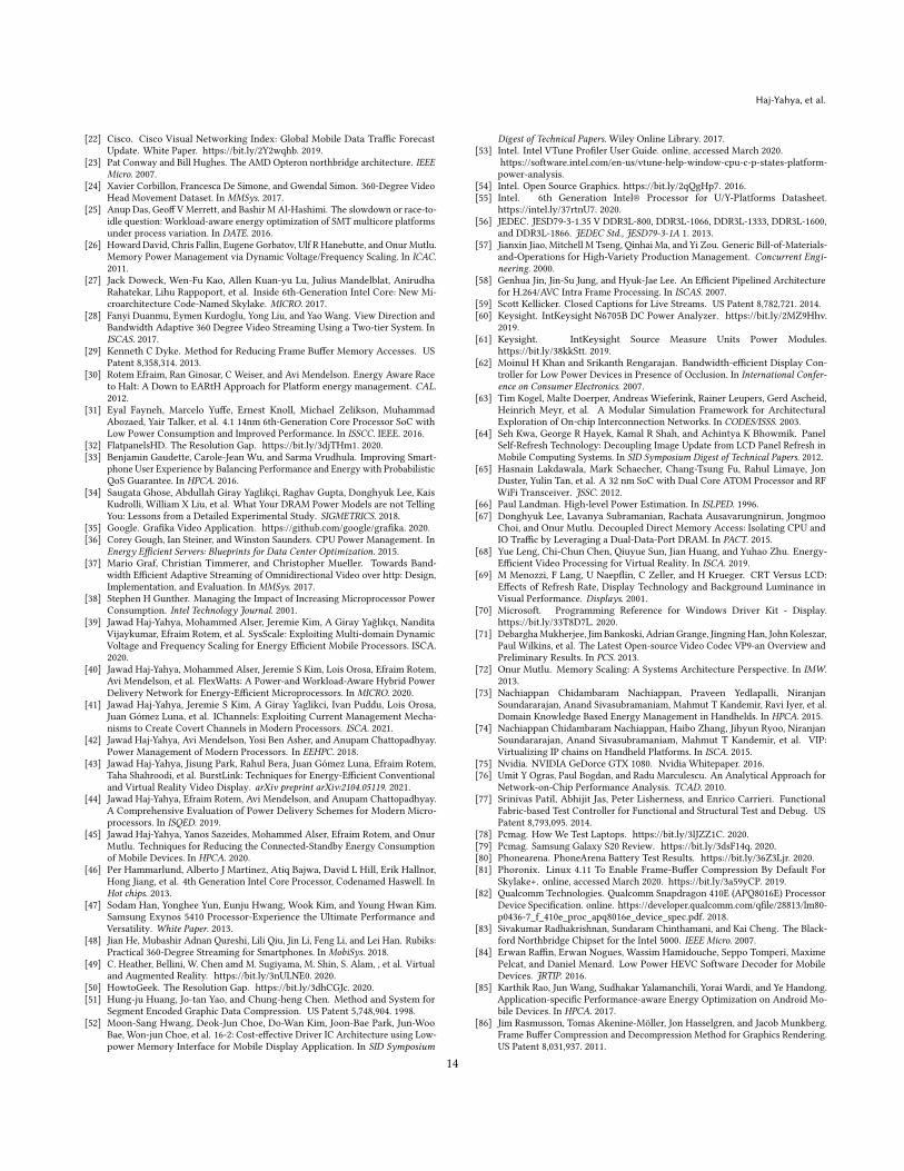
Haj-Yahya, et al.
[22] Cisco. Cisco Visual Networking Index: Global Mobile Data Traffic ForecastUpdate. White Paper. https://bit.ly/2Y2wqhb. 2019.
[23] Pat Conway and Bill Hughes. The AMD Opteron northbridge architecture. IEEEMicro. 2007.
[24] Xavier Corbillon, Francesca De Simone, and Gwendal Simon. 360-Degree VideoHead Movement Dataset. In MMSys. 2017.
[25] Anup Das, Geoff VMerrett, and Bashir M Al-Hashimi. The slowdown or race-to-idle question: Workload-aware energy optimization of SMT multicore platformsunder process variation. In DATE. 2016.
[26] Howard David, Chris Fallin, Eugene Gorbatov, Ulf R Hanebutte, and Onur Mutlu.Memory Power Management via Dynamic Voltage/Frequency Scaling. In ICAC.2011.
[27] Jack Doweck, Wen-Fu Kao, Allen Kuan-yu Lu, Julius Mandelblat, AnirudhaRahatekar, Lihu Rappoport, et al. Inside 6th-Generation Intel Core: New Mi-croarchitecture Code-Named Skylake. MICRO. 2017.
[28] Fanyi Duanmu, Eymen Kurdoglu, Yong Liu, and Yao Wang. View Direction andBandwidth Adaptive 360 Degree Video Streaming Using a Two-tier System. InISCAS. 2017.
[29] Kenneth C Dyke. Method for Reducing Frame Buffer Memory Accesses. USPatent 8,358,314. 2013.
[30] Rotem Efraim, Ran Ginosar, C Weiser, and Avi Mendelson. Energy Aware Raceto Halt: A Down to EARtH Approach for Platform energy management. CAL.2012.
[31] Eyal Fayneh, Marcelo Yuffe, Ernest Knoll, Michael Zelikson, MuhammadAbozaed, Yair Talker, et al. 4.1 14nm 6th-Generation Core Processor SoC withLow Power Consumption and Improved Performance. In ISSCC. IEEE. 2016.
[32] FlatpanelsHD. The Resolution Gap. https://bit.ly/3djTHm1. 2020.[33] Benjamin Gaudette, Carole-Jean Wu, and Sarma Vrudhula. Improving Smart-
phone User Experience by Balancing Performance and Energy with ProbabilisticQoS Guarantee. In HPCA. 2016.
[34] Saugata Ghose, Abdullah Giray Yaglikçi, Raghav Gupta, Donghyuk Lee, KaisKudrolli, William X Liu, et al. What Your DRAM Power Models are not TellingYou: Lessons from a Detailed Experimental Study. SIGMETRICS. 2018.
[35] Google. Grafika Video Application. https://github.com/google/grafika. 2020.[36] Corey Gough, Ian Steiner, and Winston Saunders. CPU Power Management. In
Energy Efficient Servers: Blueprints for Data Center Optimization. 2015.[37] Mario Graf, Christian Timmerer, and Christopher Mueller. Towards Band-
width Efficient Adaptive Streaming of Omnidirectional Video over http: Design,Implementation, and Evaluation. In MMSys. 2017.
[38] Stephen H Gunther. Managing the Impact of Increasing Microprocessor PowerConsumption. Intel Technology Journal. 2001.
[39] Jawad Haj-Yahya, Mohammed Alser, Jeremie Kim, A Giray Yağlıkçı, NanditaVijaykumar, Efraim Rotem, et al. SysScale: Exploiting Multi-domain DynamicVoltage and Frequency Scaling for Energy Efficient Mobile Processors. ISCA.2020.
[40] Jawad Haj-Yahya, Mohammed Alser, Jeremie S Kim, Lois Orosa, Efraim Rotem,Avi Mendelson, et al. FlexWatts: A Power-and Workload-Aware Hybrid PowerDelivery Network for Energy-Efficient Microprocessors. In MICRO. 2020.
[41] Jawad Haj-Yahya, Jeremie S Kim, A Giray Yaglikci, Ivan Puddu, Lois Orosa,Juan Gómez Luna, et al. IChannels: Exploiting Current Management Mecha-nisms to Create Covert Channels in Modern Processors. ISCA. 2021.
[42] Jawad Haj-Yahya, Avi Mendelson, Yosi Ben Asher, and Anupam Chattopadhyay.Power Management of Modern Processors. In EEHPC. 2018.
[43] Jawad Haj-Yahya, Jisung Park, Rahul Bera, Juan Gómez Luna, Efraim Rotem,Taha Shahroodi, et al. BurstLink: Techniques for Energy-Efficient Conventionaland Virtual Reality Video Display. arXiv preprint arXiv:2104.05119. 2021.
[44] Jawad Haj-Yahya, Efraim Rotem, Avi Mendelson, and Anupam Chattopadhyay.A Comprehensive Evaluation of Power Delivery Schemes for Modern Micro-processors. In ISQED. 2019.
[45] Jawad Haj-Yahya, Yanos Sazeides, Mohammed Alser, Efraim Rotem, and OnurMutlu. Techniques for Reducing the Connected-Standby Energy Consumptionof Mobile Devices. In HPCA. 2020.
[46] Per Hammarlund, Alberto J Martinez, Atiq Bajwa, David L Hill, Erik Hallnor,Hong Jiang, et al. 4th Generation Intel Core Processor, Codenamed Haswell. InHot chips. 2013.
[47] Sodam Han, Yonghee Yun, Eunju Hwang, Wook Kim, and Young Hwan Kim.Samsung Exynos 5410 Processor-Experience the Ultimate Performance andVersatility. White Paper. 2013.
[48] Jian He, Mubashir Adnan Qureshi, Lili Qiu, Jin Li, Feng Li, and Lei Han. Rubiks:Practical 360-Degree Streaming for Smartphones. In MobiSys. 2018.
[49] C. Heather, Bellini, W. Chen amd M. Sugiyama, M. Shin, S. Alam, , et al. Virtualand Augmented Reality. https://bit.ly/3nULNE0. 2020.
[50] HowtoGeek. The Resolution Gap. https://bit.ly/3dhCGJc. 2020.[51] Hung-ju Huang, Jo-tan Yao, and Chung-heng Chen. Method and System for
Segment Encoded Graphic Data Compression. US Patent 5,748,904. 1998.[52] Moon-Sang Hwang, Deok-Jun Choe, Do-Wan Kim, Joon-Bae Park, Jun-Woo
Bae, Won-jun Choe, et al. 16-2: Cost-effective Driver IC Architecture using Low-power Memory Interface for Mobile Display Application. In SID Symposium
Digest of Technical Papers. Wiley Online Library. 2017.[53] Intel. Intel VTune Profiler User Guide. online, accessed March 2020.
https://software.intel.com/en-us/vtune-help-window-cpu-c-p-states-platform-power-analysis.
[54] Intel. Open Source Graphics. https://bit.ly/2qQgHp7. 2016.[55] Intel. 6th Generation Intel® Processor for U/Y-Platforms Datasheet.
https://intel.ly/37rtnU7. 2020.[56] JEDEC. JESD79-3-1.35 V DDR3L-800, DDR3L-1066, DDR3L-1333, DDR3L-1600,
and DDR3L-1866. JEDEC Std., JESD79-3-1A 1. 2013.[57] Jianxin Jiao, Mitchell M Tseng, Qinhai Ma, and Yi Zou. Generic Bill-of-Materials-
and-Operations for High-Variety Production Management. Concurrent Engi-neering. 2000.
[58] Genhua Jin, Jin-Su Jung, and Hyuk-Jae Lee. An Efficient Pipelined Architecturefor H.264/AVC Intra Frame Processing. In ISCAS. 2007.
[59] Scott Kellicker. Closed Captions for Live Streams. US Patent 8,782,721. 2014.[60] Keysight. IntKeysight N6705B DC Power Analyzer. https://bit.ly/2MZ9Hhv.
2019.[61] Keysight. IntKeysight Source Measure Units Power Modules.
https://bit.ly/38kkStt. 2019.[62] Moinul H Khan and Srikanth Rengarajan. Bandwidth-efficient Display Con-
troller for Low Power Devices in Presence of Occlusion. In International Confer-ence on Consumer Electronics. 2007.
[63] Tim Kogel, Malte Doerper, Andreas Wieferink, Rainer Leupers, Gerd Ascheid,Heinrich Meyr, et al. A Modular Simulation Framework for ArchitecturalExploration of On-chip Interconnection Networks. In CODES/ISSS. 2003.
[64] Seh Kwa, George R Hayek, Kamal R Shah, and Achintya K Bhowmik. PanelSelf-Refresh Technology: Decoupling Image Update from LCD Panel Refresh inMobile Computing Systems. In SID Symposium Digest of Technical Papers. 2012.
[65] Hasnain Lakdawala, Mark Schaecher, Chang-Tsung Fu, Rahul Limaye, JonDuster, Yulin Tan, et al. A 32 nm SoC with Dual Core ATOM Processor and RFWiFi Transceiver. JSSC. 2012.
[66] Paul Landman. High-level Power Estimation. In ISLPED. 1996.[67] Donghyuk Lee, Lavanya Subramanian, Rachata Ausavarungnirun, Jongmoo
Choi, and Onur Mutlu. Decoupled Direct Memory Access: Isolating CPU andIO Traffic by Leveraging a Dual-Data-Port DRAM. In PACT. 2015.
[68] Yue Leng, Chi-Chun Chen, Qiuyue Sun, Jian Huang, and Yuhao Zhu. Energy-Efficient Video Processing for Virtual Reality. In ISCA. 2019.
[69] M Menozzi, F Lang, U Naepflin, C Zeller, and H Krueger. CRT Versus LCD:Effects of Refresh Rate, Display Technology and Background Luminance inVisual Performance. Displays. 2001.
[70] Microsoft. Programming Reference for Windows Driver Kit - Display.https://bit.ly/33T8D7L. 2020.
[71] DebarghaMukherjee, Jim Bankoski, AdrianGrange, JingningHan, JohnKoleszar,Paul Wilkins, et al. The Latest Open-source Video Codec VP9-an Overview andPreliminary Results. In PCS. 2013.
[72] Onur Mutlu. Memory Scaling: A Systems Architecture Perspective. In IMW.2013.
[73] Nachiappan Chidambaram Nachiappan, Praveen Yedlapalli, NiranjanSoundararajan, Anand Sivasubramaniam, Mahmut T Kandemir, Ravi Iyer, et al.Domain Knowledge Based Energy Management in Handhelds. In HPCA. 2015.
[74] Nachiappan Chidambaram Nachiappan, Haibo Zhang, Jihyun Ryoo, NiranjanSoundararajan, Anand Sivasubramaniam, Mahmut T Kandemir, et al. VIP:Virtualizing IP chains on Handheld Platforms. In ISCA. 2015.
[75] Nvidia. NVIDIA GeDorce GTX 1080. Nvidia Whitepaper. 2016.[76] Umit Y Ogras, Paul Bogdan, and Radu Marculescu. An Analytical Approach for
Network-on-Chip Performance Analysis. TCAD. 2010.[77] Srinivas Patil, Abhijit Jas, Peter Lisherness, and Enrico Carrieri. Functional
Fabric-based Test Controller for Functional and Structural Test and Debug. USPatent 8,793,095. 2014.
[78] Pcmag. How We Test Laptops. https://bit.ly/3lJZZ1C. 2020.[79] Pcmag. Samsung Galaxy S20 Review. https://bit.ly/3dsF14q. 2020.[80] Phonearena. PhoneArena Battery Test Results. https://bit.ly/36Z3Ljr. 2020.[81] Phoronix. Linux 4.11 To Enable Frame-Buffer Compression By Default For
Skylake+. online, accessed March 2020. https://bit.ly/3a59yCP. 2019.[82] Qualcomm Technologies. Qualcomm Snapdragon 410E (APQ8016E) Processor
Device Specification. online. https://developer.qualcomm.com/qfile/28813/lm80-p0436-7_f_410e_proc_apq8016e_device_spec.pdf. 2018.
[83] Sivakumar Radhakrishnan, Sundaram Chinthamani, and Kai Cheng. The Black-ford Northbridge Chipset for the Intel 5000. IEEE Micro. 2007.
[84] Erwan Raffin, Erwan Nogues, Wassim Hamidouche, Seppo Tomperi, MaximePelcat, and Daniel Menard. Low Power HEVC Software Decoder for MobileDevices. JRTIP. 2016.
[85] Karthik Rao, Jun Wang, Sudhakar Yalamanchili, Yorai Wardi, and Ye Handong.Application-specific Performance-aware Energy Optimization on Android Mo-bile Devices. In HPCA. 2017.
[86] Jim Rasmusson, Tomas Akenine-Möller, Jon Hasselgren, and Jacob Munkberg.Frame Buffer Compression and Decompression Method for Graphics Rendering.US Patent 8,031,937. 2011.
14
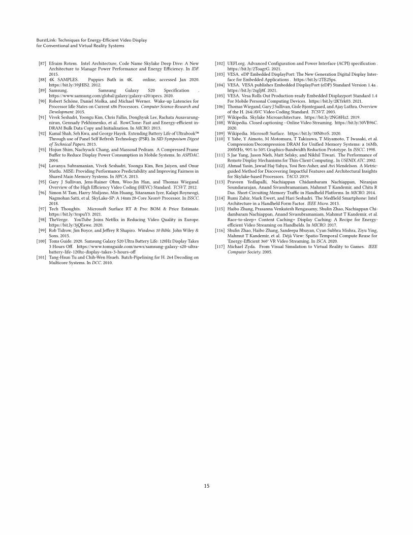
BurstLink: Techniques for Energy-Efficient Video Displayfor Conventional and Virtual Reality Systems
[87] Efraim Rotem. Intel Architecture, Code Name Skylake Deep Dive: A NewArchitecture to Manage Power Performance and Energy Efficiency. In IDF.2015.
[88] 4K SAMPLES. Puppies Bath in 4K. online, accessed Jan 2020.https://bit.ly/39jHIS2. 2012.
[89] Samsung. Samsung Galaxy S20 Specification .https://www.samsung.com/global/galaxy/galaxy-s20/specs. 2020.
[90] Robert Schöne, Daniel Molka, and Michael Werner. Wake-up Latencies forProcessor Idle States on Current x86 Processors. Computer Science-Research andDevelopment. 2015.
[91] Vivek Seshadri, Yoongu Kim, Chris Fallin, Donghyuk Lee, Rachata Ausavarung-nirun, Gennady Pekhimenko, et al. RowClone: Fast and Energy-efficient in-DRAM Bulk Data Copy and Initialization. In MICRO. 2013.
[92] Kamal Shah, Seh Kwa, and George Hayek. Extending Battery Life of Ultrabook™Through use of Panel Self Refresh Technology (PSR). In SID Symposium Digestof Technical Papers. 2013.
[93] Hojun Shim, Nachyuck Chang, and Massoud Pedram. A Compressed FrameBuffer to Reduce Display Power Consumption in Mobile Systems. In ASPDAC.2004.
[94] Lavanya Subramanian, Vivek Seshadri, Yoongu Kim, Ben Jaiyen, and OnurMutlu. MISE: Providing Performance Predictability and Improving Fairness inShared Main Memory Systems. In HPCA. 2013.
[95] Gary J Sullivan, Jens-Rainer Ohm, Woo-Jin Han, and Thomas Wiegand.Overview of the High Efficiency Video Coding (HEVC) Standard. TCSVT. 2012.
[96] Simon M Tam, Harry Muljono, Min Huang, Sitaraman Iyer, Kalapi Royneogi,Nagmohan Satti, et al. SkyLake-SP: A 14nm 28-Core Xeon® Processor. In ISSCC.2018.
[97] Tech Thoughts. Microsoft Surface RT & Pro: BOM & Price Estimate.https://bit.ly/3rspuY3. 2021.
[98] TheVerge. YouTube Joins Netflix in Reducing Video Quality in Europe.https://bit.ly/3jQEewe. 2020.
[99] Rob Tidrow, Jim Boyce, and Jeffrey R Shapiro. Windows 10 Bible. John Wiley &Sons. 2015.
[100] Toms Guide. 2020. Samsung Galaxy S20 Ultra Battery Life: 120Hz Display Takes3 Hours Off. https://www.tomsguide.com/news/samsung-galaxy-s20-ultra-battery-life-120hz-display-takes-3-hours-off
[101] Tang-Hsun Tu and Chih-Wen Hsueh. Batch-Pipelining for H. 264 Decoding onMulticore Systems. In DCC. 2010.
[102] UEFI.org. Advanced Configuration and Power Interface (ACPI) specification .https://bit.ly/2ToagrG. 2021.
[103] VESA. eDP Embedded DisplayPort: The New Generation Digital Display Inter-face for Embedded Applications . https://bit.ly/2TE2Sps.
[104] VESA. VESA publishes Embedded DisplayPort (eDP) Standard Version 1.4a .https://bit.ly/2sglj8f. 2021.
[105] VESA. Vesa Rolls Out Production-ready Embedded Displayport Standard 1.4For Mobile Personal Computing Devices. https://bit.ly/2KYrk03. 2021.
[106] ThomasWiegand, Gary J Sullivan, Gisle Bjontegaard, andAjay Luthra. Overviewof the H. 264/AVC Video Coding Standard. TCSVT. 2003.
[107] Wikipedia. Skylake Microarchitecture. https://bit.ly/2NG8Hz2. 2019.[108] Wikipedia. Closed captioning - Online Video Streaming. https://bit.ly/30VB96C.
2020.[109] Wikipedia. Microsoft Surface. https://bit.ly/38N8vrS. 2020.[110] Y Yabe, Y Aimoto, M Motomura, T Takizawa, T Miyamoto, T Iwasaki, et al.
Compression/Decompression DRAM for Unified Memory Systems: a 16Mb,200MHz, 90% to 50% Graphics-Bandwidth Reduction Prototype. In ISSCC. 1998.
[111] S Jae Yang, Jason Nieh, Matt Selsky, and Nikhil Tiwari. The Performance ofRemote Display Mechanisms for Thin-Client Computing.. In USENIX ATC. 2002.
[112] Ahmad Yasin, Jawad Haj-Yahya, Yosi Ben-Asher, and Avi Mendelson. A Metric-guided Method for Discovering Impactful Features and Architectural Insightsfor Skylake-based Processors. TACO. 2019.
[113] Praveen Yedlapalli, Nachiappan Chidambaram Nachiappan, NiranjanSoundararajan, Anand Sivasubramaniam, Mahmut T Kandemir, and Chita RDas. Short-Circuiting Memory Traffic in Handheld Platforms. In MICRO. 2014.
[114] Rumi Zahir, Mark Ewert, and Hari Seshadri. The Medfield Smartphone: IntelArchitecture in a Handheld Form Factor. IEEE Micro. 2013.
[115] Haibo Zhang, Prasanna Venkatesh Rengasamy, Shulin Zhao, Nachiappan Chi-dambaram Nachiappan, Anand Sivasubramaniam, Mahmut T Kandemir, et al.Race-to-sleep+ Content Caching+ Display Caching: A Recipe for Energy-efficient Video Streaming on Handhelds. In MICRO. 2017.
[116] Shulin Zhao, Haibo Zhang, Sandeepa Bhuyan, Cyan Subhra Mishra, Ziyu Ying,Mahmut T Kandemir, et al. Déjà View: Spatio-Temporal Compute Reuse for‘Energy-Efficient 360° VR Video Streaming. In ISCA. 2020.
[117] Michael Zyda. From Visual Simulation to Virtual Reality to Games. IEEEComputer Society. 2005.
15