the study of radiation effects in emerging micro and nano ...web.mit.edu/~hujuejun/www/my...
TRANSCRIPT
Topical Review
The study of radiation effects in emergingmicro and nano electro mechanical systems(M and NEMs)
Charles N Arutt1,15, Michael L Alles1, Wenjun Liao1, Huiqi Gong1,Jim L Davidson1, Ronald D Schrimpf1, Robert A Reed1, Robert A Weller1,Kirill Bolotin2, Ryan Nicholl2, Thang Toan Pham3, Alex Zettl3,Du Qingyang4, Juejun Hu4, Mo Li5, Bruce W Alphenaar6, Ji-Tzuoh Lin6,Pranoy Deb Shurva6, Shamus McNamara6, Kevin M Walsh6,Philip X-L Feng7, Louis Hutin8, Thomas Ernst8, Brian D Homeijer9,Ronald G Polcawich10, Robert M Proie10, Jacob L Jones11, Evan R Glaser12,Cory D Cress12 and Nazanin Bassiri-Gharb13,14
1Department of Electrical Engineering and Computer Science, Vanderbilt University, Nashville, TN37235, USA2Department of Physics, Vanderbilt University, Nashville, TN 37235, USA3Department of Physics, University of California at Berkeley, Berkeley, CA 94720, USA4Department of Materials Science & Engineering, Massachusetts Institute of Technology, Cambridge, MA02139, USA5Department of Electrical and Computer Engineering, University of Minnesota, Minneapolis, MN55455, USA6Department of Electrical and Computer Engineering, University of Louisville, Louisville, KY40292, USA7Department of Electrical and Computer Engineering, Case Western Reserve University (CWRU),Cleveland, OH 44106, USA8CEA-Leti, MINATEC Campus, 17 rue des Martyrs, F-38054, Grenoble Cedex 9, France9 Sandia National Laboratories, Albuquerque, NM 87123, USA10Army Research Laboratory, Adelphi, MD 20783, USA11Department of Materials Science and Engineering, North Carolina State University, Raleigh, NC27695, USA12 Electronics Science & Technology Division, Naval Research Laboratory, Washington, DC 20375, USA13G W Woodruff School of Mechanical Engineering, Georgia Institute of Technology, Atlanta, GA30332, USA14 School of Materials Science and Engineering, Georgia Institute of Technology, Atlanta, GA 30332, USA
E-mail: [email protected]
Received 30 June 2016, revised 6 October 2016Accepted for publication 17 October 2016Published 9 December 2016
AbstractThe potential of micro and nano electromechanical systems (M and NEMS) has expanded due toadvances in materials and fabrication processes. A wide variety of materials are now beingpursued and deployed for M and NEMS including silicon carbide (SiC), III–V materials, thin-film piezoelectric and ferroelectric, electro-optical and 2D atomic crystals such as graphene,hexagonal boron nitride (h-BN), and molybdenum disulfide (MoS2). The miniaturization,
Semiconductor Science and Technology
Semicond. Sci. Technol. 32 (2017) 013005 (14pp) doi:10.1088/1361-6641/32/1/013005
15 Author to whom any correspondence should be addressed.
0268-1242/17/013005+14$33.00 © 2016 IOP Publishing Ltd Printed in the UK1
functionality and low-power operation offered by these types of devices are attractive for manyapplication areas including physical sciences, medical, space and military uses, where exposureto radiation is a reliability consideration. Understanding the impact of radiation on thesematerials and devices is necessary for applications in radiation environments.
Keywords: MEMS, NEMS, radiation effects, silicon carbide (SiC), 2D materials, micro-machined cantilevers
(Some figures may appear in colour only in the online journal)
1. Introduction
Advances in fabrication techniques and material sciencepresent new opportunities for micro- and nano-scale electro-mechanical systems (M and NEMS) including electro-mechanical relays, force and pressure sensors, accelerometers,digital logic switches, as well as biosensors and micromirrors,offering the potential of expanded functionality withimproved efficiency of size, weight, and power [1–5]. Theseattributes are attractive for a range of application areasincluding consumer, medical, military, and space devices. Aswith any new technology, reliability is an important con-sideration, particularly for use in high-reliability applicationsin harsh environments. One particular consideration is expo-sure to radiation such as might be found in medical, space andmilitary applications. The study of radiation effects on elec-tronic devices has a decades-long history, and continues aselectronic device dimensions continue to shrink and newmaterials are added to integrated circuits [6]. The study ofradiation effects in MEMs devices is more limited, largelyhaving focused on devices fabricated in poly and singlecrystal silicon and silicon dioxide with characteristic dimen-sions of tens to hundreds of micrometers (compared to tens ofnanometers in today’s digital electronic device technolo-gies) [7].
While the physics of the interaction of radiation with theconstituent materials may be the same in electrical and M andNEM devices, the sensitivity and manifestations may differdepending on the relative operating principles and intendeduse of the particular devices. The degree of modification byradiation required to make a meaningful change in deviceoperation may differ greatly between electrical and mechan-ical properties; however, the definition of meaningful changemay also differ greatly. For example, oscillators used in GPSsystems require parts-per-million level stability, while tran-sistors used in integrated circuits may be able to tolerateparametric variations of several percent [7–9]. An interestingintersection between these applications and device types is theuse of M and NEMS as logic devices [1–5].
Previous work on the study of electrostatic MEM deviceshave shown high sensitivity to dielectric charging fromionizing radiation including changing capacitive calibration,collapsed parallel plates, and stuck comb drives typically dueto trapped charge in dielectrics [7]. While degradation due tototal ionizing dose (TID) radiation exposure has appearedmost commonly at doses as low as 10–100 krad (SiO2), cer-tain devices have demonstrated operation up to 3Mrad (SiO2)[7, 10–14]. Previous work has also found that the damage to
materials by non-ionizing energy loss can alter theirmechanical properties, thereby affecting functioning ofNEMS [12, 15–19]. In particular, radiation-induced changesin the Young’s modulus of MEMS cantilevers [15, 16] andbehavior modification in RF switches [17]. Evidence ofinjection annealing due to gamma-induced charge has beenreported, which enhances the reordering of dislocationdamage and leads to a more stable configuration compared topre-irradiation conditions in poly crystalline silicon [17].Trapped charges in insulators have been shown to shift theoutput voltage of MEMS accelerometers under proton irra-diation [12]. On the other hand, MEMS-based microengineshave been shown to perform at radiation doses up to 10Mrad(Si) [12].
Results reported for piezoresistive devices have indicateda weak sensitivity to dielectric charging from ionizingradiation that is manifested as a calibration change. Gradualoutput shifts were observed during irradiation, but wererecalibrated after irradiation [7, 20, 21]. Trapped charge in theoxide around the piezoresistor can induce a depletion regionin the semiconductor causing an increase in the resistance[20]. Effects due to displacement damage can cause devia-tions in mechanical responses due to changes in Young’smodulus, but are typically small unless exposed to a highfluence [7, 22]. The current body of research has shown thatradiation sensitivity of MEM devices is dependent on a widevariety of factors such as geometry and materials [11].
The body of work so far largely examined the radiationeffects in MEMS with characteristic dimensions of severaltens to hundreds of micrometers and employing conventionalmaterials such as Silicon, SiO2 and SiN, polysilicon, andsome polymers [7]. However, the reduction of size andswitching to alternative materials offer significant advantagesfor MEMS. Devices with nanoscale dimensions (typicallytermed NEMS) tend to operate at higher frequencies andconsume less power than MEMS. NEMS can be better inte-grated and offer novel functionalities. Isolated two-dimen-sional (2D) materials are especially suitable for applicationsin ultra-miniaturized NEMS [23].
The pervasiveness of M and NEMS, along with theadvancement in materials technologies, have stimulated anincreased interest in understanding the potential of thesetechnologies for use in radiation environments. The Jet Pro-pulsion Laboratory’s Micro Devices Laboratory is pursuingminiaturization technologies for space exploration [24], andSandia National Laboratory has efforts in the construction ofradiation-hardened inertial sensors [25]. The US DefenseThreat Reduction Agency (DTRA) has initiated multiple
2
Semicond. Sci. Technol. 32 (2017) 013005 Topical Review
programs across several academic institutions and govern-ment labs to study the impact of radiation on a range ofmaterials and emerging types of M and NEMS through theirbasic research program. The studies include silicon, siliconcarbide, III–V, piezoelectric and ferroelectric, electro-optical,and 2D materials, and explore the impact of radiation onelectrical, mechanical and optical properties and the mani-festations in various modes of M and NEMS operation. Thispaper highlights the types of considerations and challenges ofmany of these ongoing studies.
2. M and NEM operating principles, materials, andradiation
In general, operation of M and NEMS rely on mechanicaldeflection, oscillation, rotation, and gliding of their structuralelements. These movements depend on the mechanicalproperties of the constituent materials. The idea behind theapplication of electro-mechanical devices is a correlatedconversion between the mechanical and electrical (sensors) orelectrical and mechanical (actuators) properties. These rela-tionships can be accomplished in various manners; forexample, (1) changing the spacing between two electrodescan change the capacitance, (2) change the stress in a materialcan change the electrical conductivity, or (3) application of avoltage to a material can cause internal dipoles to realign andmodify the stress or shape of the material [7]. Such conver-sions enable, among other things, measurement of forces,creation of resonant oscillators, and conversion betweenelectrical and acoustic energy (in both direction). They canalso enable the creation of micro-scale or even nano-scaleswitches (relays), which could in theory have nearly idealswitching characteristics with infinite off-state and zero on-state intrinsic impedance. These conversions are not newideas, and in fact most are widely used today. It is the abilityto fabricate smaller features with higher packing densities,integrate these types of functions more intimately with otherfunctions, and advancements in material science, that areexpanding the possibilities for application of these types ofconversions. While bulk silicon has been the workhorse ofboth electronic and MEM devices, now M and NEMS areexploring and incorporating other materials using smallerdimensions and thinner films including silicon carbide andIII–V materials, nitrides, polymers, ceramics, ferromagneticand piezoelectric materials, and even the ultimate thin film:2D materials such as graphene, MoS2, BN, and oth-ers [26, 27].
Radiation can create excess carriers through ionization,and/or can create structural damage through displacement ofatoms, depending on the type of radiation and the materialwith which it interacts. These effects can result in transientchanges in carrier densities in semiconductors, trapped chargeat defect sites in insulators and semiconductors, and creationof new or different defect states in the bulk of materials or atmaterial interfaces. Radiation can also cause secondaryeffects, for example increased temperature, or enhanced oxi-dation, which can in turn impact M and NEMS operation
[8, 9]. The key to understanding the effects of radiation on Mand NEMS is to understand how the radiation modifies thematerials involved, and how these modifications impact theoperating mechanisms of the particular type of conversionbeing exploited. For example, a sufficient change in carrierdensity may impact something that is relying on a piezo-resistive effect; trapped charge may impact something that isrelying on a capacitive or piezoelectric effect, and displace-ment damage may impact the value of Young’s modulus,which determines the resonant frequency of an M and NEMresonator [7, 28, 29].
In order to develop this understanding, it is necessary toemploy appropriate experiments and theoretical calculations.Integration of characterization and radiation exposure is a keyaspect. While this is fairly well developed for electronicdevices [8, 9], the unique requirements for many M andNEMS add some new considerations. For example, manydevices (especially oscillators) need to operate under vacuum,and may be very sensitive to other variables such as temp-erature and atmospheric exposure [30, 31]. Others may useoptical characterization. Environmental control and integra-tion of characterization techniques with radiation test sourcesare key areas for experimental characterization of many Mand NEM materials and devices. For theoretical modeling ofM and NEMS, there are several finite element simulationpackages that can be applied. Material and electrical para-meters can be varied to simulate the impact of radiation-induced modifications [8, 9]. However, simulation of themodification processes directly is quite a bit more complex.The following sections highlight materials and test vehiclesthat are being investigated to elucidate the impact of radiation,noting particular test considerations and observation frominitial tests where available.
3. 2D materials, N and MEMS, and radiation
Two-dimensional atomic crystals (2DACs) including gra-phene, monolayer hexagonal boron nitride (h-BN) andmolybdenum disulfide (MoS2) are promising for M andNEMS applications [26]. Recent advances in fabrication haveallowed each of these materials to be manufactured cheaplywith control over factors like carrier mobility and the abilityto transfer them between substrates [27]. 2D materials areuniquely suited for applications in NEMS. Despite theirinfinitesimal thickness, 2D materials are extremely robustmechanically. Pristine graphene can withstand strains up to30% [32] and monolayer MoS2 up to 18% [33] withoutbreaking (compared to 1%–2% ultimate breaking strain ofsilicon). This allows creation of highly tunable NEMS mixers,oscillators, and sensors. 2D materials are very stiff, withYoung’s modulus up to ∼1 TPa for graphene. This allows thecreation of nanomechanical resonators and oscillators oper-ating at frequencies higher than 1 GHz. 2D materials alsostrongly respond to external influences—force, mass, andpressure. 2DACs have high electrical and thermal con-ductivities allowing for a great variety of applicationsincluding high speed resonators and oscillators, tunable
3
Semicond. Sci. Technol. 32 (2017) 013005 Topical Review
resonators via electrical gating, loudspeakers, microphones,radios, and mass sensors [34–37].
As the ultimate thin-film geometry, 2DACs presentunique considerations for the study of radiation effects. Incases where the 2DACs are in contact with other materials,such as might be the case in an electronic device, the effectsof radiation in the adjacent material and at the interfaces candetermine the response to radiation [38, 39]. While regionsnear supporting or contact structures may play a role, moregenerally for use in M and NEMs, the material is suspended.Displacement damage and ionization from irradiation canproduce defects including vacancies, dislocations, and holesin 2DACs, which will affect electrical properties likecarrier mobility and mechanical properties like breakingstrength [40].
Researchers at the University of California at Berkeleyuse a transmission electron microscope as a simultaneoussource for radiation damage by electrons and characteriza-tion including imaging of the resulting defects [41–43]. Anexample finding is that triangular shaped defects are formedin BN when the electron exposure is performed at 500 °C,while hexagonal and parallelogram shaped defects dominatewhen the exposure is performed at above 700 °C [44]. Aspreviously noted, it is important to connect the modifica-tions to the material by radiation to the changes in themechanical properties that might be important for M andMEMS applications. The UC Berkeley group has developedunique platforms allowing probing of mechanical propertiesof 2D materials together with a determination of theiratomic structure using a TEM [41–43]. Specimens can, forexample, be mechanically stressed and deformed inside theTEM by a nanomechanical manipulation probe containingforce sensors, while the sample is imaged in real time by theTEM. The TEM serves as the ‘eyes’ for the atomic structureand the nanomanipulation probe serves as the touch-sensi-tive ‘hands’ mechanically probing the sample. The TEMelectron beam energies and fluxes can be chosen so as toonly minimally perturb the atomic structure of the speci-men, or such that desired controlled electron-beam damageis achieved. Mechanical properties are recorded as thedefect concentration or type is varied. The nanomanipula-tion probe allows simultaneous transport properties of thespecimen to be recorded (e.g. electrical resistance, thermalconductance, and thermoelectric power); these transportproperties are often closely linked to the defect structure ofthe specimen.
Recent studies by UC Berkeley researchers have alsoapplied Raman spectroscopy and AFM measurements on 2Dgraphene membranes, finding that the elastic modulus of thefilm is insensitive to 3MeV He+ ion irradiation-induceddefects until a threshold exposure dose (of order 1013 cm−2),after which the modulus decreases rapidly, and that in multi-layer structures defects in a given layer may be passivated byinteraction with the linked adjacent layers [45]. Vanderbiltresearchers have investigated changes in electrical transportand Raman spectra of suspended graphene under ion irra-diation (Xe ions, 30 keV) of large area suspended two- andmulti-terminal suspended graphene devices. Results showed
dramatic differences (a factor of ∼7) in defect-productionrates between supported and suspended devices and differ-ences in the nature of the defects short-range versus long-range electrical scattering effects.
Researchers at Vanderbilt are also studying themechanical properties of circular 2DAC membranes. [46].These samples have been measured using atomic forcemicroscopy (AFM) using methods similar to Lee et al andRuiz-Vargas et al to measure mechanical properties such asforce–displacement and elastic response (Young’s modulus)[32, 47]. Raman spectroscopy is used to determine thenumber of layers of graphene and defect density following themethods of Cançado et al [48]. The fabrication and char-acterization approach can be applied to multi- and monolayergraphene, as well as BN, and MoS2 and their heterostuctures,and as a function of exposure to different types and levels ofradiation exposure.
Exposure to radiation and ex situ characterization can beuseful to study induced defects, however, the exposure toambient environment can dramatically change properties of2D materials, especially when defects are present. Indeed,defect-free graphene and other 2D materials are remarkablyinert. However, any defects in these materials, including grainboundaries, edges, and vacancies, become centers of chemicalactivity. In the ambient environment these defects can interactwith water, air, and residual hydrocarbons, dramaticallychanging material properties. The defects can move, anneal,and transform. Moreover, the presence of ambient con-taminant severely hampers atomic-scale characterization of2D materials via a TEM.
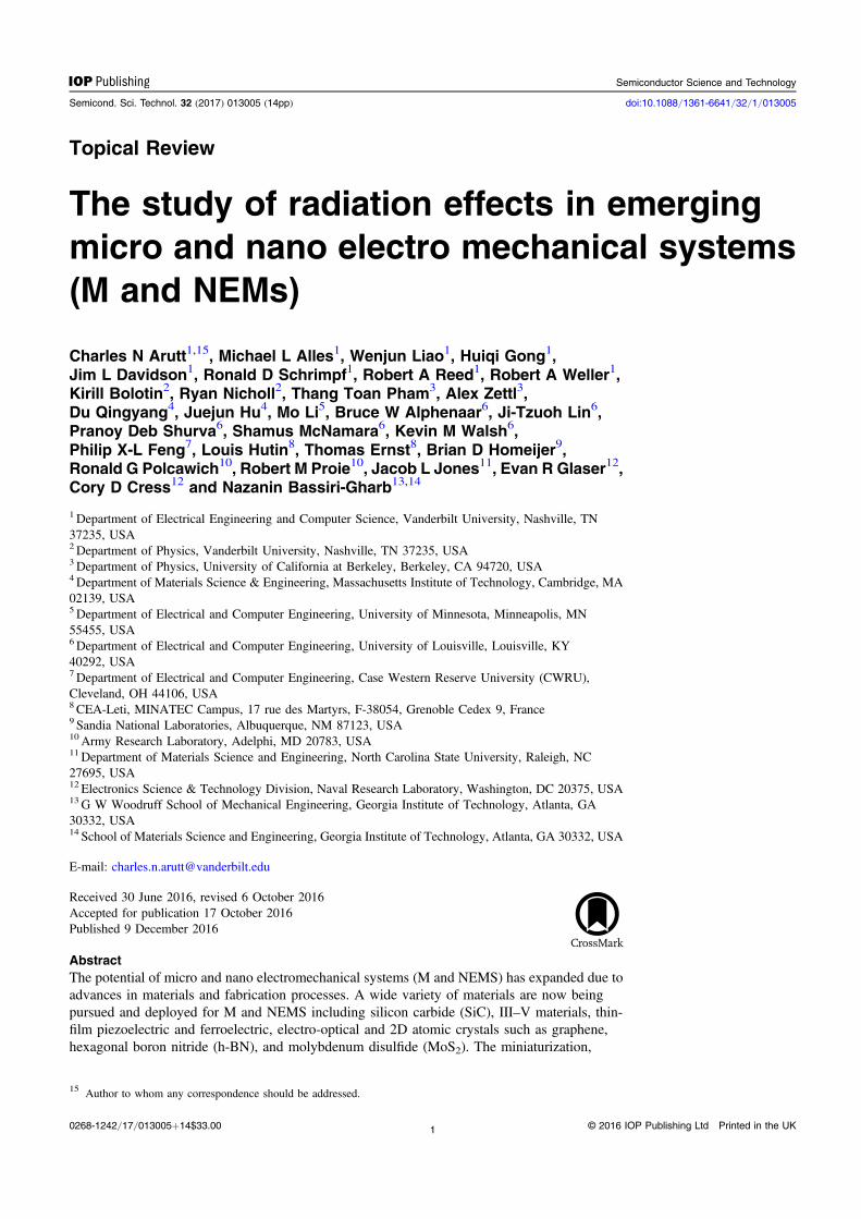
In addition to the aforementioned integration of in-situelectron damage and characterization in a TEM, various otherapproaches are being pursued to enable the in-situ testing ofelectro-mechanical properties with radiation exposure. Oneexample constructed by Vanderbilt researchers is shown infigure 1. In this device, a 2D material is suspended betweentwo long metallic electrodes. These electrodes can be shiftedup and down (thereby straining graphene) by varying thevoltage applied to actuating electrodes A1 and A2. The carrierdensity in graphene can be varied separately, by changing thevoltage on the gate electrode. This device can be probed bothelectrically and using optical techniques to extract electricaland mechanical properties. Presently, electrical probing iswell integrated with radiation sources such as x-ray andgamma ray sources, and particle accelerators, however optical
Figure 1. A platform for simultaneous probing of electrical transportand mechanical properties of 2D materials.
4
Semicond. Sci. Technol. 32 (2017) 013005 Topical Review
characterization is not well integrated and requires ex situmeasurements. This is another test consideration and area ofongoing development.
Another approach to integrating the radiation exposuresand characterization is the use of more conventional siliconmicromachining MEMS techniques to implement a platformthat can be used to manipulate and characterize other mate-rials (e.g. 2DACs), for example within the TEM setup notedearlier. The concept is illustrated in figure 2 and is an area ofongoing collaboration between Sandia National Laboratory,Vanderbilt, and UC Berkeley. One consideration is isolationof the region that is desired for radiation exposure from therest of the platform, for which an aperture exposure from theback-side is the approach.
As noted previously, simulation of radiation interactionswith materials is complex and not readily accessible incommercial software packages compared to simulations of Mand NEMs device operation. For 2DACs, density functionaltheory and kinetic Monte Carlo simulations can be used tosimulate atomic/molecular level interactions such as inter-actions with oxygen [49, 50]. For simulation of displacementdamage due to energetic particles in 2DACs, the commonlyused stopping range on ions in Mmatter (SRIM) package [51]is not applicable. Present research as part of the studiesdescribed in this paper are investigating the application ofMonte Carlo calculations to describe the process of defectgeneration in mono-layer graphene and other 2DACs. Ingeneral, interaction cross sections are very small for mono-layer materials compared to bulk materials, and thus fairlyhigh exposure doses have been reported in the limited studiesto date. Interesting, however, is that from our preliminarycalculations of defect yields, which agree with publishedresults, the indications are that even for ions incident normalto the plane of the 2DAC, the defect generation is dominatedby in-plane, multiple-vacancy events. This is an area ofongoing research.
4. Resonators
MEMS resonators potentially provide a low cost, single-chipalternative to quartz–crystal resonators for clocks or fre-quency references in RF communication systems [52].MEMS resonators can also be used as highly sensitive andselective bio-chemical or gas sensors [53]. MEMS logic andmemory elements can be made from nonlinear resonators inwhich multiple states exist [2, 54].
The resonant properties of M and NEM structures areinherently coupled to the mechanical properties of the mate-rials and dimensions of the fabricated structures. Measure-ment of resonant parameters as a function of radiationexposure is one approach being pursued to explore the impactof radiation on the electro-mechanical properties of con-stituent materials. Examples of structures under investigationinclude suspended silicon cantilevers, suspended SiC canti-levers, thin SiC membranes, GaN cantilevers, 2D graphenemembranes (and other 2D material variants), and 2D materialcantilevers.
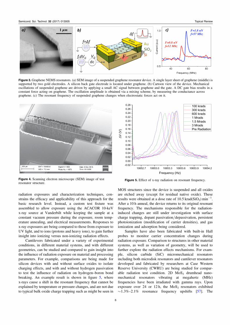
A device structure such as shown in figure 1 can serve asa resonator. Figure 3 illustrates an experimental platformconsisting of monolayer graphene or MoS2 NEM resonatorsthat actuate and read-out. This allows for measurement ofmechanical properties like Young’s modulus. An AC voltageis applied between the 2DAC and an underlying electrode tocreate mechanical oscillations. The amplitude can beobserved electrically by measuring transconductance. Byanalyzing changes of the resonant frequency as a function ofapplied forces, the built-in strain, Young’s modulus, and thethermal expansion coefficient can be measured. Mechanicalbreaking strength of 2DACs can be determined by increasingthe externally applied gate voltage. Since the mechanicalparameters are determined electrically, the test structure canbe integrated with radiation sources to elucidate changes inmechanical properties as a function of radiation exposure.
Another example is a resonator test structure, shown infigure 4, consisting of an electrostatically driven horizontalresonating cantilever fabricated from a silicon-on-insulator(SOI) substrate and employing a piezo-resistive sensingmechanism, developed by researchers at the University ofLouisville [55]. An AC electrostatic excitation causes thecantilever beam to oscillate, and introduces compression andtension on opposite faces of the cantilever base. The resist-ance of the base changes with strain due to the piezoresistivityof the silicon. The beam has an asymmetric design thatmaximizes the voltage difference measured across the deviceunder deflection. During testing, the frequency of the gatevoltage is varied and the voltage output monitored to deter-mine the resonant response of the cantilever. The influence ofradiation exposure on the frequency characteristics can thenbe tested. As with many M and NEMS structures (especiallyresonators) the resonance is sensitive to temperature andpressure, as well as ambient exposure (meaning they need tooperate under vacuum). While there are approaches forencapsulation of silicon MEM structures such as [56], thevariations of geometries and materials of interest, andaccessibility of the material layers of interest for some
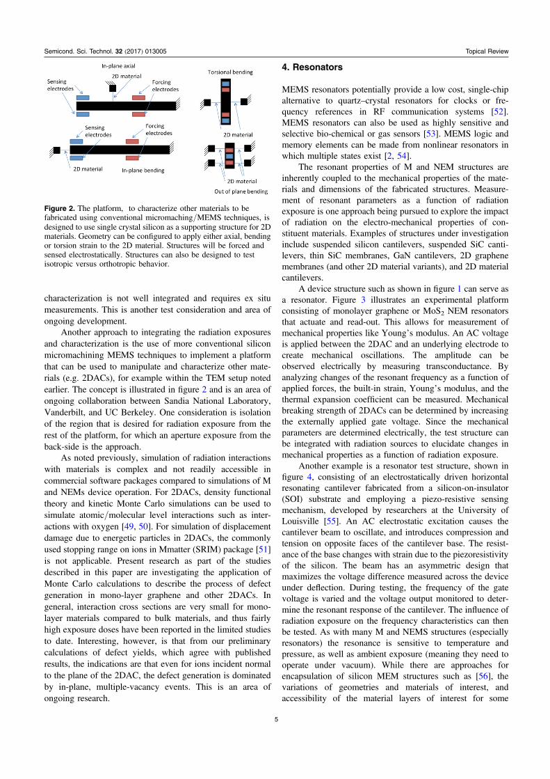
Figure 2. The platform, to characterize other materials to befabricated using conventional micromaching/MEMS techniques, isdesigned to use single crystal silicon as a supporting structure for 2Dmaterials. Geometry can be configured to apply either axial, bendingor torsion strain to the 2D material. Structures will be forced andsensed electrostatically. Structures can also be designed to testisotropic versus orthotropic behavior.
5
Semicond. Sci. Technol. 32 (2017) 013005 Topical Review
radiation exposures and characterization techniques, con-strains the efficacy and applicability of this approach for thebasic research level. Instead, a custom test fixture wasassembled to allow exposure using the ACACOR 10-keVx-ray source at Vanderbilt while keeping the sample at aconstant vacuum pressure during the exposure, room temp-erature annealing, and electrical measurements. Responses tox-ray exposures are being compared to those from exposure toUV light, and to ions (protons and heavy ions), to gain furtherinsight into ionizing versus non-ionizing radiation effects.
Cantilevers fabricated under a variety of experimentalconditions, in different material systems, and with differentgeometries, can be studied and compared to gain insight intothe influence of radiation exposure on material and processingparameters. For example, comparisons are being made forsilicon devices with and without surface oxides to isolatecharging effects, and with and without hydrogen passivationto test the influence of radiation on hydrogen–boron bondbreaking. An example result is shown in figure 5, wherex-rays cause a shift in the resonant frequency that cannot beexplained by temperature or pressure changes, and are not dueto typical bulk oxide charge trapping such as might be seen in
MOS structures since the device is suspended and all oxidesare etched away (except for residual native oxide). Theseresults were obtained at a dose rate of 10.5 krad(SiO2)min−1.After a 10 h anneal, the device returns to its original resonantfrequency. The mechanisms responsible for the radiation-induced changes are still under investigation with surfacecharge trapping, dopant passivation/depassivation, persistentphotoionization (modification of carrier densities), and gasionization and adsorption being considered.
Samples have also been fabricated with built-in Hallprobes to monitor carrier concentration changes duringradiation exposure. Comparison to structures in other materialsystems, as well as variation of geometry, will be used tofurther explore the radiation effects mechanisms. For exam-ple, silicon carbide (SiC) micromechanical resonatorsincluding both microdisk resonators and cantilever resonatorsdeveloped and fabricated by researchers at Case WesternReserve University (CWRU) are being studied for compar-able radiation test condition. 2D MoS2 drumhead nano-mechanical resonators vibrating at megahertz (MHz)frequencies have been irradiated with gamma rays. Uponexposure over 24 or 12 h, the MoS2 resonators exhibited∼1.3%–2.1% resonance frequency upshifts [57]. The
Figure 3.Graphene NEMS resonators. (a) SEM image of a suspended graphene resonator device. A single layer sheet of graphene (middle) issupported by two gold electrodes. A silicon back gate electrode is located under graphene. (b) Cartoon view of the device. Mechanicaloscillations of suspended graphene are driven by applying a small AC signal between graphene and the gate. A DC gate bias results in aconstant force acting on graphene. The oscillation amplitude is obtained via a mixing scheme, by measuring the conductance acrossgraphene. (c) The resonant frequency of suspended graphene changes when electrostatic forces act on it.
Figure 4. Scanning electron microscope (SEM) image of testresonator structure.
Figure 5. Effect of x-ray radiation on resonant frequency.
6
Semicond. Sci. Technol. 32 (2017) 013005 Topical Review
radiation effects observed thus far in SiC microdisk resonatorsand cantilever resonators have been weak, and the variationsof important quantities such as resonance frequencies andquality (Q) factors have been quite small. However, it shouldbe noted that for resonators, even small changes can be sig-nificant since related applications can require much tightercontrol for electronic devices that might be used, for example,in digital logic circuits.
5. Logic switches and gates
The long-term quest for zero-leakage, abrupt switching,ultralow-power logic device has stimulated exploration oflogic switches based on contact-mode NEMS [1, 3, 23, 58–65] and references therein. This has been driven by the fun-damental advantages that NEMS offer, at least including: (i)ideal abrupt switching with zero off-state leakage, (ii) suit-ability for high-temperature operation and potentially in otherharsh or extreme environments (including those in which thedevices are exposed to radiation), and (iii) potential for verysmall footprints. For radiation environments, one of thepotentially most attractive attributes could be an inherentresistance to transient radiation (single-events and photo-currents). Very little work has been done in the study ofradiation effects mechanisms in such devices, in large partdue to the immaturity of the technologies which have sufferedfrom contact failure and reliability issues.
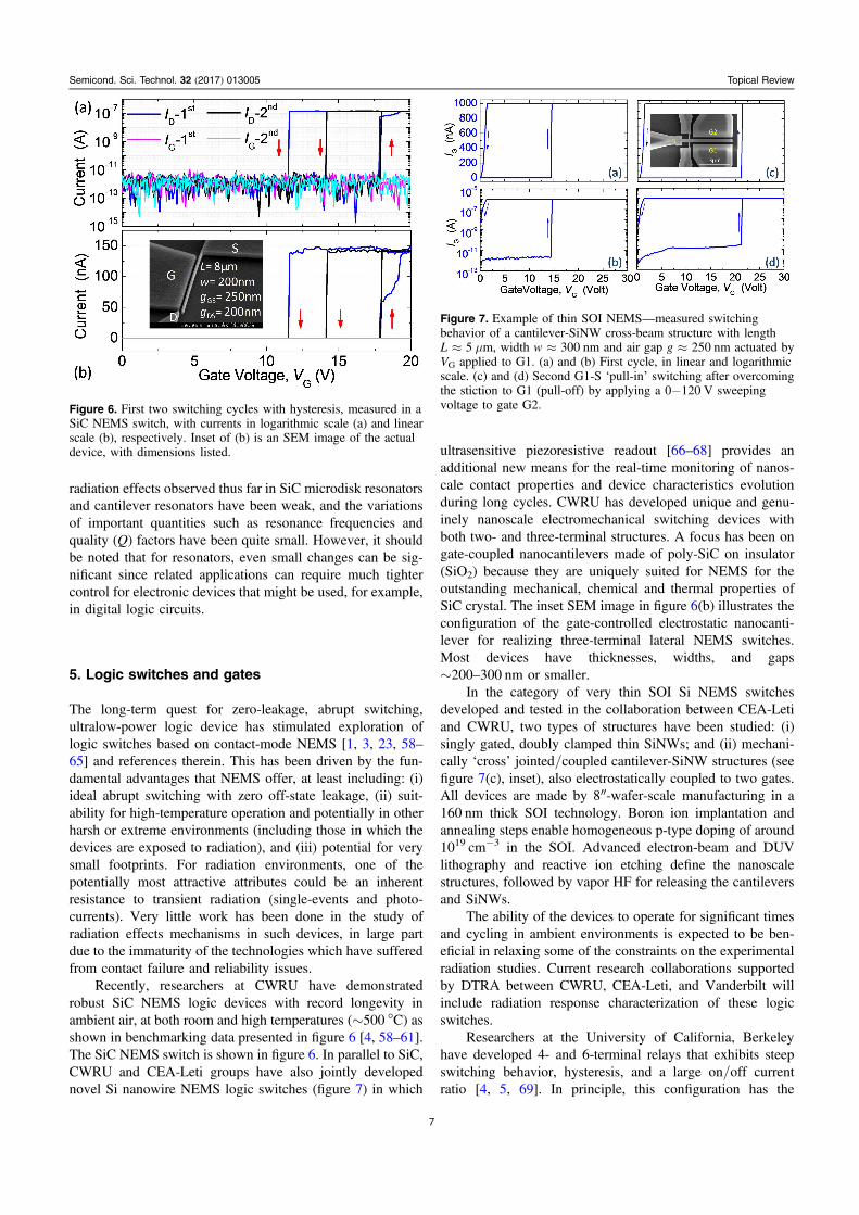
Recently, researchers at CWRU have demonstratedrobust SiC NEMS logic devices with record longevity inambient air, at both room and high temperatures (∼500 °C) asshown in benchmarking data presented in figure 6 [4, 58–61].The SiC NEMS switch is shown in figure 6. In parallel to SiC,CWRU and CEA-Leti groups have also jointly developednovel Si nanowire NEMS logic switches (figure 7) in which
ultrasensitive piezoresistive readout [66–68] provides anadditional new means for the real-time monitoring of nanos-cale contact properties and device characteristics evolutionduring long cycles. CWRU has developed unique and genu-inely nanoscale electromechanical switching devices withboth two- and three-terminal structures. A focus has been ongate-coupled nanocantilevers made of poly-SiC on insulator(SiO2) because they are uniquely suited for NEMS for theoutstanding mechanical, chemical and thermal properties ofSiC crystal. The inset SEM image in figure 6(b) illustrates theconfiguration of the gate-controlled electrostatic nanocanti-lever for realizing three-terminal lateral NEMS switches.Most devices have thicknesses, widths, and gaps∼200–300 nm or smaller.
In the category of very thin SOI Si NEMS switchesdeveloped and tested in the collaboration between CEA-Letiand CWRU, two types of structures have been studied: (i)singly gated, doubly clamped thin SiNWs; and (ii) mechani-cally ‘cross’ jointed/coupled cantilever-SiNW structures (seefigure 7(c), inset), also electrostatically coupled to two gates.All devices are made by 8″-wafer-scale manufacturing in a160 nm thick SOI technology. Boron ion implantation andannealing steps enable homogeneous p-type doping of around1019 cm−3 in the SOI. Advanced electron-beam and DUVlithography and reactive ion etching define the nanoscalestructures, followed by vapor HF for releasing the cantileversand SiNWs.
The ability of the devices to operate for significant timesand cycling in ambient environments is expected to be ben-eficial in relaxing some of the constraints on the experimentalradiation studies. Current research collaborations supportedby DTRA between CWRU, CEA-Leti, and Vanderbilt willinclude radiation response characterization of these logicswitches.
Researchers at the University of California, Berkeleyhave developed 4- and 6-terminal relays that exhibits steepswitching behavior, hysteresis, and a large on/off currentratio [4, 5, 69]. In principle, this configuration has the
Figure 6. First two switching cycles with hysteresis, measured in aSiC NEMS switch, with currents in logarithmic scale (a) and linearscale (b), respectively. Inset of (b) is an SEM image of the actualdevice, with dimensions listed.
Figure 7. Example of thin SOI NEMS—measured switchingbehavior of a cantilever-SiNW cross-beam structure with lengthL≈5 μm, width w≈300 nm and air gap g≈250 nm actuated byVG applied to G1. (a) and (b) First cycle, in linear and logarithmicscale. (c) and (d) Second G1-S ‘pull-in’ switching after overcomingthe stiction to G1 (pull-off) by applying a 0−120 V sweepingvoltage to gate G2.
7
Semicond. Sci. Technol. 32 (2017) 013005 Topical Review
potential to operate at extremely low voltages and may beable to use less energy than CMOS logic [70]. The config-uration allows operation as a combinatorial logic gate (notjust a single switch). These devices currently consist of amoveable body electrode over a fixed gate, drain, and sourcewhere the body is supported by four flexure beams. There is a100 nm air gap between the contacts body electrode and thecontacts on the substrate. These devices are operated byapplying a sufficient voltage between the body and gate[5, 71]. Failure mechanisms of these devices have beenexplored and show that a possible issue could include chargetrapping in the dielectric (Al2O3), a shift in the on and offvoltages over many cycles, and the body being permanentlystuck in the ‘on’ state [69]. Radiation studies have beenlimited by the tendency for oxidation of the metal contactelectrodes, which can cause changes in inherent stiction for-ces if the devices are exposed to atmosphere for extendedperiods, and make it difficult to delineate the impact ofradiation. As with other devices discussed, the need for sto-rage and testing under vacuum is one of the challenges in thestudy of these devices in the current embodiment.
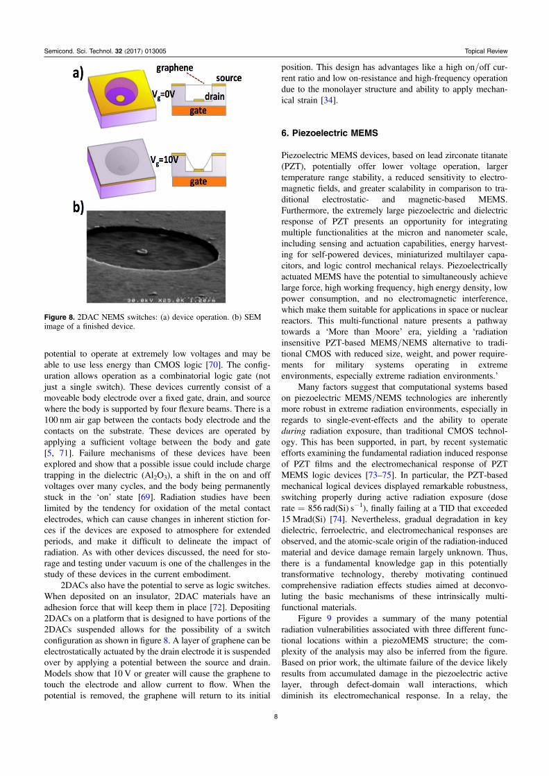
2DACs also have the potential to serve as logic switches.When deposited on an insulator, 2DAC materials have anadhesion force that will keep them in place [72]. Depositing2DACs on a platform that is designed to have portions of the2DACs suspended allows for the possibility of a switchconfiguration as shown in figure 8. A layer of graphene can beelectrostatically actuated by the drain electrode it is suspendedover by applying a potential between the source and drain.Models show that 10 V or greater will cause the graphene totouch the electrode and allow current to flow. When thepotential is removed, the graphene will return to its initial
position. This design has advantages like a high on/off cur-rent ratio and low on-resistance and high-frequency operationdue to the monolayer structure and ability to apply mechan-ical strain [34].
6. Piezoelectric MEMS
Piezoelectric MEMS devices, based on lead zirconate titanate(PZT), potentially offer lower voltage operation, largertemperature range stability, a reduced sensitivity to electro-magnetic fields, and greater scalability in comparison to tra-ditional electrostatic- and magnetic-based MEMS.Furthermore, the extremely large piezoelectric and dielectricresponse of PZT presents an opportunity for integratingmultiple functionalities at the micron and nanometer scale,including sensing and actuation capabilities, energy harvest-ing for self-powered devices, miniaturized multilayer capa-citors, and logic control mechanical relays. Piezoelectricallyactuated MEMS have the potential to simultaneously achievelarge force, high working frequency, high energy density, lowpower consumption, and no electromagnetic interference,which make them suitable for applications in space or nuclearreactors. This multi-functional nature presents a pathwaytowards a ‘More than Moore’ era, yielding a ‘radiationinsensitive PZT-based MEMS/NEMS alternative to tradi-tional CMOS with reduced size, weight, and power require-ments for military systems operating in extremeenvironments, especially extreme radiation environments.’
Many factors suggest that computational systems basedon piezoelectric MEMS/NEMS technologies are inherentlymore robust in extreme radiation environments, especially inregards to single-event-effects and the ability to operateduring radiation exposure, than traditional CMOS technol-ogy. This has been supported, in part, by recent systematicefforts examining the fundamental radiation induced responseof PZT films and the electromechanical response of PZTMEMS logic devices [73–75]. In particular, the PZT-basedmechanical logical devices displayed remarkable robustness,switching properly during active radiation exposure (doserate=856 rad(Si) s−1), finally failing at a TID that exceeded15Mrad(Si) [74]. Nevertheless, gradual degradation in keydielectric, ferroelectric, and electromechanical responses areobserved, and the atomic-scale origin of the radiation-inducedmaterial and device damage remain largely unknown. Thus,there is a fundamental knowledge gap in this potentiallytransformative technology, thereby motivating continuedcomprehensive radiation effects studies aimed at deconvo-luting the basic mechanisms of these intrinsically multi-functional materials.
Figure 9 provides a summary of the many potentialradiation vulnerabilities associated with three different func-tional locations within a piezoMEMS structure; the com-plexity of the analysis may also be inferred from the figure.Based on prior work, the ultimate failure of the device likelyresults from accumulated damage in the piezoelectric activelayer, through defect-domain wall interactions, whichdiminish its electromechanical response. In a relay, the
Figure 8. 2DAC NEMS switches: (a) device operation. (b) SEMimage of a finished device.
8
Semicond. Sci. Technol. 32 (2017) 013005 Topical Review
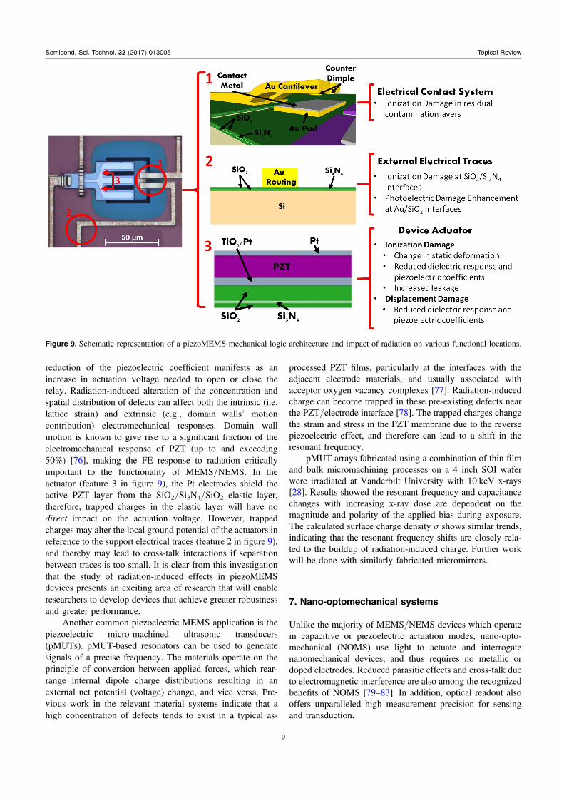
reduction of the piezoelectric coefficient manifests as anincrease in actuation voltage needed to open or close therelay. Radiation-induced alteration of the concentration andspatial distribution of defects can affect both the intrinsic (i.e.lattice strain) and extrinsic (e.g., domain walls’ motioncontribution) electromechanical responses. Domain wallmotion is known to give rise to a significant fraction of theelectromechanical response of PZT (up to and exceeding50%) [76], making the FE response to radiation criticallyimportant to the functionality of MEMS/NEMS. In theactuator (feature 3 in figure 9), the Pt electrodes shield theactive PZT layer from the SiO2/Si3N4/SiO2 elastic layer,therefore, trapped charges in the elastic layer will have nodirect impact on the actuation voltage. However, trappedcharges may alter the local ground potential of the actuators inreference to the support electrical traces (feature 2 in figure 9),and thereby may lead to cross-talk interactions if separationbetween traces is too small. It is clear from this investigationthat the study of radiation-induced effects in piezoMEMSdevices presents an exciting area of research that will enableresearchers to develop devices that achieve greater robustnessand greater performance.
Another common piezoelectric MEMS application is thepiezoelectric micro-machined ultrasonic transducers(pMUTs). pMUT-based resonators can be used to generatesignals of a precise frequency. The materials operate on theprinciple of conversion between applied forces, which rear-range internal dipole charge distributions resulting in anexternal net potential (voltage) change, and vice versa. Pre-vious work in the relevant material systems indicate that ahigh concentration of defects tends to exist in a typical as-
processed PZT films, particularly at the interfaces with theadjacent electrode materials, and usually associated withacceptor oxygen vacancy complexes [77]. Radiation-inducedcharge can become trapped in these pre-existing defects nearthe PZT/electrode interface [78]. The trapped charges changethe strain and stress in the PZT membrane due to the reversepiezoelectric effect, and therefore can lead to a shift in theresonant frequency.
pMUT arrays fabricated using a combination of thin filmand bulk micromachining processes on a 4 inch SOI waferwere irradiated at Vanderbilt University with 10 keV x-rays[28]. Results showed the resonant frequency and capacitancechanges with increasing x-ray dose are dependent on themagnitude and polarity of the applied bias during exposure.The calculated surface charge density σ shows similar trends,indicating that the resonant frequency shifts are closely rela-ted to the buildup of radiation-induced charge. Further workwill be done with similarly fabricated micromirrors.
7. Nano-optomechanical systems
Unlike the majority of MEMS/NEMS devices which operatein capacitive or piezoelectric actuation modes, nano-opto-mechanical (NOMS) use light to actuate and interrogatenanomechanical devices, and thus requires no metallic ordoped electrodes. Reduced parasitic effects and cross-talk dueto electromagnetic interference are also among the recognizedbenefits of NOMS [79–83]. In addition, optical readout alsooffers unparalleled high measurement precision for sensingand transduction.
Figure 9. Schematic representation of a piezoMEMS mechanical logic architecture and impact of radiation on various functional locations.
9
Semicond. Sci. Technol. 32 (2017) 013005 Topical Review

When non-electrical actuation schemes (including opticalmethods) are implemented, radiation-induced mechanicaldegradation of MEMS/NEMS structural materials constitutesthe primary cause of system performance deterioration orbaseline drift. Nevertheless, studies on the impact of structuralmaterial degradation on MEMS/NEMS reliability have onlybeen reported for a small set of materials [15, 17, 19, 74–88]and fundamental insights into the material transformationsthat account for the measured property modification are stilllacking. In this regard, NOMS present unique advantages toisolating mechanical damaging effects caused by radiationand correlate the observed property change with corresp-onding material defect identities.
NOMS allows accurate quantification of radiationdamage caused by intrinsic material mechanical propertychange rather than extrinsic factors such as malfunctioning ofdrive and control electronics which account for manyinstances of radiation-induced MEMS/NEMS failure. Thematerials used in NOMS are relatively simple, including onlyone or at most two types of materials (e.g., Si, SiN, or SiO2)and usually do not involve metals or doped semiconductors.Therefore, the investigation of radiation effect can be focusedon the key structural materials for MEMS/NEMS, avoidingambiguity in interpretation of the results. NOMS interrogationcan be coupled with in situ micro-analytical techniques suchas micro-Raman spectroscopy and correlative light/electronmicroscopy to elucidate the structural origin for measuredproperty variations.
In addition to being a preferred test vehicle to extractgeneral information applicable to MEMS/NEMS materialsand system design, NOMS are anticipated to be a compara-tively radiation resistant platform since they are immune todielectric charging common in M and NEMS failures [7, 16].NOMS sensors can be deployed at the radiation site andmonitored remotely in real-time using optical fibers whileleaving the testing equipment in a radiation-free environment.This configuration is useful for in situ characterization ofNOMS devices during radiation exposure and potentialapplications such as temperature and pressure sensing insidenuclear reactors [89].
Figure 10(a) schematically illustrates an archetypalNOMS testing device consisting of a pair of grating couplersfor light input/output and an optical waveguide. A section ofthe waveguide is suspended from the substrate via undercutetching. Interaction of the optical mode propagating in thewaveguide and the substrate produces a transverse gradientoptical force acting on the waveguide towards the substrate[1]. The use of grating couplers enables a multitude of devicesto be interrogated in parallel using a standard fiber-optic arrayinterface. Figure 10(b) illustrates the device characterizationsetup using a pump-probe configuration. During testing, amodulated pump laser beam is coupled into the waveguidethat generates an optical force to actuate the mechanicaloscillation of the suspended waveguide section. Displacementof the suspended waveguide leads to a spectral shift of Fabry–Perot fringes formed between the input and output gratingcouplers, and the resulting intensity oscillation in the temporaldomain is monitored using a probe laser light. For real-time
tracking of the resonance frequency, a phase-locked loopsetup can be implemented.
To quantify the undamped mechanical resonance fre-quency and quality factor, the measurement is conducted inmoderate vacuum (<10-4 Torr). Since the measured para-meters solely depend on elastic moduli of the waveguidematerial, results obtained from irradiated and as-fabricateddevices can be compared to assess radiation-induced effectsin the waveguide material. However, the radiation-inducedeffect may be submerged by the thermal drift of themechanical resonance frequency. To suppress such noises, thetemperature coefficient of frequency of the devices need to beminimized and accounted for by careful calibration during thestudy. Besides suspended waveguides, other NOMS deviceplatforms including cantilevers, clamped–clamped beams,and torsional paddles can be similarly used for radiationhardness testing to reveal intrinsic material property mod-ifications due to radiation.
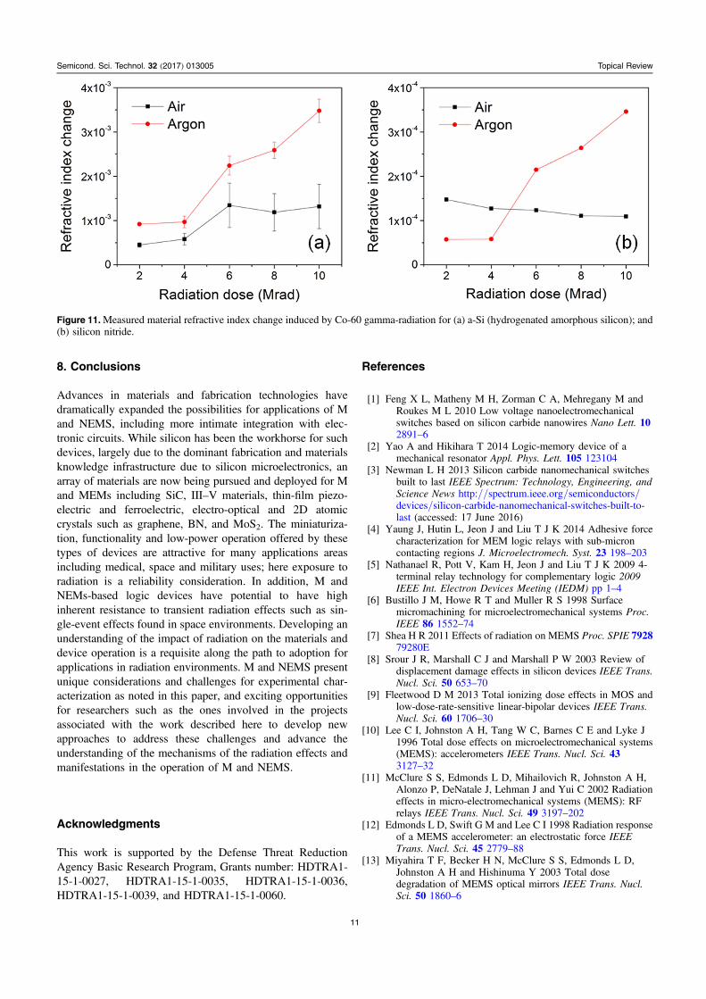
Three structural materials that are ubiquitously used inMEMS/NEMS, namely Si (including a-Si), silicon mono-nitride (SiN) and silicon carbide (SiC) are currently beingtested using the NOMS platform at Massachusetts Institute ofTechnology. All three materials provide high refractive indi-ces and excellent optical transparency in the infrared formaking optical waveguide devices. The optical interrogationmethod has been used to quantify optical refractive indexmodification induced by Co-60 γ-radiation in these materialsas shown in figure 11. In addition, the optical interrogationidentified surface oxidation as the main mechanism account-ing for the observed refractive index change, which is con-firmed by x-ray photoelectron spectroscopy analysis.Characterizations of the material mechanical properties arecurrently underway.
Figure 10. (a) Schematic illustration of a NOMS testing device; (b)block diagram of the NOMS measurement setup.
10
Semicond. Sci. Technol. 32 (2017) 013005 Topical Review
8. Conclusions
Advances in materials and fabrication technologies havedramatically expanded the possibilities for applications of Mand NEMS, including more intimate integration with elec-tronic circuits. While silicon has been the workhorse for suchdevices, largely due to the dominant fabrication and materialsknowledge infrastructure due to silicon microelectronics, anarray of materials are now being pursued and deployed for Mand MEMs including SiC, III–V materials, thin-film piezo-electric and ferroelectric, electro-optical and 2D atomiccrystals such as graphene, BN, and MoS2. The miniaturiza-tion, functionality and low-power operation offered by thesetypes of devices are attractive for many applications areasincluding medical, space and military uses; here exposure toradiation is a reliability consideration. In addition, M andNEMs-based logic devices have potential to have highinherent resistance to transient radiation effects such as sin-gle-event effects found in space environments. Developing anunderstanding of the impact of radiation on the materials anddevice operation is a requisite along the path to adoption forapplications in radiation environments. M and NEMS presentunique considerations and challenges for experimental char-acterization as noted in this paper, and exciting opportunitiesfor researchers such as the ones involved in the projectsassociated with the work described here to develop newapproaches to address these challenges and advance theunderstanding of the mechanisms of the radiation effects andmanifestations in the operation of M and NEMS.
Acknowledgments
This work is supported by the Defense Threat ReductionAgency Basic Research Program, Grants number: HDTRA1-15-1-0027, HDTRA1-15-1-0035, HDTRA1-15-1-0036,HDTRA1-15-1-0039, and HDTRA1-15-1-0060.
References
[1] Feng X L, Matheny M H, Zorman C A, Mehregany M andRoukes M L 2010 Low voltage nanoelectromechanicalswitches based on silicon carbide nanowires Nano Lett. 102891–6
[2] Yao A and Hikihara T 2014 Logic-memory device of amechanical resonator Appl. Phys. Lett. 105 123104
[3] Newman L H 2013 Silicon carbide nanomechanical switchesbuilt to last IEEE Spectrum: Technology, Engineering, andScience News http://spectrum.ieee.org/semiconductors/devices/silicon-carbide-nanomechanical-switches-built-to-last (accessed: 17 June 2016)
[4] Yaung J, Hutin L, Jeon J and Liu T J K 2014 Adhesive forcecharacterization for MEM logic relays with sub-microncontacting regions J. Microelectromech. Syst. 23 198–203
[5] Nathanael R, Pott V, Kam H, Jeon J and Liu T J K 2009 4-terminal relay technology for complementary logic 2009IEEE Int. Electron Devices Meeting (IEDM) pp 1–4
[6] Bustillo J M, Howe R T and Muller R S 1998 Surfacemicromachining for microelectromechanical systems Proc.IEEE 86 1552–74
[7] Shea H R 2011 Effects of radiation on MEMS Proc. SPIE 792879280E
[8] Srour J R, Marshall C J and Marshall P W 2003 Review ofdisplacement damage effects in silicon devices IEEE Trans.Nucl. Sci. 50 653–70
[9] Fleetwood D M 2013 Total ionizing dose effects in MOS andlow-dose-rate-sensitive linear-bipolar devices IEEE Trans.Nucl. Sci. 60 1706–30
[10] Lee C I, Johnston A H, Tang W C, Barnes C E and Lyke J1996 Total dose effects on microelectromechanical systems(MEMS): accelerometers IEEE Trans. Nucl. Sci. 433127–32
[11] McClure S S, Edmonds L D, Mihailovich R, Johnston A H,Alonzo P, DeNatale J, Lehman J and Yui C 2002 Radiationeffects in micro-electromechanical systems (MEMS): RFrelays IEEE Trans. Nucl. Sci. 49 3197–202
[12] Edmonds L D, Swift G M and Lee C I 1998 Radiation responseof a MEMS accelerometer: an electrostatic force IEEETrans. Nucl. Sci. 45 2779–88
[13] Miyahira T F, Becker H N, McClure S S, Edmonds L D,Johnston A H and Hishinuma Y 2003 Total dosedegradation of MEMS optical mirrors IEEE Trans. Nucl.Sci. 50 1860–6
Figure 11.Measured material refractive index change induced by Co-60 gamma-radiation for (a) a-Si (hydrogenated amorphous silicon); and(b) silicon nitride.
11
Semicond. Sci. Technol. 32 (2017) 013005 Topical Review
[14] Knudson A R, Buchner S, McDonald P, Stapor W J,Campbell A B, Grabowski K S, Knies D L, Lewis S andZhao Y 1996 The effects of radiation on MEMSaccelerometers IEEE Trans. Nucl. Sci. 43 3122–6
[15] Bandi T, Polido-Gomes J, Neels A, Dommann A,Marchand L and Shea H R 2013 Proton-radiation toleranceof silicon and SU-8 as structural materials for high-reliabilityMEMS J. Microelectromech. Syst. 22 1395–402
[16] Shea H R 2009 Radiation sensitivity ofmicroelectromechanical system devicesJ. MicroNanolithography MEMS MOEMS 8 031303
[17] Wang L, Tang J and Huang Q A 2011 Gamma irradiationeffects on surface-micromachined polysilicon resonatorsJ. Microelectromech. Syst. 20 1071–3
[18] Buchner S et al 2007 Response of a MEMS microshutteroperating at 60 K to ionizing radiation IEEE Trans. Nucl.Sci. 54 2463–7
[19] Schanwald L P, Schwank J R, Sniegowsi J J, Walsh D S,Smith N F, Peterson K A, Shaneyfelt M R, Winokur P S,Smith J H and Doyle B L 1998 Radiation effects on surfacemicromachined comb drives and microengines IEEE Trans.Nucl. Sci. 45 2789–98
[20] Holbert K E, Nessel J A, McCready S S, Heger A S andHarlow T H 2003 Response of piezoresistive MEMSaccelerometers and pressure transducers to high gamma doseIEEE Trans. Nucl. Sci. 50 1852–9
[21] McCready S S, Harlow T H, Heger A S and Holbert K E 2002Piezoresistive micromechanical transducer operation in apulsed neutron and gamma ray environment 2002 IEEERadiation Effects Data Workshop pp 181–6
[22] Marinaro D G, McMahon P and Wilson A 2008 Protonradiation effects on MEMS silicon strain gauges IEEETrans. Nucl. Sci. 55 1714–8
[23] Feng P X L 2015 NEMS switches: opportunities andchallenges in emerging IC technologies 2015 Int. Conf. onIC Design Technology (ICICDT) pp 1–6
[24] Collaborations to Develop Miniaturization Technologies forSpace Exploration | Nano and Micro Systems | Capabilities |Microdevices Laboratory | NASA Jet Propulsion LaboratoryCalifornia Institute of Technology (Online) available:http://microdevices.jpl.nasa.gov/capabilities/nano-and-micro-systems/miniaturization-technologies.php (accessed:27 June 2016)
[25] Sandia National Laboratories: MicroElectroMechanicalSystems (MEMS) (Online) available: http://sandia.gov/mstc/mems/ (accessed: 27 June 2016)
[26] Novoselov K S, Jiang D, Schedin F, Booth T J,Khotkevich V V, Morozov S V and Geim A K 2005 Two-dimensional atomic crystals Proc. Natl Acad. Sci. USA 10210451–3
[27] Butler S Z et al 2013 Progress, challenges, and opportunities intwo-dimensional materials beyond graphene ACS Nano 72898–926
[28] Liao W, Zhang E X, Alles M L, Zhang C X, Gong H, Ni K,Sternberg A L, Fleetwood D M, Reed R A andSchrimpf R D Total ionizing dose effects on piezoelectricmicromachined ultrasonic transducers IEEE Trans. Nucl.Sci. accepted
[29] Gong H et al Total-ionizing-dose effects in piezoresistivemicromachined cantilevers IEEE Trans. Nucl. Sci. accepted
[30] Blondy P, Crunteanu A, Pothier A, Tristant P,Catherinot A and Champeaux C 2007 Effects of atmosphereon the reliability of RF-MEMS capacitive switchesMicrowave Conf., 2007 (European, Munich) pp 1346–8
[31] Lamhamdi M, Pons P, Zaghloul U, Boudou L, Coccetti F,Guastavino J, Segui Y, Papaioannou G and Plana R 2008Voltage and temperature effect on dielectric charging forRF-MEMS capacitive switches reliability investigationMicroelectron. Reliabil. 48 1248–52
[32] Lee C, Wei X, Kysar J W and Hone J 2008 Measurement of theelastic properties and intrinsic strength of monolayergraphene Science 321 385–8
[33] Castellanos-Gomez A, Poot M, Steele G A, van der Zant H S J,Agraït N and Rubio-Bollinger G 2012 Elastic properties offreely suspended MoS2 nanosheets Adv. Mater. 24 772–5
[34] Chen C, Lee S, Deshpande V V, Lee G-H, Lekas M,Shepard K and Hone J 2013 Graphene mechanicaloscillators with tunable frequency Nat. Nanotechnol. 8923–7
[35] Zhou Q and Zettl A 2013 Electrostatic graphene loudspeakerAppl. Phys. Lett. 102 223109
[36] Jensen K, Weldon J, Garcia H and Zettl A 2007 Nanotuberadio Nano Lett. 7 3508–11
[37] Jensen K, Kim K and Zettl A 2008 An atomic-resolutionnanomechanical mass sensor Nat. Nanotechnol. 3 533–7
[38] Zhang C X, Zhang E X, Fleetwood D M, Alles M L,Schrimpf R D, Song E B, Galatsis K, Newaz A K M andBolotin K I 2013 Total ionizing dose effects and reliabilityof graphene-based non-volatile memory devices 2013 IEEEAerospace Conf. pp 1–8
[39] Zhang C X, Zhang E X, Fleetwood D M, Alles M L,Schrimpf R D, Song E B, Kim S M, Galatsis K andWang K L W 2012 Electrical stress and total ionizing doseeffects on graphene-based non-volatile memory devicesIEEE Trans. Nucl. Sci. 59 2974–8
[40] Banhart F, Kotakoski J and Krasheninnikov A V 2011Structural defects in graphene ACS Nano 5 26–41
[41] Chang C W, Okawa D, Garcia H, Majumdar A and Zettl A2007 Nanotube phonon waveguide Phys. Rev. Lett. 99045901
[42] Demczyk B G, Wang Y M, Cumings J, Hetman M, Han W,Zettl A and Ritchie R O 2002 Direct mechanicalmeasurement of the tensile strength and elastic modulus ofmultiwalled carbon nanotubes Mater. Sci. Eng. A 334173–8
[43] Jensen J 2007 Static and dynamic Jahn–Teller effects andantiferromagnetic order in PrO2: a mean-field analysis Phys.Rev. B 76 144428
[44] Pham T, Gibb A L, Gilbert S M, Song C and Zettl A 2016Formation and dynamics of electron-irradiation-induceddefects in hexagonal boron nitride at elevated temperaturesMaterials Research Society Spring Meeting (Phoenix,Arizona) (Spring) presented at the
[45] Liu K et al 2015 Self-passivation of defects: effects of high-energy particle irradiation on the elastic modulus ofmultilayer graphene Adv. Mater. 27 6841–7
[46] Nicholl R J T, Conley H J, Lavrik N V, Vlassiouk I,Puzyrev Y S, Sreenivas V P, Pantelides S T and Bolotin K I2015 The effect of intrinsic crumpling on the mechanics offree-standing graphene Nat. Commun. 6 8789
[47] Ruiz-Vargas C S, Zhuang H L, Huang P Y,van der Zande A M, Garg S, McEuen P L, Muller D A,Hennig R G and Park J 2011 Softened elastic response andunzipping in chemical vapor deposition graphenemembranes Nano Lett. 11 2259–63
[48] Cançado L G, Jorio A, Ferreira E H M, Stavale F, Achete C A,Capaz R B, Moutinho M V O, Lombardo A,Kulmala T S and Ferrari A C 2011 Quantifying defects ingraphene via Raman spectroscopy at different excitationenergies Nano Lett. 11 3190–6
[49] Puzyrev Y S, Wang B, Zhang E X, Zhang C X, Newaz A K M,Bolotin K I, Fleetwood D M, Schrimpf R D andPantelides S T 2012 Surface reactions and defect formationin irradiated graphene devices IEEE Trans. Nucl. Sci. 593039–44
[50] Zhang E X, Newaz A K M, Wang B, Zhang C X,Fleetwood D M, Bolotin K I, Schrimpf R D,Pantelides S T and Alles M L 2012 Ozone-exposure and
12
Semicond. Sci. Technol. 32 (2017) 013005 Topical Review
annealing effects on graphene-on-SiO2 transistors Appl.Phys. Lett. 101 121601
[51] James Ziegler—SRIM & TRIM (Online) available: http://srim.org/ (accessed: 27 June 2016)
[52] Uranga A, Verd J and Barniol N 2015 CMOS–MEMSresonators: from devices to applications Microelectron. Eng.132 58–73
[53] Waggoner P S and Craighead H G 2007 Micro- andnanomechanical sensors for environmental, chemical, andbiological detection Lab. Chip 7 1238–55
[54] Xu Y, Lin J-T, Alphenaar B W and Keynton R S 2006 Viscousdamping of microresonators for gas composition analysisAppl. Phys. Lett. 88 143513
[55] Shurva P D, McNamara S, Lin J T, Alphenaar B, Walsh K andDavidson J Axial asymmetry for improved sensitivity inMEMS piezoresistors J. Micromech. Microeng. 26 095014
[56] Stanford Micro Structures Sensors Lab (Online) available:http://micromachine.stanford.edu/?p=projects&id=17(accessed: 27 June 2016)
[57] Lee J, Krupcale M J and Feng P X-L 2016 Effects of γ-rayradiation on two-dimensional molybdenum disulfide (MoS2)nanomechanical resonators Appl. Phys. Lett. 108 023106
[58] He T, Yang R, Ranganathan V, Rajgopal S, Tupta M A,Bhunia S, Mehregany M and Feng P X L 2013 Siliconcarbide (SiC) nanoelectromechanical switches and logicgates with long cycles and robust performance in ambient airand at high temperature 2013 IEEE Int. Electron DevicesMeeting pp 1–4
[59] Engineering researchers report on nanoscale energy-efficientswitching devices ScienceDaily (Online) available: https://sciencedaily.com/releases/2013/12/131209160811.htm(accessed: 17 June 2016)
[60] He T, Yang R, Rajgopal S, Tupta M A, Bhunia S,Mehregany M and Feng P X L 2013 Robust silicon carbide(SiC) nanoelectromechanical switches with long cycles inambient and high temperature conditions 2013 IEEE 26thInt. Conf. on Micro Electro Mechanical Systems (MEMS)pp 516–9
[61] He T, Ranganathan V, Yang R, Rajgopal S, Bhunia S,Mehregany M and Feng P X L 2013 Time-domain ACcharacterization of silicon carbide (SiC)nanoelectromechanical switches toward high-speedoperations 2013 Transducers Eurosensors XXVII: The 17thInt. Conf. on Solid-State Sensors, Actuators andMicrosystems (TRANSDUCERS EUROSENSORS XXVII)pp 669–72
[62] Feng X L, Matheny M H, Karabalin R B, Zorman C A,Mehregany M and Roukes M L 2009 Silicon carbide (SiC)top-down nanowire electromechanical resonatorsTRANSDUCERS 2009–2009 Int. Solid-State Sensors,Actuators and Microsystems Conf. pp 2246–9
[63] Feng X-L, Karabalin R B, Aldridge J S and Roukes M L 2012Nano-electro-mechanical systems switches US PatentUS8258899 B2
[64] Feng P X-L, Matheny M, Karbalin R and Roukes M L 2012Very low voltage, ultrafast nanoelectromechanical switchesand resonant switches US Patent US8115344 B2
[65] He T, Yang R, Rajgopal S, Bhunia S, Mehregany M andFeng P X L 2013 Dual-gate silicon carbide (SiC) lateralnanoelectromechanical switches 2013 8th IEEE Int. Conf. onNano/Micro Engineered and Molecular Systems (NEMS)pp 554–7
[66] Yang R, He T, Marcoux C, Andreucci P, Duraffourg L andFeng P X L 2013 Silicon nanowire and cantileverelectromechanical switches with integrated piezoresistivetransducers 2013 IEEE 26th Int. Conf. on Micro ElectroMechanical Systems (MEMS) pp 229–32
[67] Koumela A, Hentz S, Mercier D, Dupré C, Ollier E,Feng P X-L, Purcell S T and Duraffourg L 2013 High
frequency top-down junction-less silicon nanowireresonators Nanotechnology 24 435203
[68] Yang R, He T, Tupta M A, Marcoux C, Andreucci P,Duraffourg L and Feng P X-L 2015 Probing contact-modecharacteristics of silicon nanowire electromechanicalsystems with embedded piezoresistive transducersJ. Micromech. Microeng. 25 095014
[69] Chen Y, Nathanael R, Yaung J, Hutin L and King Liu T-J 2013Reliability of MEM Relays for Zero Leakage Logic vol 8614,pp 861404–861404–7
[70] Kam H, Liu T J K, Stojanovi V, Markovic D and Alon E 2011Design, optimization, and scaling of MEM relays for ultra-low-power digital logic IEEE Trans. Electron Devices 58236–50
[71] Qian C, Peschot A, Chen I R, Chen Y, Xu N and Liu T J K2015 Effect of body biasing on the energy-delayperformance of logic relays IEEE Electron Device Lett. 36862–4
[72] Conley H, Lavrik N V, Prasai D and Bolotin K I 2011Graphene bimetallic-like cantilevers: probing graphene/substrate interactions Nano Lett. 11 4748–52
[73] Bastani Y, Cortes-Pena A Y, Wilson A D, Gerardin S,Bagatin M, Paccagnella A and Bassiri-Gharb N 2013 Effectsof high energy x ray and proton irradiation on lead zirconatetitanate thin films’ dielectric and piezoelectric response Appl.Phys. Lett. 102 192906
[74] Proie R M, Polcawich R G, Cress C D, Sanchez L M,Grobicki A D, Pulskamp J S and Roche N J H 2013 Totalionizing dose effects in piezoelectric MEMS relays IEEETrans. Nucl. Sci. 60 4505–11
[75] Brewer S J et al 2016 Effect of top electrode material onradiation-induced degradation of ferroelectric thin filmstructures J. Appl. Phys. 12 24101
[76] Bassiri‐Gharb N, Fujii I, Hong E, Trolier‐Mckinstry S,Taylor D V and Damjanovic D 2007 Domain wallcontributions to the properties of piezoelectric thin filmsJ. Electroceram. 19 47–65
[77] Benedetto J M, Moore R A, McLean F B, Brody P S andDey S K 1990 The effect of ionizing radiation on sol-gelferroelectric PZT capacitors IEEE Trans. Nucl. Sci. 371713–7
[78] Schwank J R, Nasby R D, Miller S L, Rodgers M S andDressendorfer P V 1990 Total-dose radiation-induceddegradation of thin film ferroelectric capacitors IEEE Trans.Nucl. Sci. 37 1703–12
[79] Marquardt F and Girvin S M 2009 Optomechanics Physics2 40
[80] Kippenberg T J and Vahala K J 2008 Cavity optomechanics:back-action at the mesoscale Science 321 1172–6
[81] Li M, Pernice W H P, Xiong C, Baehr-Jones T,Hochberg M and Tang H X 2008 Harnessing optical forcesin integrated photonic circuits Nature 456 480–4
[82] Li M, Pernice W H P and Tang H X 2009 Broadband all-photonic transduction of nanocantilevers Nat. Nanotechnol.4 377–82
[83] Li M, Pernice W H P and Tang H X 2010 Ultrahigh-frequencynano-optomechanical resonators in slot waveguide ringcavities Appl. Phys. Lett. 97 183110
[84] Tazzoli A, Cellere G, Autizi E, Peretti V, Paccagnella A andMeneghesso G 2009 Radiation sensitivity of ohmic RF-MEMS switches for spatial applications IEEE 22nd Int.Conf. on Micro Electro Mechanical Systems, 2009. MEMS2009 pp 634–7
[85] Gomes J and Shea H R 2011 Displacement damage effects insilicon MEMS at high proton doses Proc. SPIE 792879280G
[86] Niklaus M, Rosset S and Shea H 2010 Array of lenses withindividually tunable focal-length based on transparent ion-implanted EAPs Proc. SPIE 7642 76422K
13
Semicond. Sci. Technol. 32 (2017) 013005 Topical Review
[87] Gkotsis P, Kilchytska V, Fragkiadakis C, Kirby P B,Raskin J P and Francis L A 2012 Effects of fast neutronson the electromechanical properties of materialsused in microsystems J. Microelectromech. Syst. 211471–83
[88] Wang L, Tang J and Huang Q-A 2012 Gamma and electronbeam irradiation effects on the resistance of micromachined
polycrystalline silicon beams Sensors Actuators Phys. 17799–104
[89] Fernandez A F, Gusarov A I, Brichard B, Bodart S,Lammens K, Berghmans F, Decréton M, Mégret P,Blondel M and Delchambre A 2002 Temperature monitoringof nuclear reactor cores with multiplexed fiber Bragg gratingsensors Opt. Eng. 41 1246–54
14
Semicond. Sci. Technol. 32 (2017) 013005 Topical Review