programme - journées scope 2017 - … · programme . 10h30 - 12h 12h15 ... both these results ......
TRANSCRIPT
4èmes journées de la société française des Semi-Conducteurs et Oxydes Poreux (SCOPe)
22 et 23 juin 2017 - Institut d’Electronique, de Microélectronique et de Nanotechnologie (IEMN)
Villeneuve d’Ascq
PROGRAMME
10h30 - 12h
12h15 - 13h45
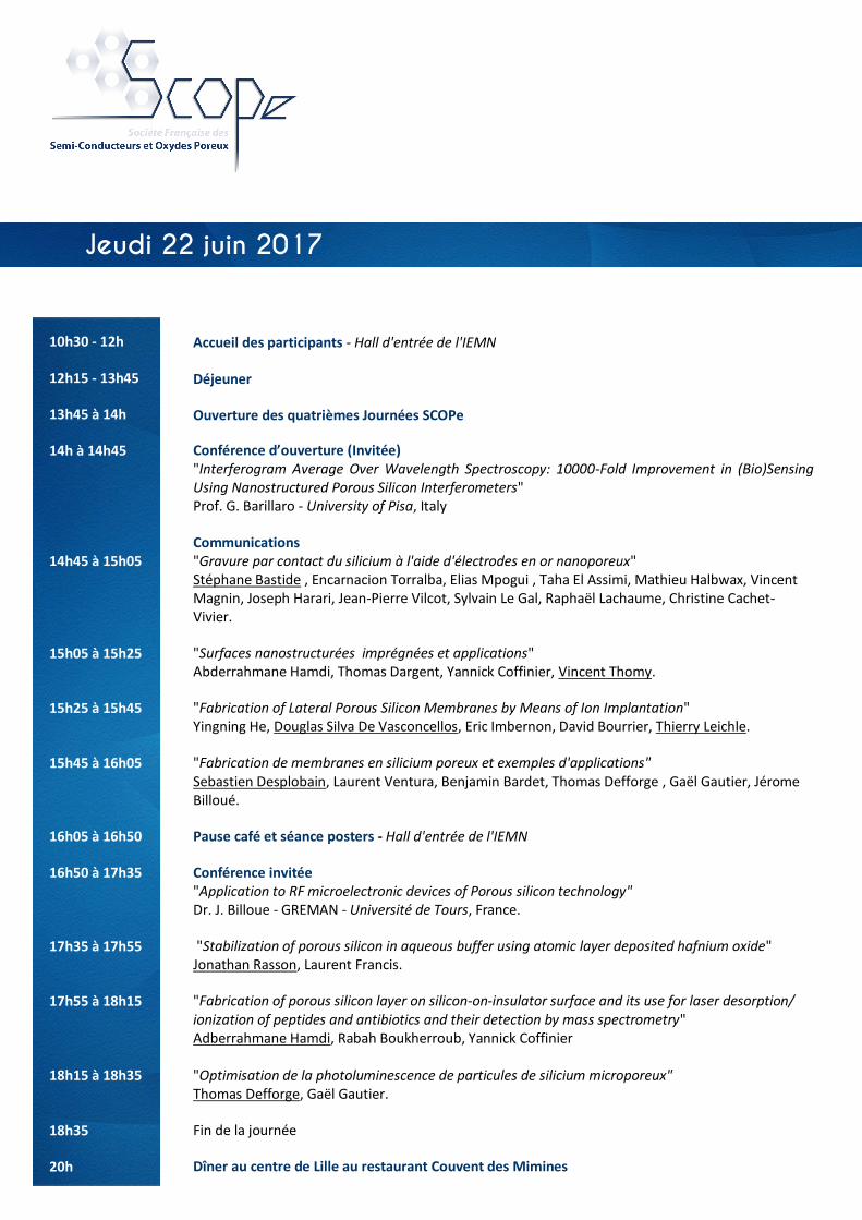
13h45 à 14h
14h à 14h45
14h45 à 15h05
15h05 à 15h25
15h25 à 15h45
15h45 à 16h05
16h05 à 16h50
16h50 à 17h35
17h35 à 17h55
17h55 à 18h15 18h15 à 18h35
18h35
20h
Accueil des participants - Hall d'entrée de l'IEMN
Déjeuner
Ouverture des quatrièmes Journées SCOPe
Conférence d’ouverture (Invitée) "Interferogram Average Over Wavelength Spectroscopy: 10000-Fold Improvement in (Bio)Sensing Using Nanostructured Porous Silicon Interferometers" Prof. G. Barillaro - University of Pisa, Italy
Communications "Gravure par contact du silicium à l'aide d'électrodes en or nanoporeux" Stéphane Bastide , Encarnacion Torralba, Elias Mpogui , Taha El Assimi, Mathieu Halbwax, Vincent Magnin, Joseph Harari, Jean-Pierre Vilcot, Sylvain Le Gal, Raphaël Lachaume, Christine Cachet-Vivier.
"Surfaces nanostructurées imprégnées et applications" Abderrahmane Hamdi, Thomas Dargent, Yannick Coffinier, Vincent Thomy.
"Fabrication of Lateral Porous Silicon Membranes by Means of Ion Implantation" Yingning He, Douglas Silva De Vasconcellos, Eric Imbernon, David Bourrier, Thierry Leichle.
"Fabrication de membranes en silicium poreux et exemples d'applications" Sebastien Desplobain, Laurent Ventura, Benjamin Bardet, Thomas Defforge , Gaël Gautier, Jérome Billoué.
Pause café et séance posters - Hall d'entrée de l'IEMN
Conférence invitée "Application to RF microelectronic devices of Porous silicon technology" Dr. J. Billoue - GREMAN - Université de Tours, France.
"Stabilization of porous silicon in aqueous buffer using atomic layer deposited hafnium oxide" Jonathan Rasson, Laurent Francis.
"Fabrication of porous silicon layer on silicon-on-insulator surface and its use for laser desorption/ionization of peptides and antibiotics and their detection by mass spectrometry" Adberrahmane Hamdi, Rabah Boukherroub, Yannick Coffinier "Optimisation de la photoluminescence de particules de silicium microporeux" Thomas Defforge, Gaël Gautier.
Fin de la journée
Dîner au centre de Lille au restaurant Couvent des Mimines
Jeudi 22 juin 2017
9h15 - 10h
10h - 10h20
10h20 à 10h40 10h40 à 11h10
11h10 à 11h30
11h30 à 11h50
11h50 à 12h30
12h30 à 12h45
12h45 à 14h
Conférence d’ouverture (Invitée) "Matériaux carbonés poreux et leurs applications" Dr. R. Boukherroub - Université de Lille 1, France
Communications "Manufacture and development of all-solid-state Li-ion micro battery based on nanostructured materials" Yasemin Duygu Yucel
"Investigation of the acoustic properties of porous silicon layers used as backing material for Capacitive Micromachined Ultrasonic Transducers" Julie Lascaud
Pause café - Hall d'entrée de l'IEMN
"Porous Silicon Nanoparticles for Cancer Theragnostic" Eduardo Cueto Diaz "Nanotopography of porous silicon scaffold to increase bone regeneration" Naveen Fatima, Elodie Middendorp, Eduardo Jose Cueto Diaz, Alban Desoutter Hamideh Salehi, Frédérique Cunin, Frédéric Cuisinier, Pierre-Yves Collart Dutilleul.
Assemblée Générale de SCOPe.
Remise du prix de la meilleure communication et clôture des 4èmes Journées SCOPe.
Cocktail déjeunatoire - Salle Pierre Armand - IEMN
Vendredi 23 juin 2017
4èmes journées de la société française des Semi-Conducteurs et Oxydes Poreux (SCOPe)
22 et 23 juin 2017 - Institut d’Electronique, de Microélectronique et de Nanotechnologie (IEMN)
Villeneuve d’Ascq
CONFÉRENCIERS INVITÉS

Abstract Porous silicon (PSi) is a nanostructured material increasingly exploited for both refractometric and (bio)sensing applications, though currently suffering of restricted real applications due to insufficient sensitivity and, in turn, poor limit of detection. In this talk, development, characterization, and application (to both refractometry and biosensing) of a novel ultrasensitive technique for the label-free discrimination of either bulk or surface refractive index changes (namely, Interferogram Average over Wavelength – IAW –reflectance spectroscopy) using nanostructured PSi interferometer is discussed. As to refractometric applications, a minimum bulk refraction index variation of 10-7 RIU was experimentally measured using NaCl aqueous solutions, with a theoretical limit of detection of 10-8 RIU. As to biosensing applications, a minimum concentration of TNFα, a protein biomarker of inflammation and sepsis, at concentration of 3 nM was experimentally monitored, with high selectivity and limit of detection of 200 pM. Both these results represent a 1000-fold improvement with respect to the commonly used fast Fourier Transform reflectance spectroscopy for PSi interferometers. The IAW reflectance spectroscopy envisages bringing PSi optical (bio)sensors at the forefront of ultrasensitive label-free biosensing techniques with ultimate limit of detection in the order of pM level. This enables porous silicon targeting real application for point-of-care clinical analysis where low analyte concentrations are required to be detected in small volume of biological samples.
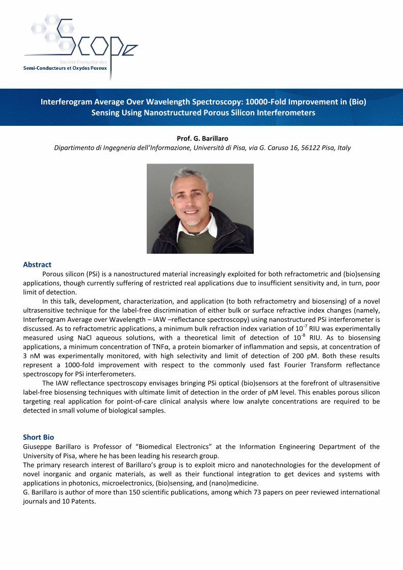
Short Bio Giuseppe Barillaro is Professor of “Biomedical Electronics” at the Information Engineering Department of the University of Pisa, where he has been leading his research group. The primary research interest of Barillaro’s group is to exploit micro and nanotechnologies for the development of novel inorganic and organic materials, as well as their functional integration to get devices and systems with applications in photonics, microelectronics, (bio)sensing, and (nano)medicine. G. Barillaro is author of more than 150 scientific publications, among which 73 papers on peer reviewed international journals and 10 Patents.
Interferogram Average Over Wavelength Spectroscopy: 10000-Fold Improvement in (Bio)Sensing Using Nanostructured Porous Silicon Interferometers
Prof. G. Barillaro Dipartimento di Ingegneria dell’Informazione, Università di Pisa, via G. Caruso 16, 56122 Pisa, Italy
Abstract La première utilisation connue de solides poreux concerne le charbon actif et remonte à l'Antiquité, période durant laquelle les Égyptiens s'en servaient comme adsorbant pour des applications médicales. Depuis, l’intérêt pour les matériaux carbonés poreux n’a cessé de croître pour diverses applications et particulièrement celles liées à la catalyse hétérogène, la séparation sélective de gaz, la purification de l’eau, le stockage énergétique (supercondensateur)... La dernière décennie a vu l’émergence du graphène, un matériau constitué d’une unique couche de carbone. Ce matériau présente des caractéristiques exceptionnelles telles qu’une grande robustesse, une bonne conduction électrique mais aussi une grande surface spécifique. Cette dernière est très importante pour de nombreuses applications où l’interaction avec le matériau est primordiale, dans le cas par exemple des capteurs, supercapacités, relargage de principes actifs, catalyse… Dans cette présentation, je vais discuter les résultats obtenus au laboratoire sur la préparation de matériaux hybrides poreux à base de graphène ou de graphène poreux ainsi que leurs applications dans les domaines de l’environnement, énergie et biomédical. 1. Facile synthesis of fluorinated polydopamine/chitosan/reduced graphene oxide composite aerogel for efficient oil/water separation. Ning Cao, Qian Lyu, Jin Li, Yong Wang, Bai Yang, Sabine Szunerits, Rabah Boukherroub. Chemical Engineering Journal 326 (2017) 17-28 2. Photothermally triggered On-Demand Insulin Release from Reduced Graphene Oxide modified Hydrogels. Florina Teodorescu, Yavuz Oz, Gurvan Quéniat, Amar Abderrahmani, Catherine Foulon, Marie Lecoeur, Rana Sanyal, Amitav Sanyal, Rabah Boukherroub and Sabine Szunerits. Journal of Controlled Release 246 (2017) 164–173 3. On demand electrochemical release of drugs from porous reduced graphene oxide modified flexible electrodes. Samia Boulahneche, Roxana Jijie, Alexandre Barras, Fereshteh Chekin, Florina Teodorescu, Santosh K. Singh, Julie Bouckaert, Mohamed Salah Medjram, Sreekumar Kurungot, Rabah Boukherroub and Sabine Szunerits. Journal of Materials Chemistry B (in press) 4. N-doped Porous Reduced Graphene Oxide as an Efficient Electrode Material for High Performance Flexible Solid-state Supercapacitor. Santosh K. Singh, Vishal M. Dhavale, Rabah Boukherroub, Sreekumar Kurungot and Sabine Szunerits. Applied Materials Today (in press)
Matériaux carbonés poreux : préparation et applications
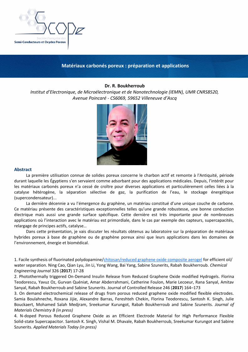
Dr. R. Boukherroub Institut d’Electronique, de Microélectronique et de Nanotechnologie (IEMN), UMR CNRS8520,
Avenue Poincaré - CS6069, 59652 Villeneuve d’Ascq
Abstract The increasing expansion of telecommunication applications leads to the integration of complete system-on chip (SOC) associating analog and digital processing units. Such integrated circuits (IC) involve active devices (diodes or transistors for example) as well as passive components (inductors and/or capacitors), required in many applications as amplifiers, mixers, voltage-controlled oscillators, filters or resonators. Moreover, passive component performances are limited by the proximity of lossy Si substrate and surrounding metallization. Then, obviously, the characteristics of the substrate become crucial to reach high performances of monolithic RF system. Looking for IC compatible processes, porous silicon (PS) seems to be a promising candidate as it can provide localized isolating regions from various silicon substrates. In this work, we present a fan of porous silicon substrates which can be used for RF devices integration. We will put the emphasis on the intrinsic electrical properties such as the AC electrical conductivity or the dielectric constant. Then, we will describe the performances of widespread RF devices, that is to say inductors or coplanar waveguides. Finally, we will describe implementation of more complex functions like passive and active filters.
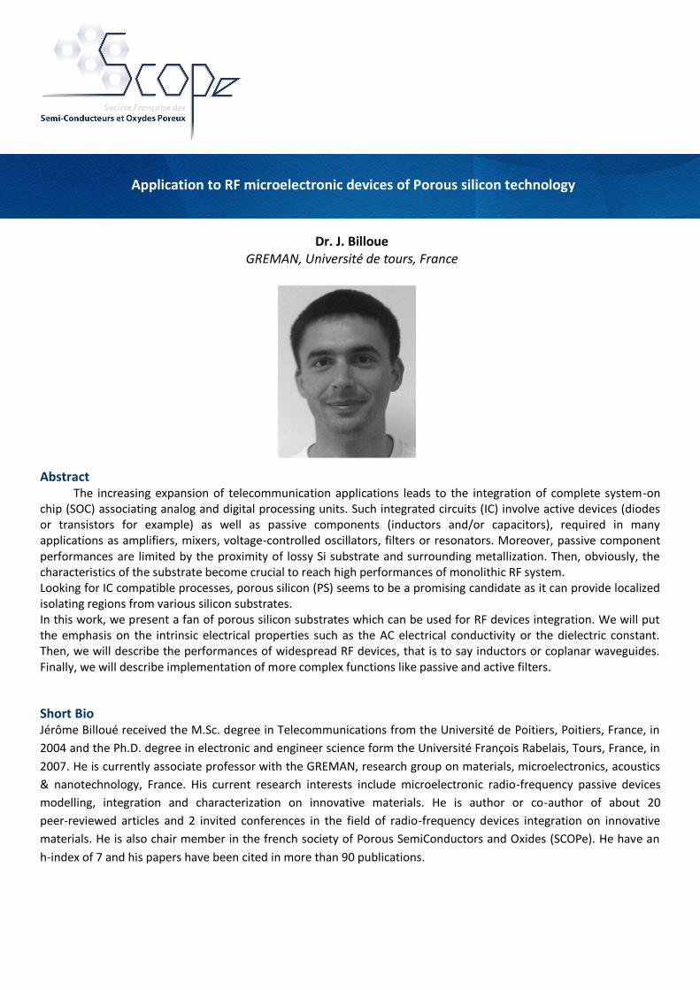
Short Bio Jérôme Billoué received the M.Sc. degree in Telecommunications from the Université de Poitiers, Poitiers, France, in
2004 and the Ph.D. degree in electronic and engineer science form the Université François Rabelais, Tours, France, in
2007. He is currently associate professor with the GREMAN, research group on materials, microelectronics, acoustics
& nanotechnology, France. His current research interests include microelectronic radio-frequency passive devices
modelling, integration and characterization on innovative materials. He is author or co-author of about 20
peer-reviewed articles and 2 invited conferences in the field of radio-frequency devices integration on innovative
materials. He is also chair member in the french society of Porous SemiConductors and Oxides (SCOPe). He have an
h-index of 7 and his papers have been cited in more than 90 publications.
Dr. J. Billoue GREMAN, Université de tours, France
Application to RF microelectronic devices of Porous silicon technology
4èmes journées de la société française des Semi-Conducteurs et Oxydes Poreux (SCOPe)
22 et 23 juin 2017 - Institut d’Electronique, de Microélectronique et de Nanotechnologie (IEMN)
Villeneuve d’Ascq
RECUEIL DE RÉSUMÉS DES PRÉSENTATIONS ORALES
Gravure par contact du silicium à l’aide d’électrodes en or nanoporeux
E. Torralba*, M. Halbwax
**, E. Mpogui
*, T. El Assimi
*, V. Magnin
**, J. Harari
**, J.-P. Vilcot
**,
S. Le Gall***
, R. Lachaume***
, C. Cachet-Vivier*, S. Bastide
*
*Institut de Chimie et des Matériaux Paris-Est, CNRS, U. Paris-Est, France – [email protected]
**Institut d’Électronique, Microélectronique et Nanotechnologies, CNRS, U. Lille 1 – [email protected]
***Génie Électrique et Électronique de Paris, CNRS, SUPELEC, U. Paris-Sud XI – [email protected]
La gravure du silicium (Si) est un processus clé dans la fabrication de microstructures essentielles pour plusieurs
familles de composants utilisées en microélectronique, photonique ou pour les laboratoires sur puces. Une grande variété
de technologies de microstructuration de Si existe de nos jours. Leur efficacité remarquable nécessite néanmoins de
nombreuses étapes de traitement (masquage / lithographie par faisceau de photon ou électron / gravures humides ou
sèches) qui ne conviennent pas à toutes les industries, notamment lorsque la réduction des coûts et les cadences de
production sont des aspects-clés (e. g. cellules solaires au Si).
Le développement d'une technique de gravure sans masquage, avec impression directe de motifs, pourrait simplifier
considérablement le processus de fabrication mais nécessite de recourir à des techniques s’apparentant au micro-usinage.
Quelques réalisations dans le domaine de l’électrochimie ont été rapportées en ce sens dans la littérature [1-4]. Le
développement le plus récent est une version électrochimique de la dissolution assistée par métaux utilisée pour produire
des nanostructures à grand facteur de forme : une électrode en métal noble est mise en contact avec un échantillon de Si
dans une solution de HF et polarisée par rapport à une contre-électrode ; dans les zones en contact avec le métal, ce
dernier joue le rôle d'outil de gravure en oxydant/dissolvant localement les atomes de Si [1,2]. Le problème majeur
rencontré avec cette configuration réside dans le contact intime Si/Métal qui entrave l'approvisionnement en électrolyte
au-delà de quelques dizaines de micromètres. La gravure est de ce fait très lente, partant des bords de l'outil métallique et
progressant latéralement.
C’est dans ce cadre que nous présentons une nouvelle stratégie pour effectuer une gravure électrochimique par
contact du Si qui permet de transférer des motifs présents à la surface de l’électrode en une seule fois et sans masque à
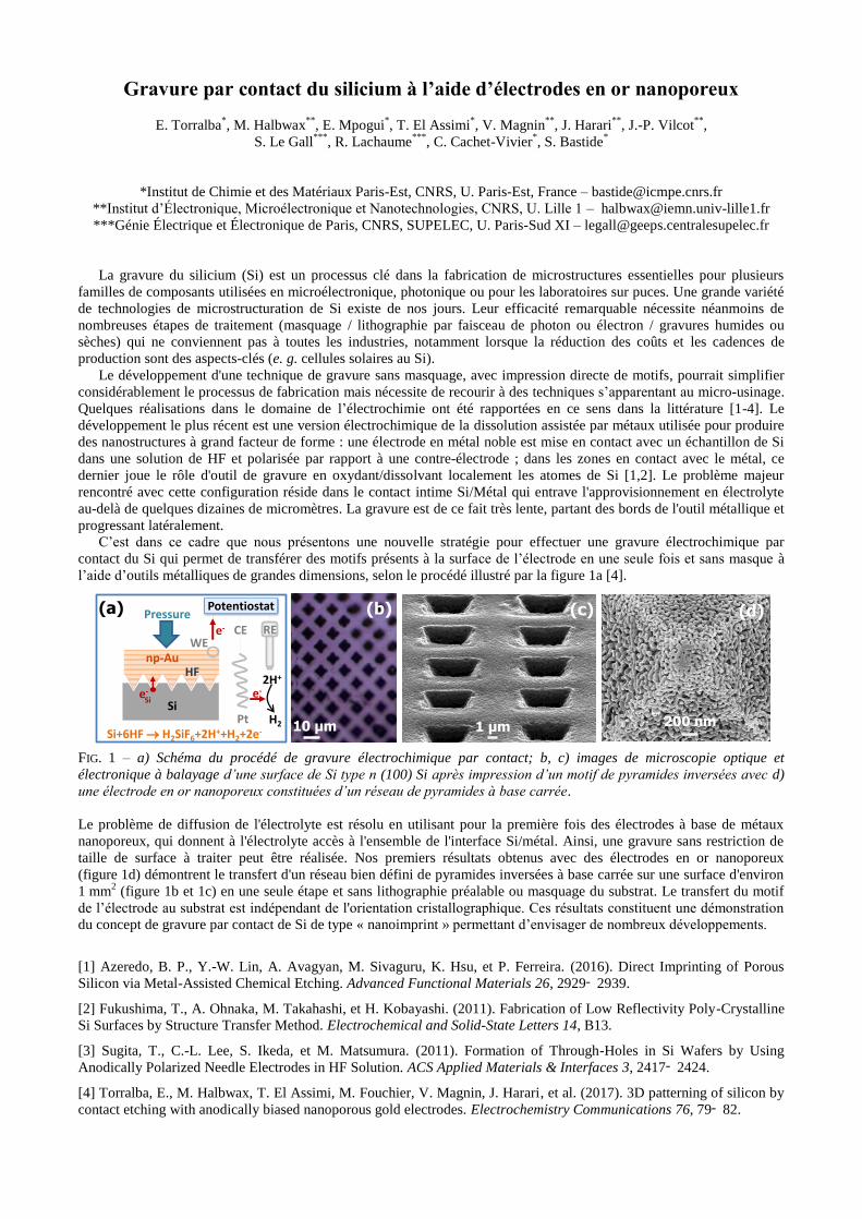
l’aide d’outils métalliques de grandes dimensions, selon le procédé illustré par la figure 1a [4].
FIG. 1 – a) Schéma du procédé de gravure électrochimique par contact; b, c) images de microscopie optique et
électronique à balayage d’une surface de Si type n (100) Si après impression d’un motif de pyramides inversées avec d)
une électrode en or nanoporeux constituées d’un réseau de pyramides à base carrée.
Le problème de diffusion de l'électrolyte est résolu en utilisant pour la première fois des électrodes à base de métaux
nanoporeux, qui donnent à l'électrolyte accès à l'ensemble de l'interface Si/métal. Ainsi, une gravure sans restriction de
taille de surface à traiter peut être réalisée. Nos premiers résultats obtenus avec des électrodes en or nanoporeux
(figure 1d) démontrent le transfert d'un réseau bien défini de pyramides inversées à base carrée sur une surface d'environ
1 mm2 (figure 1b et 1c) en une seule étape et sans lithographie préalable ou masquage du substrat. Le transfert du motif
de l’électrode au substrat est indépendant de l'orientation cristallographique. Ces résultats constituent une démonstration
du concept de gravure par contact de Si de type « nanoimprint » permettant d’envisager de nombreux développements.
[1] Azeredo, B. P., Y.-W. Lin, A. Avagyan, M. Sivaguru, K. Hsu, et P. Ferreira. (2016). Direct Imprinting of Porous
Silicon via Metal-Assisted Chemical Etching. Advanced Functional Materials 26, 2929‑ 2939.
[2] Fukushima, T., A. Ohnaka, M. Takahashi, et H. Kobayashi. (2011). Fabrication of Low Reflectivity Poly-Crystalline
Si Surfaces by Structure Transfer Method. Electrochemical and Solid-State Letters 14, B13.
[3] Sugita, T., C.-L. Lee, S. Ikeda, et M. Matsumura. (2011). Formation of Through-Holes in Si Wafers by Using
Anodically Polarized Needle Electrodes in HF Solution. ACS Applied Materials & Interfaces 3, 2417‑ 2424.
[4] Torralba, E., M. Halbwax, T. El Assimi, M. Fouchier, V. Magnin, J. Harari, et al. (2017). 3D patterning of silicon by
contact etching with anodically biased nanoporous gold electrodes. Electrochemistry Communications 76, 79‑ 82.
1 µm
(c)
Si
2H+
H2
e-
Pt
e-
e-
Si+6HF H2SiF6+2H++H2+2e-
RE
Potentiostat
CEWE
Si
HFnp-Au
(a) Pressure (b)
10 µm
(d)
200 nm
Surfaces nanostructurées imprégnées et applications.
Sawsen Zouaghi, Abderrahmane Hamdi, Maude Jimenez, Thomas Dargent, Yannick Coffinier & Vincent Thomy
Institut d’Electronique, de Microélectronique et de Nanotechnologie (IEMN, UMR CNRS 8520), Université Lille1, Cite Scientifique, Avenue Poincaré, BP 60069, 59652 Villeneuve d’Ascq, France. email : [email protected] Alors que les surfaces superhydrophobes ont connu un très fort engouement au début des années 2000, il s’est
très vite posé le problème de leur réelle utilisation : limitées à des liquides aqueux, les applications possibles s’en
sont trouvées très restreintes. En 2007, les travaux pionniers du groupe de McKinley et Cohen du MIT, sur le
développement de surfaces dites superoléophobes, ont permis d’étendre la gamme de liquides étudiés [1]. Ces
surfaces présentent un non mouillage (maintien d’un état de Cassie-Baxter grâce à l'emprisonnement des poches
d’air sous le liquide) y compris pour des liquides à faible tension de surface (liquides non polaires, alcools,
huiles, …). Contrairement aux surfaces superhydrophobes, la conception de surfaces oléophobes est plus
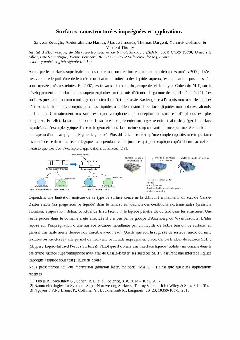
complexe. En effet, la structuration de la surface doit présenter un angle ré-entrant afin de piéger l’interface
liquide/air. L’exemple typique d’une telle géométrie est la structure surplombante formée par une tête de clou ou
le chapeau d’un champignon (Figure de gauche). Plus difficile à réaliser qu’une simple rugosité, une importante
diversité de réalisations technologiques a cependant vu le jour ce qui peut expliquer qu'à l'heure actuelle il
n'existe que très peu d'exemple d'applications concrètes [2,3].
Cependant une limitation majeure de ce type de surface concerne la difficulté à maintenir un état de Cassie-
Baxter stable (air piégé sous le liquide) dans le temps : en fonction des conditions expérimentales (pression,
vibration, évaporation, défaut ponctuel de la surface, …) le liquide pénètre tôt ou tard dans les structures. Une
réelle percée dans le domaine a été effectuée il y a peu par le groupe d’Aizenberg du Wyss Institute. L’idée
repose sur l’imprégnation d’une surface texturée mouillante par un liquide de faible tension de surface (en
général une huile inerte fluorée non miscible avec l’eau). Quelle que soit la rugosité de surface (micro ou nano
texturée ou structurée), elle permet de maintenir le liquide imprégné en place. On parle alors de surface SLIPS
(Slippery Liquid-Infused Porous Surfaces). Plutôt que d’obtenir une interface liquide / solide / air comme dans le
cas d’une surface superomniphobe avec état de Cassie-Baxter, les surfaces SLIPS assurent une interface liquide
imprégné / liquide sous test (Figure de droite).
Nous présenterons ici leur fabrication (ablation laser, méthode "MACE"...) ainsi que quelques applications
récentes.
[1] Tuteja A., McKinley G., Cohen, R. E. et al., Science, 318, 1618 – 1622, 2007 [2] Nanotechnologies for Synthetic Super Non-wetting Surfaces, Thomy V. et al. John Wiley & Sons Ed., 2014 [3] Nguyen T.P.N., Brunet P., Coffinier Y., Boukherroub R., Langmuir, 26, 23, 18369-18373, 2010
Fabrication of Lateral Porous Silicon Membranes by Means of Ion Implantation
Yingning He*, Douglas Silva De Vasconcellos*, Eric Imbernon*, David Bourrier*, Thierry Leichle*
*CNRS, LAAS, 7 avenue du colonel Roche, F-31400 Toulouse, France – [email protected]
In this work, we present a fabrication process (Fig. 1) for the realization of lateral porous silicon membranes with
tunable pore size and porosity (Fig. 2) and their integration into planar microfluidics. Since the formation of porous
silicon by anodization is highly dependent on the dopant type and concentration [1], we use ion implantation to
manipulate the local dopant concentration in order to control the membrane properties. The dead-end filtration capability
[2] of fabricated lateral porous silicon membranes is demonstrated by adequately retaining 300 nm diameter beads, while
small biomolecules permeate the membranes (Fig. 3). Finally, since the inner pore surface is negatively charged in
physiological buffer, the membranes exhibit ion depletion phenomena upon electric field application, which indicates
that they can act as cation perm-selective membranes [3] for molecule separation (Fig. 4).
FIG. 1 – Fabrication process of lateral porous silicon
membranes using ion implantation. (a) Boron and (b)
Phosphorus implantation. (c) Dry etching to create
microchannels. (d) Patterning of the working electrode.
(e) Silicon anodization. (f) Fabrication of inlets/outlets
by sandblasting and channel sealing by anodic bonding.
FIG. 3 – Filtering capability of the fabricated lateral
porous silicon membrane tested by flowing fluorescein,
miRNA, and 300 nm diameter beads. The white arrows
indicate the direction of the fluid flow. The porous
silicon membrane is located in the center of each
image. The biomolecules can flow back and forth
through the membrane while beads are prevented from
passing through the membrane.
FIG. 2 – (a) Optical photograph of a fabricated fluidic
chip integrating a porous silicon membrane. (b) SEM
picture of the porous membrane bridging two channels.
(c) SEM close-up of the membrane showing the
protective top n-type layer. Variation of membrane
porosity (d) and pore size (e) with the current density
used during silicon anodization.
FIG. 4 – Ion depletion phenomena happening at the
microchannel/porous membrane interface. (a) Layout of
the device: the top microchannel is filled with a mixture
of fluorescein; the bottom microchannel is filled with
buffer; Pt electrodes are inserted in the reservoirs; 10 V
is applied across the porous membrane. (b) and (c): the
negatively charged porous membrane only allows
cations to pass through, which leads to an ion depletion
region in the vicinity of the porous membrane.
[1] Eijkel, C. J. M., Branebjerg, J., Elwenspoek, M., & Van de Pol, F. C. M. (1990). Electron Device Letters,
IEEE, 11(12), 588-589.
[2] Leïchlé, T., & Bourrier, D. (2015). Lab on a Chip, 15(3), 833-838.
[3] Kim, S. J., Wang, Y. C., Lee, J. H., Jang, H., & Han, J. (2007). Physical review letters, 99(4), 044501.
Fabrication de membranes en silicium poreux et exemples d’applications
Sébastien DESPLOBAIN*, Laurent VENTURA*,**
Benjamin BARDET**, Thomas DEFFORGE**, Gaël GAUTIER**, Jérome Billoué**
*SiLiMiXT c/o STMicroelectronics 10 rue Thalès de Milet, 37071, Tours – [email protected]
** CNRS-GREMAN UMR 7347, c/o STMicroelectronics 10 rue Thalès de Milet, 37071, Tours
SiLiMiXT-SAS est une start-up issue des travaux de recherche du laboratoire CNRS-GREMAN UMR 7347. Créée en
2013, SiLiMiXT a l’objectif de produire des structures en silicium poreux et de développer des solutions industrialisables
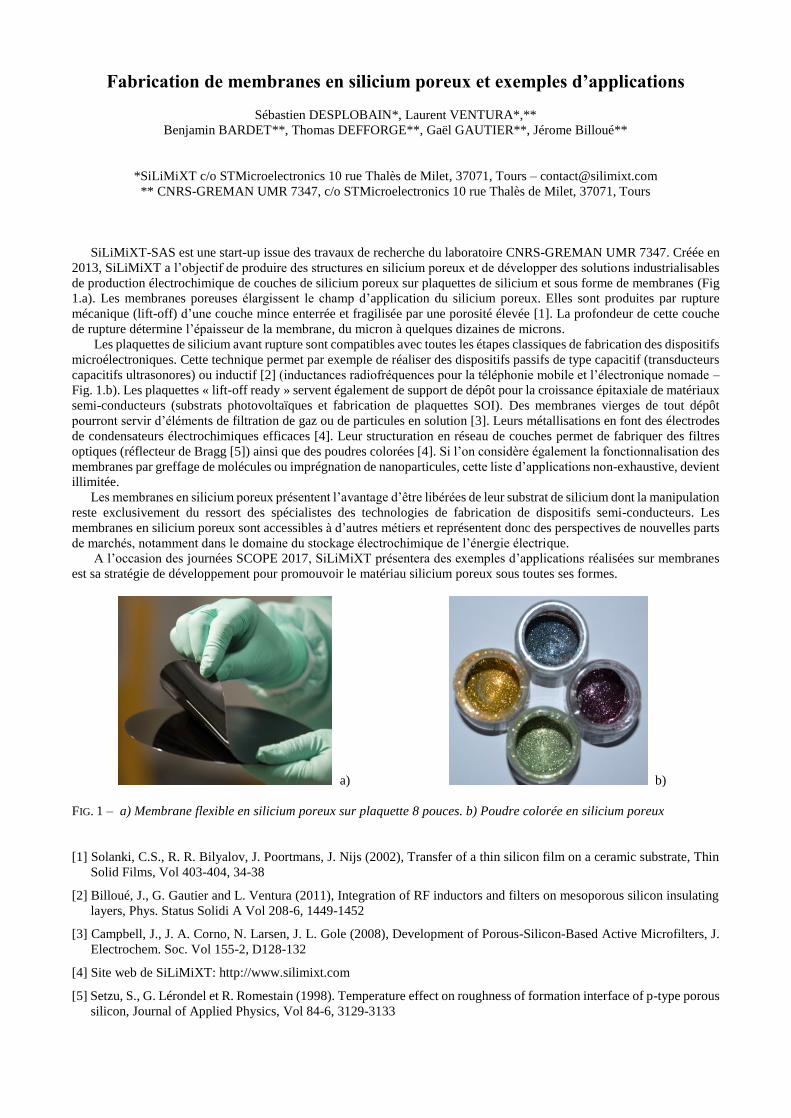
de production électrochimique de couches de silicium poreux sur plaquettes de silicium et sous forme de membranes (Fig
1.a). Les membranes poreuses élargissent le champ d’application du silicium poreux. Elles sont produites par rupture
mécanique (lift-off) d’une couche mince enterrée et fragilisée par une porosité élevée [1]. La profondeur de cette couche
de rupture détermine l’épaisseur de la membrane, du micron à quelques dizaines de microns.
Les plaquettes de silicium avant rupture sont compatibles avec toutes les étapes classiques de fabrication des dispositifs
microélectroniques. Cette technique permet par exemple de réaliser des dispositifs passifs de type capacitif (transducteurs
capacitifs ultrasonores) ou inductif [2] (inductances radiofréquences pour la téléphonie mobile et l’électronique nomade –
Fig. 1.b). Les plaquettes « lift-off ready » servent également de support de dépôt pour la croissance épitaxiale de matériaux
semi-conducteurs (substrats photovoltaïques et fabrication de plaquettes SOI). Des membranes vierges de tout dépôt
pourront servir d’éléments de filtration de gaz ou de particules en solution [3]. Leurs métallisations en font des électrodes
de condensateurs électrochimiques efficaces [4]. Leur structuration en réseau de couches permet de fabriquer des filtres
optiques (réflecteur de Bragg [5]) ainsi que des poudres colorées [4]. Si l’on considère également la fonctionnalisation des
membranes par greffage de molécules ou imprégnation de nanoparticules, cette liste d’applications non-exhaustive, devient
illimitée.
Les membranes en silicium poreux présentent l’avantage d’être libérées de leur substrat de silicium dont la manipulation
reste exclusivement du ressort des spécialistes des technologies de fabrication de dispositifs semi-conducteurs. Les
membranes en silicium poreux sont accessibles à d’autres métiers et représentent donc des perspectives de nouvelles parts
de marchés, notamment dans le domaine du stockage électrochimique de l’énergie électrique.
A l’occasion des journées SCOPE 2017, SiLiMiXT présentera des exemples d’applications réalisées sur membranes
est sa stratégie de développement pour promouvoir le matériau silicium poreux sous toutes ses formes.
a) b)
FIG. 1 – a) Membrane flexible en silicium poreux sur plaquette 8 pouces. b) Poudre colorée en silicium poreux
[1] Solanki, C.S., R. R. Bilyalov, J. Poortmans, J. Nijs (2002), Transfer of a thin silicon film on a ceramic substrate, Thin
Solid Films, Vol 403-404, 34-38
[2] Billoué, J., G. Gautier and L. Ventura (2011), Integration of RF inductors and filters on mesoporous silicon insulating
layers, Phys. Status Solidi A Vol 208-6, 1449-1452
[3] Campbell, J., J. A. Corno, N. Larsen, J. L. Gole (2008), Development of Porous-Silicon-Based Active Microfilters, J.
Electrochem. Soc. Vol 155-2, D128-132
[4] Site web de SiLiMiXT: http://www.silimixt.com
[5] Setzu, S., G. Lérondel et R. Romestain (1998). Temperature effect on roughness of formation interface of p-type porous
silicon, Journal of Applied Physics, Vol 84-6, 3129-3133
Stabilization of porous silicon in aqueous buffer using atomic layer deposited
hafnium oxide
Jonathan Rasson, Laurent A. Francis
Institute of Information and Communication Technologies, Electronics and Applied Mathematics (ICTEAM),
Université catholique de Louvain, Place du Levant 3, 1348 Louvain-la-Neuve, Belgique
As porous silicon (PSi) is widely used for sensing and biosensing applications, it is often exposed to aqueous media.
Unfortunately, PSi is unstable in presence of water due to the oxidation/dissolution of the Si scaffold, which leads to
significant shifts in its optical properties and thus prevents an accurate reading of measurements for a sensitive detection
[1]. Several methods modifying the PSi chemistry have been successfully applied to solve this issue, such as the
carbonization [2], hydrosylilation [2] and ozone oxidation [3] with the most used being the thermal oxidation [1].
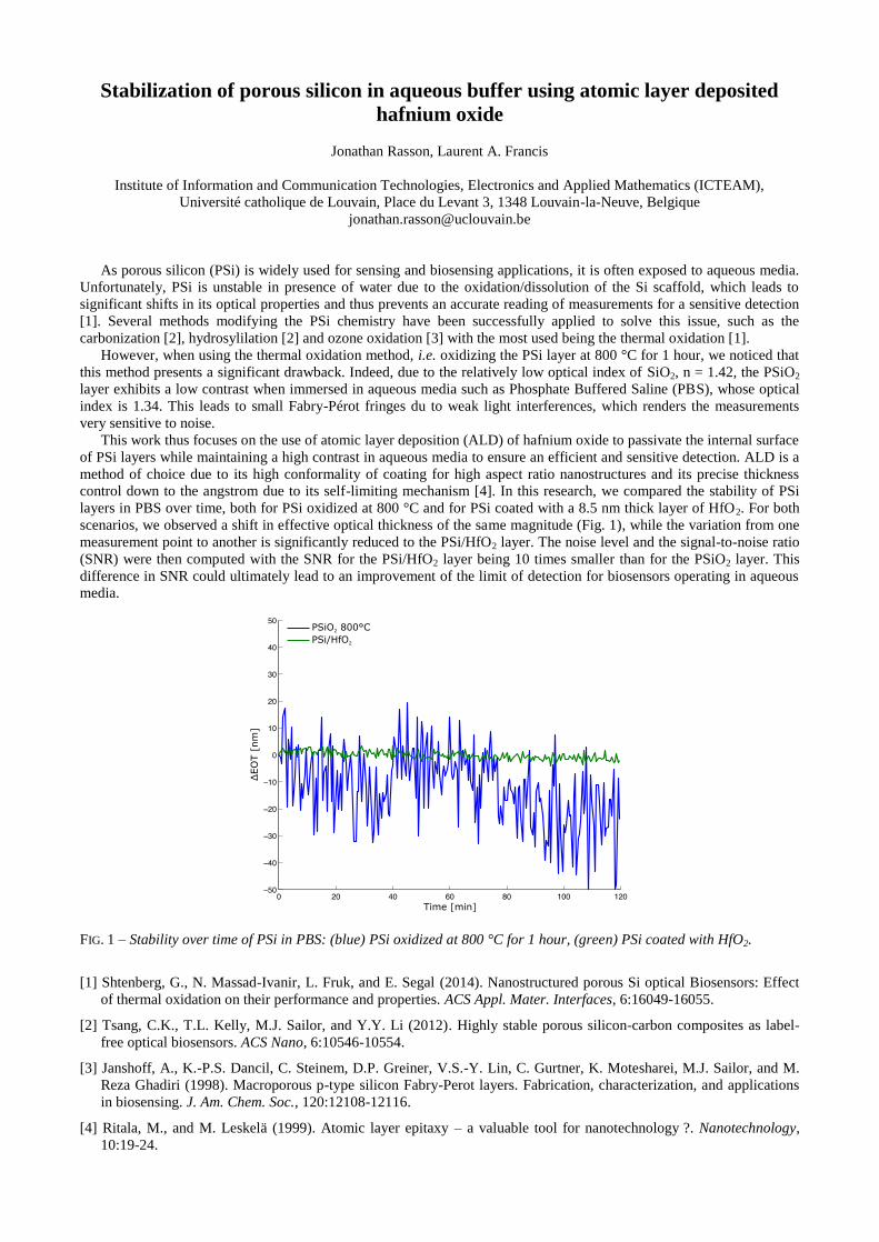
However, when using the thermal oxidation method, i.e. oxidizing the PSi layer at 800 °C for 1 hour, we noticed that
this method presents a significant drawback. Indeed, due to the relatively low optical index of SiO2, n = 1.42, the PSiO2
layer exhibits a low contrast when immersed in aqueous media such as Phosphate Buffered Saline (PBS), whose optical
index is 1.34. This leads to small Fabry-Pérot fringes du to weak light interferences, which renders the measurements
very sensitive to noise.
This work thus focuses on the use of atomic layer deposition (ALD) of hafnium oxide to passivate the internal surface
of PSi layers while maintaining a high contrast in aqueous media to ensure an efficient and sensitive detection. ALD is a
method of choice due to its high conformality of coating for high aspect ratio nanostructures and its precise thickness
control down to the angstrom due to its self-limiting mechanism [4]. In this research, we compared the stability of PSi
layers in PBS over time, both for PSi oxidized at 800 °C and for PSi coated with a 8.5 nm thick layer of HfO2. For both
scenarios, we observed a shift in effective optical thickness of the same magnitude (Fig. 1), while the variation from one
measurement point to another is significantly reduced to the PSi/HfO2 layer. The noise level and the signal-to-noise ratio
(SNR) were then computed with the SNR for the PSi/HfO2 layer being 10 times smaller than for the PSiO2 layer. This
difference in SNR could ultimately lead to an improvement of the limit of detection for biosensors operating in aqueous
media.
FIG. 1 – Stability over time of PSi in PBS: (blue) PSi oxidized at 800 °C for 1 hour, (green) PSi coated with HfO2.
[1] Shtenberg, G., N. Massad-Ivanir, L. Fruk, and E. Segal (2014). Nanostructured porous Si optical Biosensors: Effect
of thermal oxidation on their performance and properties. ACS Appl. Mater. Interfaces, 6:16049-16055.
[2] Tsang, C.K., T.L. Kelly, M.J. Sailor, and Y.Y. Li (2012). Highly stable porous silicon-carbon composites as label-
free optical biosensors. ACS Nano, 6:10546-10554.
[3] Janshoff, A., K.-P.S. Dancil, C. Steinem, D.P. Greiner, V.S.-Y. Lin, C. Gurtner, K. Motesharei, M.J. Sailor, and M.
Reza Ghadiri (1998). Macroporous p-type silicon Fabry-Perot layers. Fabrication, characterization, and applications
in biosensing. J. Am. Chem. Soc., 120:12108-12116.
[4] Ritala, M., and M. Leskelä (1999). Atomic layer epitaxy – a valuable tool for nanotechnology ?. Nanotechnology,
10:19-24.
Fabrication of porous silicon layer on silicon-on-insulator surface and its use for
laser desorption/ionization of peptides and antibiotics and their detection by mass
spectrometry.
Abderrahmane Hamdi, Rabah Boukherroub & Yannick Coffinier
Institut d’Electronique, de Microélectronique et de Nanotechnologie (IEMN, UMR CNRS 8520), Université Lille1, Cite
Scientifique, Avenue Poincaré, BP 60069, 59652 Villeneuve d’Ascq, France.
email : [email protected]
Résumé : Matrix-assisted laser desorption/ionization mass spectrometry (MALDI-MS) has become a widespread analytical tool for
peptides, proteins, metabolites and other biomolecules. However, due to a competitive desorption of parasitic ions from
the matrix, it is difficult to detect low molecular weight compounds (<700 Da). To enable desorption/ionization of small
molecules, techniques operating in absence of an organic matrix were developed. These techniques known as surface-
assisted laser desorption/ionization mass spectrometry (SALDI-MS) rely on the use of nanostructured surfaces as laser
desorption/ionization-assisted material. As compared to traditional MALDI-MS, SALDI-MS offers several advantages
such as the ability to detect small molecules (< 500 Da), easy sample preparation, low noise background, high salt
tolerance and fast data collection.1 Many types of micro-nanostructured surfaces have already been designed and
prepared keeping particular attention to surface morphologies and chemical functionalizations.2 It was reported that pore
size and depth, nanostructure sizes, surface porosity, and roughness could affect LDI efficiencies. For instance, the length
of nanostructured layers plays several roles.3 First, the length should be high enough to correctly absorb photons from
pulsed laser irradiation. Indeed, the laser penetration depth in the silicon nanostructures at the wavelength of 355 nm is
lower than 100 nm, considering the nanostructure optical absorption and reflection in this energy range. Second, analytes
have to be correctly and uniformly distributed inside the nanostructured layer to be efficiently desorbed and ionized.
However, when the thickness of the layer is too high, analytes could also be trapped deeply inside the nanostructured
layer. Then, although the energy was appropriately transferred to analytes, the desorption stage (plume formation and
expansion) could be less efficient and thus led to a decrease of the detection sensitivity.
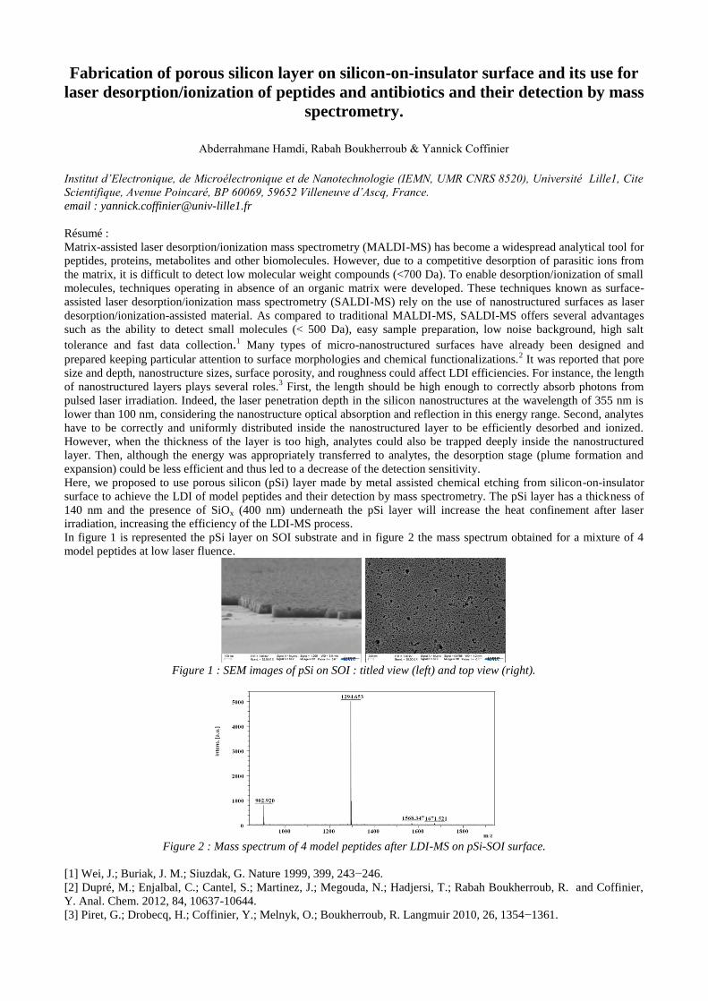
Here, we proposed to use porous silicon (pSi) layer made by metal assisted chemical etching from silicon-on-insulator
surface to achieve the LDI of model peptides and their detection by mass spectrometry. The pSi layer has a thickness of
140 nm and the presence of SiOx (400 nm) underneath the pSi layer will increase the heat confinement after laser
irradiation, increasing the efficiency of the LDI-MS process.
In figure 1 is represented the pSi layer on SOI substrate and in figure 2 the mass spectrum obtained for a mixture of 4
model peptides at low laser fluence.
Figure 1 : SEM images of pSi on SOI : titled view (left) and top view (right).
Figure 2 : Mass spectrum of 4 model peptides after LDI-MS on pSi-SOI surface.
[1] Wei, J.; Buriak, J. M.; Siuzdak, G. Nature 1999, 399, 243−246.
[2] Dupré, M.; Enjalbal, C.; Cantel, S.; Martinez, J.; Megouda, N.; Hadjersi, T.; Rabah Boukherroub, R. and Coffinier,
Y. Anal. Chem. 2012, 84, 10637-10644.
[3] Piret, G.; Drobecq, H.; Coffinier, Y.; Melnyk, O.; Boukherroub, R. Langmuir 2010, 26, 1354−1361.
Optimisation de la photoluminescence de particules de silicium
microporeux
Thomas Defforge, Gaël Gautier
Université François Rabelais de Tours, CNRS, CEA, INSA-CVL, GREMAN UMR 7347, Tours, France
Le suivi in situ de la dégradation des nanoparticules de silicium poreux fait partie des principales
applications actuelles de ce matériau dans le domaine biomédical, notamment pour la libération de principes
actifs piégés dans la matrice poreuse [1]. Pour ce faire, les propriétés photoluminescentes (PL) des particules
poreuses sont généralement utilisées [1,2]. Ce résumé reprend les différentes études qui ont été menées ces
dernières années au GREMAN en partenariat avec plusieurs laboratoires étrangers afin d’étudier la morphologie
des particules poreuses obtenues par gravure électrochimique et d’en optimiser les propriétés PL.
La gravure électrochimique dans un électrolyte à base d’acide fluorhydrique mélangé à un acide fort (acide
chlorhydrique ou sulfurique concentré) de substrats de type p faiblement dopés a permis la formation d’une
couche de silicium micro/mésoporeuse (les dimensions des pores variant de 2 à 4 nm) à très forte surface
spécifique (> 800m²/g) [3]. L’ajout d’un acide fort à l’électrolyte présente l’avantage de limiter la gravure
chimique du silicium au cours des étapes de formation et de rinçage du silicium poreux. Les propriétés PL de ces
structures ont alors été analysées et le rendement quantique a été calculé [4]. Pour améliorer le rendement
quantique, les particules – habituellement séchées à l’air après rinçage – ont été séchées au sécheur supercritique
afin de conserver la nanostructure poreuse intacte [5]. L’apport du séchage supercritique a été spéctaculaire dans
l’augmentation du rendement quantique de PL des particules poreuses (passant de 17.5% à 32.1%). Enfin, la
chimie de surface de ces mêmes particules microporeuses a récemment été modifiée par hydrosilylation en
présence d’acide undecylénique et l’intensité de PL a été mesurée. Cette dernière a été doublée après
fonctionnalisation des particules. Le rendement quantique des particules fonctionnalisées est actuellement au
cours d’investigation auprès de nos partenaires.
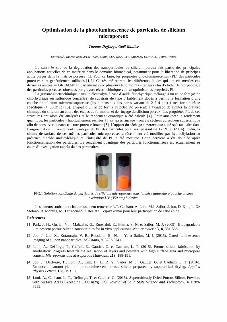
FIG.1 Solution colloïdale de particules de silicium microporeux sous lumière naturelle à gauche et sous
excitation UV (350 nm) à droite.
Les auteurs souhaitent chaleureusement remercier L.T. Canham, A. Loni, M.J. Sailor, J. Joo, D. Kim, L. De
Stefano, R. Moretta, M. Terracciano, I. Rea et S. Vijayakumar pour leur participation de cette étude.
References
[1] Park, J. H., Gu, L., Von Maltzahn, G., Ruoslahti, E., Bhatia, S. N. et Sailor, M. J. (2009). Biodegradable
luminescent porous silicon nanoparticles for in vivo applications. Nature materials, 8, 331-336.
[2] Joo, J., Liu, X., Kotamraju, V. R., Ruoslahti, E., Nam, Y. et Sailor, M. J. (2015). Gated luminescence
imaging of silicon nanoparticles. ACS nano, 9, 6233-6241.
[3] Loni, A., Defforge, T., Caffull, E., Gautier, G. et Canham, L. T. (2015). Porous silicon fabrication by
anodisation: Progress towards the realisation of layers and powders with high surface area and micropore
content. Microporous and Mesoporous Materials, 213, 188-191.
[4] Joo, J., Defforge, T., Loni, A., Kim, D., Li, Z. Y., Sailor, M. J., Gautier, G. et Canham, L. T. (2016).
Enhanced quantum yield of photoluminescent porous silicon prepared by supercritical drying. Applied
Physics Letters, 108, 153111.
[5] Loni, A., Canham, L. T., Defforge, T. et Gautier, G. (2015). Supercritically-Dried Porous Silicon Powders
with Surface Areas Exceeding 1000 m2/g. ECS Journal of Solid State Science and Technology, 4, P289-
P292.
Manufacture and development of all-solid-state Li-ion micro battery based on nanostructured materials
Yasemin Duygu YUCEL*, Thierry DJENIZIAN**
*MADIREL Laboratoire, Aix Marseille Université-CNRS UMR7246, Centre de St-Jérome, F-13397 Marseille cedex 20-
[email protected] **Flexible Electronics Department, Ecole National Supérieure des Mines, Gardanne 13 541, France-
We report on the fabrication of all-solid state Li-ion micro battery (µLIB) to replace a primary battery currently being used to power an intelligent device developed by a microelectronic company. This microbattery is consisted of a nano-architected anode (TiO2 nanotubes self-organized), a polymer electrolyte in a manner consistent electrodeposited on the tube walls and a high potential cathode.
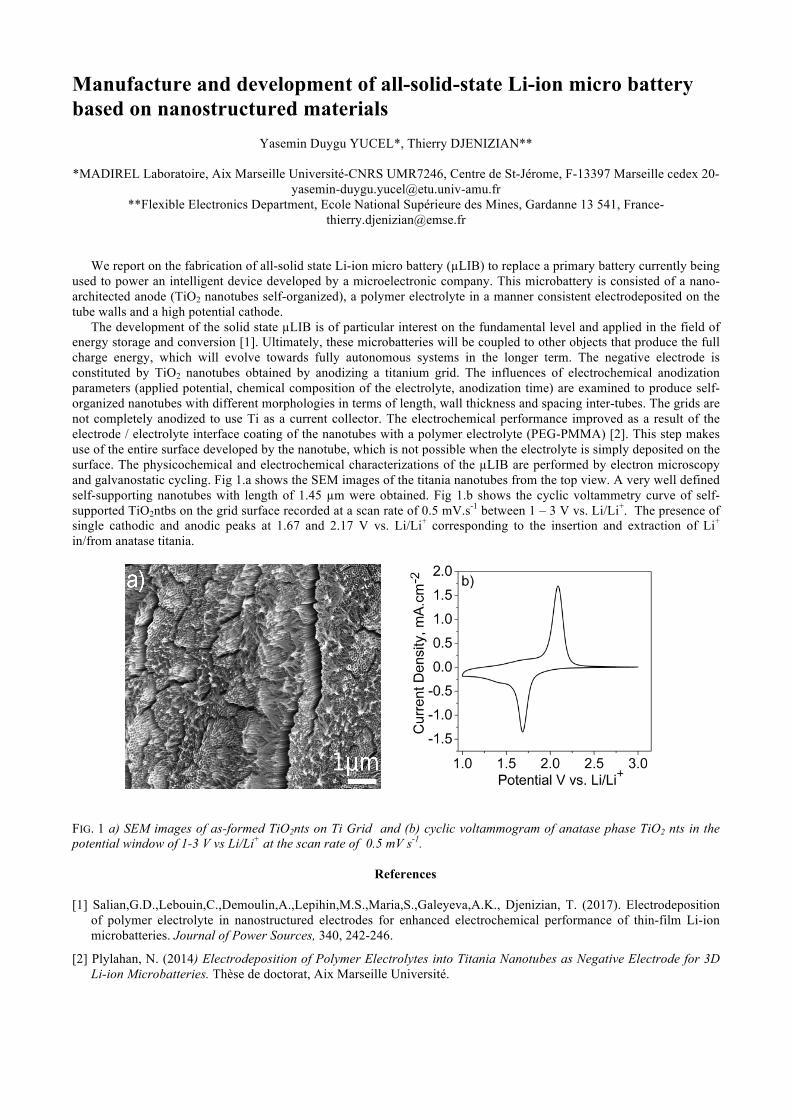
The development of the solid state µLIB is of particular interest on the fundamental level and applied in the field of energy storage and conversion [1]. Ultimately, these microbatteries will be coupled to other objects that produce the full charge energy, which will evolve towards fully autonomous systems in the longer term. The negative electrode is constituted by TiO2 nanotubes obtained by anodizing a titanium grid. The influences of electrochemical anodization parameters (applied potential, chemical composition of the electrolyte, anodization time) are examined to produce self-organized nanotubes with different morphologies in terms of length, wall thickness and spacing inter-tubes. The grids are not completely anodized to use Ti as a current collector. The electrochemical performance improved as a result of the electrode / electrolyte interface coating of the nanotubes with a polymer electrolyte (PEG-PMMA) [2]. This step makes use of the entire surface developed by the nanotube, which is not possible when the electrolyte is simply deposited on the surface. The physicochemical and electrochemical characterizations of the µLIB are performed by electron microscopy and galvanostatic cycling. Fig 1.a shows the SEM images of the titania nanotubes from the top view. A very well defined self-supporting nanotubes with length of 1.45 µm were obtained. Fig 1.b shows the cyclic voltammetry curve of self-supported TiO2ntbs on the grid surface recorded at a scan rate of 0.5 mV.s-1 between 1 – 3 V vs. Li/Li+. The presence of single cathodic and anodic peaks at 1.67 and 2.17 V vs. Li/Li+ corresponding to the insertion and extraction of Li+ in/from anatase titania.
FIG. 1 a) SEM images of as-formed TiO2nts on Ti Grid and (b) cyclic voltammogram of anatase phase TiO2 nts in the potential window of 1-3 V vs Li/Li+ at the scan rate of 0.5 mV s-1.
References
[1] Salian,G.D.,Lebouin,C.,Demoulin,A.,Lepihin,M.S.,Maria,S.,Galeyeva,A.K., Djenizian, T. (2017). Electrodeposition of polymer electrolyte in nanostructured electrodes for enhanced electrochemical performance of thin-film Li-ion microbatteries. Journal of Power Sources, 340, 242-246.
[2] Plylahan, N. (2014) Electrodeposition of Polymer Electrolytes into Titania Nanotubes as Negative Electrode for 3D Li-ion Microbatteries. Thèse de doctorat, Aix Marseille Université.
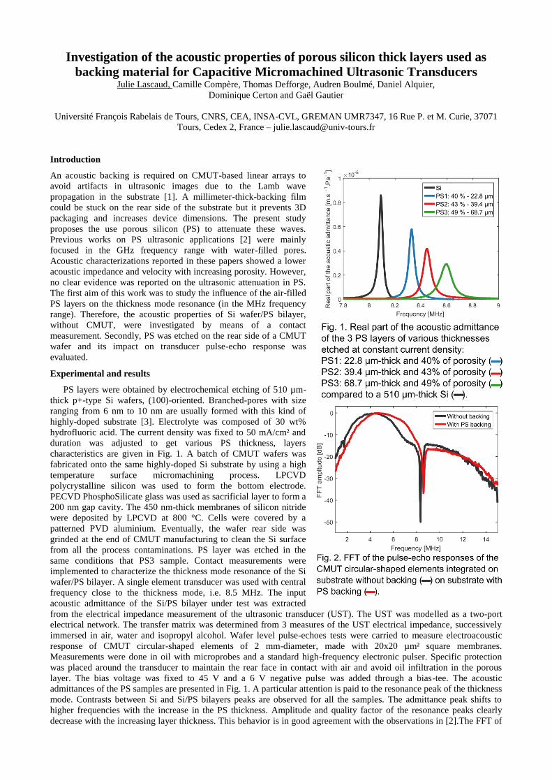
Investigation of the acoustic properties of porous silicon thick layers used as
backing material for Capacitive Micromachined Ultrasonic Transducers
Julie Lascaud, Camille Compère, Thomas Defforge, Audren Boulmé, Daniel Alquier,
Dominique Certon and Gaël Gautier
Université François Rabelais de Tours, CNRS, CEA, INSA-CVL, GREMAN UMR7347, 16 Rue P. et M. Curie, 37071
Tours, Cedex 2, France – [email protected]
Introduction
An acoustic backing is required on CMUT-based linear arrays to
avoid artifacts in ultrasonic images due to the Lamb wave
propagation in the substrate [1]. A millimeter-thick-backing film
could be stuck on the rear side of the substrate but it prevents 3D
packaging and increases device dimensions. The present study
proposes the use porous silicon (PS) to attenuate these waves.
Previous works on PS ultrasonic applications [2] were mainly
focused in the GHz frequency range with water-filled pores.
Acoustic characterizations reported in these papers showed a lower
acoustic impedance and velocity with increasing porosity. However,
no clear evidence was reported on the ultrasonic attenuation in PS.
The first aim of this work was to study the influence of the air-filled
PS layers on the thickness mode resonance (in the MHz frequency
range). Therefore, the acoustic properties of Si wafer/PS bilayer,
without CMUT, were investigated by means of a contact
measurement. Secondly, PS was etched on the rear side of a CMUT
wafer and its impact on transducer pulse-echo response was
evaluated.
Experimental and results
PS layers were obtained by electrochemical etching of 510 µm-
thick p+-type Si wafers, (100)-oriented. Branched-pores with size
ranging from 6 nm to 10 nm are usually formed with this kind of
highly-doped substrate [3]. Electrolyte was composed of 30 wt%
hydrofluoric acid. The current density was fixed to 50 mA/cm² and
duration was adjusted to get various PS thickness, layers
characteristics are given in Fig. 1. A batch of CMUT wafers was
fabricated onto the same highly-doped Si substrate by using a high
temperature surface micromachining process. LPCVD
polycrystalline silicon was used to form the bottom electrode.
PECVD PhosphoSilicate glass was used as sacrificial layer to form a
200 nm gap cavity. The 450 nm-thick membranes of silicon nitride
were deposited by LPCVD at 800 °C. Cells were covered by a
patterned PVD aluminium. Eventually, the wafer rear side was
grinded at the end of CMUT manufacturing to clean the Si surface
from all the process contaminations. PS layer was etched in the
same conditions that PS3 sample. Contact measurements were
implemented to characterize the thickness mode resonance of the Si
wafer/PS bilayer. A single element transducer was used with central
frequency close to the thickness mode, i.e. 8.5 MHz. The input
acoustic admittance of the Si/PS bilayer under test was extracted
from the electrical impedance measurement of the ultrasonic transducer (UST). The UST was modelled as a two-port
electrical network. The transfer matrix was determined from 3 measures of the UST electrical impedance, successively
immersed in air, water and isopropyl alcohol. Wafer level pulse-echoes tests were carried to measure electroacoustic
response of CMUT circular-shaped elements of 2 mm-diameter, made with 20x20 µm² square membranes.
Measurements were done in oil with microprobes and a standard high-frequency electronic pulser. Specific protection
was placed around the transducer to maintain the rear face in contact with air and avoid oil infiltration in the porous
layer. The bias voltage was fixed to 45 V and a 6 V negative pulse was added through a bias-tee. The acoustic
admittances of the PS samples are presented in Fig. 1. A particular attention is paid to the resonance peak of the thickness
mode. Contrasts between Si and Si/PS bilayers peaks are observed for all the samples. The admittance peak shifts to
higher frequencies with the increase in the PS thickness. Amplitude and quality factor of the resonance peaks clearly
decrease with the increasing layer thickness. This behavior is in good agreement with the observations in [2].The FFT of
Titre court de votre article en 10 mots maximum
the pulse-echo responses of the CMUT circular-shaped elements with and without PS backing are shown in Fig. 2.
A cutoff imputed to thickness mode resonance is observed on the spectrum of the element integrated on the Si. The notch
amplitude varies from -35 dB, without backing, to -20 dB with PS backing. As for impedance measurement, substrate
ringing frequency is increased of 0.3 MHz.
Conclusion
The acoustic properties of PS layers were investigated in order to use it as backing for CMUT. The influence of PS on
the pulse-echo response of circular-shaped CMUT elements was estimated. Frequency responses of both transducers with
and without backing show that PS substantially reduces the cutoff due to thickness mode resonance. Further
measurements along elements of an array are currently being performed to quantify Lamb wave attenuation efficiency.
Acknowledgment
This work has been funded by the “Région Centre” in the frame of the SIPeMUT research project (2013-00083160). The
authors would like to thank the Conseil Departemental d’Indre et Loire for their financial supports.
References
[1] Oralkan, et al., Ultrasonics, IEEE Transactions on Ferroelectrics, and Frequency Control, 49 (2002), 1596-1610
[2] Aliev, G. N., et al., Journal of Applied Physics, 110 (2011), 043534
[3] Capelle, M., et al., IEEE Transactions on Electron Devices, 62(2015), 4169-417 [3] Lioni, A., C. Sauwens, G.
Theraulaz, et J.L. Deneubourg (2001)., 14:679-696.
Porous Silicon Nanoparticles for Cancer Theragnostic
Cueto Diaz, Eduardo *; Chaix, Arnaud*; Pichon, Chantal **; Midoux, Patrick ** Gary-Bobo, Magali ***; Maynadier,
Marie ***, Morère, Alain ***; Garcia, Marcel ***; Durand, Jean-Olivier*; Cunin, Frederique*
*Institut Charles Gerhardt Montpellier, Université de Montpellier Bât.17 (UMR5253)
** Centre de Biophysique Moléculaire in Orleans (CBM, UPR4301)
*** Centre des Biomolécules Max Mousseron (IBMM, UMR5247)
[email protected], [email protected]
During the last years, the oncology research has focused its attention in the development of nanomaterials (NMs)
bearing both diagnostic and cancer-treatment properties. In that sense, is of great value, that the nanomaterial displays
certain grade of stealthiness, during a reasonable period so that its diagnostic or therapeutic function can be carried out
before clearance. Along with the previous properties, NMs must also exhibit some sort of biocompatibility and
biodegradability, a crucial factor in biological environments. Porous silicon nanoparticles (pSiNps) have emerged as a
promising and versatile platform for nanomedicine. Their outstanding properties, including excellent in vivo
biocompatibility and biodegradability (the major degradation by-product is the silicic acid [SiOx(OH)4–2x]n family of
compounds, which appears to be nontoxic to human cells [1,2]), and latent luminescence, [3] have led to many applications,
including the encapsulation and vectorization of therapeutic agents (drug/DNA or SiRNA),[4] and/or photosensitzers for
photodynamic therapy [5]. Furthermore, their large surface area and internal volume allow considerable amounts of cargos
to be introduced into the nanoparticles by either simple loading or by covalent bonding, using convenient chemistries
such as hydrosilylation, or silanization. In the present work, we present a comparative-study between pDNA/siRNA
peptide entities complexed to luminescent pSiNps via amino-acid residues, which are previously loaded into the pSiNps
by means of organic linkers. The different chemical architectures employed when engineering the linkers will play a key
role in the efficiency of the produced therapeutic agent.
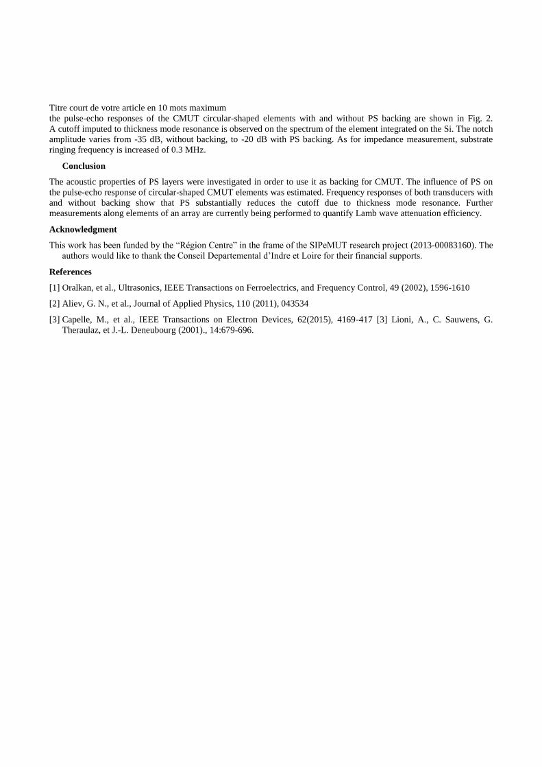
FIG. 1 – Left, Cartoon of a pSiNp loaded/chemically conjugated with different amino-acids moieties for the complexation
of pDNA. Right, TEM image of a “loaded-free” pSiNp, bearing pores.
[1] Salonen J., Laitinen L., Kaukonen A. M. et al. Mesoporous silicon microparticles for oral drug delivery: loading and
release of five model drugs. J. Control. Release 108, 362–374 (2005).
[2] Bimbo L. M., Sarparanta M., Santos H. A. et al. Biocompatibility of thermally hydrocarbonized porous silicon
nanoparticles and their biodistribution in rats. ACS Nano 4, 3023–3032 (2010).
[3] Canham L. T. Silicon quantum wire array fabrication by electrochemical and chemical dissolution of wafers. Appl.
Phys. Lett. 57, 1046–1048 (1990).
[4] Chen S., Ni B., Huang, H., Chen X., Ma H. siRNA-loaded PEGylated porous silicon nanoparticles for lung cancer
therapy. J. Nanopart. Res. 16, 2648-2656 (2014)
[5] Secret E., Maynadier M., Gallud A., Chaix A. Bouffard E., Gary-Bobo M., Marcotte N., Mongin O., El Cheikh K.,
Hugues V., Auffan M., Frochot C., Morère A., Maillard P., Blanchard-Desce M., Sailor M. J., Garcia M., Durand J.
O., Cunin F. Adv. Mater. 26, 7643-7648 (2014)
Nanotopography of porous silicon scaffold to increase bone regeneration.
Naveen Fatima*, Elodie Middendorp*
Eduardo Jose Cueto Diaz**, Alban Desoutter*
Hamideh Salehi*, Frédérique Cunin**, Frédéric Cuisinier*, Pierre-Yves Collart Dutilleul*
* Laboratoire Bioingénierie et Nanosciences (LBN) 545 avenue Pr JL VIALA 34193 Montpellier Cedex 5 France –
** Institut Charles Gerhardt Montpellier, UMR 5253 CNRS-ENSCM-UM2-UM1, Université de Montpellier.
2 place Eugène Bataillon, 34095 Montpellier Cedex 05 France – [email protected]
Abstract :
Porous silicon (pSi) is a synthetic mineral biomaterial which is chemically and mechanically tunable. Its
biocompatibility has been extensively studied in vitro and in vivo for drug delivery and tissue engineering. PSi degrades
into silicic acid which is a natural biologically active compound with osteogenic effects. PSi microparticles along with
dental pulp stem cells (DPSC) offer a promising scope for bone regeneration, as previous experiments using mesoporous
silicon wafer and DPSCs have already proved its efficiency to support stem cells growth and osteodifferentiation.
Understanding the kinetics of pSi degradation is especially important for in vivo applications.
The aim of this research was to assess porous silicon microparticles as a bioactive scaffold for bone tissue engineering
and degradation kinetics of porous silicon microparticles to evaluate it as a bioactive scaffold for bone tissue engineering,
promoting both human stem cell adhesion and osteodifferentiation. This study focuses on particles resorption during
bone formation.
PSi particles, ranging from 50-200µm were created by electrochemical etching. Kinetics of pSi microparticles
degradation was studied in vitro and in vivo. Particles resorption were followed in vitro in ddH2O, PBS and culture
medium, and in vivo after implantation in rat tail vertebrae. Release of silicic acid from the pSi microparticles was
analyzed by ICP-MS (inductively coupled plasma mass spectroscopy). For bone tissue formation, pSi particles and
DPSC were incubated in vitro to produce a bone-like matrix and evaluated by histology and Raman spectroscopy. This
process was then followed in vivo, in rats, and investigated by µCT and histology.
ICP-MS revealed significantly sustained amount of silicic acid release from thermally oxidized pSi microparticles
compared to non-oxidized pSi microparticles in PBS, during 45 days. And in vitro osteodifferentiation assays, with
DPSC incubated on pSi demonstrated an increase of microcalcifications (Alizarin red staining) and collagen fibers
formation (Raman spectroscopy). Enhanced bone regeneration was confirmed in vivo, with higher bone volume and
mineral density in rat’s bone defects treated by pSi-DPSC (µCT). Histological evaluation showed the presence of
remaining particles after 1 month, with mineralized collagen around particles. After 2 months, pSi particles were
completely resorbed and replaced by newly formed bone.
This work was conducted in the perspective of specific clinical conditions. Indeed, biodegradability and
biocompatibility are not constitutive properties of the material and are dependent on the site of implantation. This work
provides positive clue for pSi-DPSC graft to regenerate bone, especially in case of sever alveolar ridge resorption where
dental rehabilitation is inconceivable or when dental implant provision is not possible due to insufficient amount of bone.
Our in vivo results showed that pSi, along with DPSC, is able regenerate bone and increase the vertical height of resorbed
alveolar ridges, allowing possibilities of further dental treatment. Furthermore, in our experimental model of large bony
defect, pSi-DPSC appeared to be efficient scope to regenerate bone tissue, even in inflammatory environment following
bone injury.
Références :
[1] Salehi H, Collart-Dutilleul PY, Gergely C, Cuisinier FJ. (2015). Confocal Raman microscopy to monitor
extracellular matrix during dental pulp stem cells differentiation. J Biomed Opt. 20(7):076013.
[2] Collart-Dutilleul PY, Panayotov I, Secret E, Cunin F, Gergely C, Cuisinier F, Martin M. (2014). Initial stem cell
adhesion on porous silicon surface: molecular architecture of actin cytoskeleton and filopodial growth. Nanoscale Res
Lett 9(1):564.
[3] Collart-Dutilleul PY, Secret E, Panayotov I, Deville de Périère D, Martín-Palma RJ, Torres-Costa V, Martin M,
Gergely C, Durand JO, Cunin F, Cuisinier FJ. (2012). Adhesion and proliferation of human mesenchymal stem cells
from dental pulp on porous silicon scaffolds. ACS Appl Mater Interfaces 6(3):1719-28.
[4] Collart-Dutilleul PY, Chaubron F, De Vos J, Cuisinier FJ. (2015). Allogenic banking of dental pulp stem cells for
innovative therapeutics. World J Stem Cells 7(7):1010-21.

…………………………………………………………………………………………………………………………………………………………………………………………………………………………………………………………….
…………………………………………………………………………………………………………………………………………………………………………………………………………………………………………………………….
…………………………………………………………………………………………………………………………………………………………………………………………………………………………………………………………….
…………………………………………………………………………………………………………………………………………………………………………………………………………………………………………………………….
…………………………………………………………………………………………………………………………………………………………………………………………………………………………………………………………….
…………………………………………………………………………………………………………………………………………………………………………………………………………………………………………………………….
…………………………………………………………………………………………………………………………………………………………………………………………………………………………………………………………….
…………………………………………………………………………………………………………………………………………………………………………………………………………………………………………………………….
…………………………………………………………………………………………………………………………………………………………………………………………………………………………………………………………….
…………………………………………………………………………………………………………………………………………………………………………………………………………………………………………………………….
…………………………………………………………………………………………………………………………………………………………………………………………………………………………………………………………….
…………………………………………………………………………………………………………………………………………………………………………………………………………………………………………………………….
…………………………………………………………………………………………………………………………………………………………………………………………………………………………………………………………….
…………………………………………………………………………………………………………………………………………………………………………………………………………………………………………………………….
…………………………………………………………………………………………………………………………………………………………………………………………………………………………………………………………….
…………………………………………………………………………………………………………………………………………………………………………………………………………………………………………………………….
…………………………………………………………………………………………………………………………………………………………………………………………………………………………………………………………….
…………………………………………………………………………………………………………………………………………………………………………………………………………………………………………………………….
…………………………………………………………………………………………………………………………………………………………………………………………………………………………………………………………….
…………………………………………………………………………………………………………………………………………………………………………………………………………………………………………………………….
…………………………………………………………………………………………………………………………………………………………………………………………………………………………………………………………….
…………………………………………………………………………………………………………………………………………………………………………………………………………………………………………………………….
…………………………………………………………………………………………………………………………………………………………………………………………………………………………………………………………….
…………………………………………………………………………………………………………………………………………………………………………………………………………………………………………………………….
…………………………………………………………………………………………………………………………………………………………………………………………………………………………………………………………….
…………………………………………………………………………………………………………………………………………………………………………………………………………………………………………………………….
…………………………………………………………………………………………………………………………………………………………………………………………………………………………………………………………….
…………………………………………………………………………………………………………………………………………………………………………………………………………………………………………………………….
…………………………………………………………………………………………………………………………………………………………………………………………………………………………………………………………….
…………………………………………………………………………………………………………………………………………………………………………………………………………………………………………………………….
…………………………………………………………………………………………………………………………………………………………………………………………………………………………………………………………….
…………………………………………………………………………………………………………………………………………………………………………………………………………………………………………………………….
…………………………………………………………………………………………………………………………………………………………………………………………………………………………………………………………….
…………………………………………………………………………………………………………………………………………………………………………………………………………………………………………………………….
…………………………………………………………………………………………………………………………………………………………………………………………………………………………………………………………….
…………………………………………………………………………………………………………………………………………………………………………………………………………………………………………………………….
…………………………………………………………………………………………………………………………………………………………………………………………………………………………………………………………….
…………………………………………………………………………………………………………………………………………………………………………………………………………………………………………………………….
…………………………………………………………………………………………………………………………………………………………………………………………………………………………………………………………….
…………………………………………………………………………………………………………………………………………………………………………………………………………………………………………………………….
…………………………………………………………………………………………………………………………………………………………………………………………………………………………………………………………….
…………………………………………………………………………………………………………………………………………………………………………………………………………………………………………………………….
…………………………………………………………………………………………………………………………………………………………………………………………………………………………………………………………….
…………………………………………………………………………………………………………………………………………………………………………………………………………………………………………………………….
…………………………………………………………………………………………………………………………………………………………………………………………………………………………………………………………….
…………………………………………………………………………………………………………………………………………………………………………………………………………………………………………………………….
…………………………………………………………………………………………………………………………………………………………………………………………………………………………………………………………….
…………………………………………………………………………………………………………………………………………………………………………………………………………………………………………………………….
…………………………………………………………………………………………………………………………………………………………………………………………………………………………………………………………….
NOTES :