near-field scattered by a single nanoslit in a metal film
TRANSCRIPT
Near-field scattered by a single nanoslit in a metal film
Lionel Aigouy,1,* Philippe Lalanne,2 Haitao Liu,2,3 Gwénaelle Julié,4 Véronique Mathet,4
and Michel Mortier5
1Laboratoire Photons Et Matière, UPR CNRS A0005, Ecole Supérieure de Physique et de Chimie Industrielles (ESPCI),10 rue Vauquelin, 75231 Paris Cedex 5, France
2Laboratoire Charles Fabry de l’Institut d’Optique, University Paris-Sud, CNRS, Campus Polytechnique, RD 128,91127 Palaiseau cedex, France
3Key Laboratory of Opto-Electronic Information Science and Technology, Ministry of Education,Institute of Modern Optics, Nankai University, Tianjin 300071, China
4Institut d’Electronique Fondamentale, UMR CNRS 8622, Bâtiment 220�221, Université Paris-Sud,91405 Orsay Cedex, France
5Laboratoire de Chimie de la Matière Condensée de Paris, UMR CNRS 7574, Ecole Nationale Supérieure de Chimie deParis (ENSCP), Rue Pierre et marie Curie, 75231 Paris Cedex 5, France
*Corresponding author: [email protected]
Received 27 August 2007; accepted 22 October 2007;posted 1 November 2007 (Doc. ID 86922); published 13 December 2007
Using a scanning near-field optical microscope, we visualize, in three dimensions, the electromagneticfield distribution near an isolated slit aperture in a thin gold film. At the metal-air interface and fora TM incident polarization, we confirm some recently observed results and show that the slit gener-ates two kinds of surface waves: a slowly decaying surface plasmon polariton and a quasi-cylindricalwave that decreases more rapidly when moving away from the slit. These waves are not generated fora TE incident polarization. In a noncontact mode, we also observe how the transmitted light divergesin free space. At a small distance from the slit �� 2 �m�, we find that the emerging light spreads in alldirections for TM, forming an electromagnetic cloud, whereas it is concentrated above the slit for TE,forming a more directive light jet. The experimental images are in good agreement with the numericalsimulations. © 2007 Optical Society of America
OCIS codes: 240.6680, 050.1220.
Light scattering by nanoapertures in thin noblemetal films has recently been widely studied by scan-ning near-field optical microscopy (SNOM) and otherunconventional techniques [1–5]. The interest insuch a microscopic characterization is motivated byunderstanding the physics hidden behind the surfacewaves generation, their propagation, and their inter-action with the local environment [6], but also by thedesign of new photonic and plasmonic devices or sen-sors [7,8]. Since the usually observed effects dependon many geometrical parameters of the apertures,such as their shape, their size, and their relativedistance, the comprehension of basic phenomena canbe eased by studying elementary structures, such as
nanoholes or nanoslits, isolated on the metal surfaceor simply coupled two by two to minimize the numberof varying parameters.
In this paper, we perform a study of the near-fielddistribution around an isolated nanoslit aperture as afunction of the incident polarization direction. Wewill confirm some recently observed results thatshowed that the surface waves generated by nanoslitapertures in a metal film are the sum of two kinds ofwave: a surface plasmon polariton (SPP) and anothernonplasmonic quasi-cylindrical wave that decays at amuch faster rate [4,9–11]. In contrast with previousnear- and far-field measurements, the waves are di-rectly visualized, without involving any multiple in-terference phenomena with the light transmittedthrough the substrate [1,3], with another SPP [2,4] orby far-field interferometry [10–12]. By performingscans in a noncontact mode in a plane perpendicular
0003-6935/07/368573-05$15.00/0© 2007 Optical Society of America
20 December 2007 � Vol. 46, No. 36 � APPLIED OPTICS 8573
to the surface and to the slit axis, we have also beenable to observe how the light diverges in the far-fieldfor both polarizations. At a short distance from theaperture �� 2 �m�, the light emerging from the slitspreads in all directions for TM forming an electro-magnetic cloud, whereas it is much more directionalfor TE forming a narrow beam above the slit.
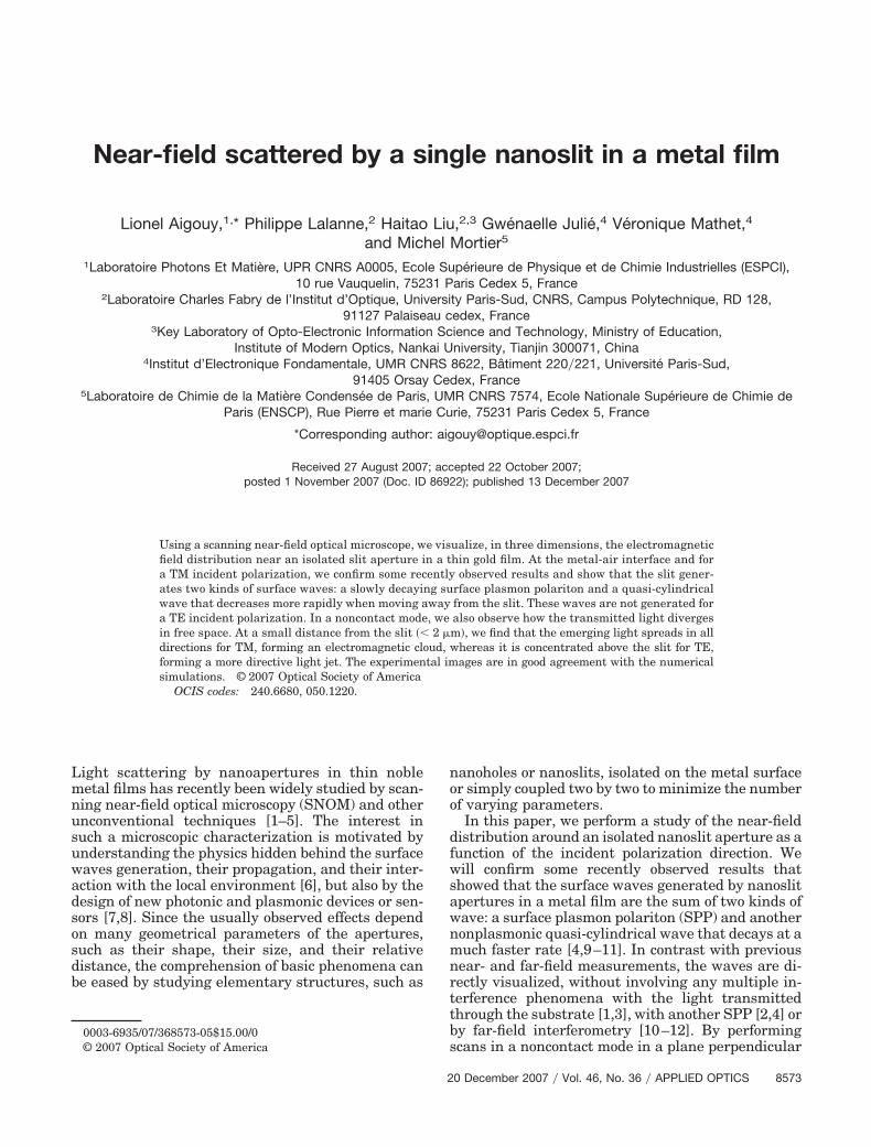
The sample consists of a slit aperture (width� 350 nm, length � 20 �m) made in a 100 nm thickgold film on a fused silica substrate by electron-beamlithography and subsequent ion-beam etching. A5 nm thick chromium layer was sputtered on theglass prior to the gold deposition to ensure good ad-hesion. A scanning electron microscope image (SEM)of the structure is shown in Fig. 1, with a sketch of theexperimental setup. The SNOM apparatus used inthis study is different from the configurations usuallyemployed in near-field optics (see, for instance, [1–3]and [13–15]). It uses a fluorescent particle glued atthe end of an atomic force microscope tip to detect thelocal electromagnetic field [16]. Although unusual,the fluorescence of films deposited on metal surfaceshas recently been employed by several groups to de-tect surface plasmon fields with far-field microscopytechniques [17,18]. In the present case, the fluores-cent material has a subwavelength size ��300 nm�,providing a lateral resolution in the order of ��3. It ismade of an erbium�ytterbium codoped fluoride glass,highly fluorescent, and chemically stable. The com-pound is excited in the near-infrared �� � 975 nm�and the fluorescence that involves a nonlinear ab-sorption process called up-conversion is collected inthe visible range �530–550 nm�. Under such excita-tion, we therefore expect to detect the square of theelectromagnetic field intensity. Besides, since thematerial structure is amorphous, the probe is sensi-tive to all components of the electromagnetic field,giving a representation of the total electric field onthe surface. Under direct illumination by a laserbeam, the particles can emit up to 106–107 photonsper s, offering a good signal-to-noise ratio. For theexperiments, the tip is scanned above the samplewith an XYZ piezoelectric stage, and both the sample
and illumination remain static. The tip is movable inall three directions allowing scans to be performedeither on the surface (XY mode) or in planes perpen-dicular to the sample (XZ or YZ modes). For a XY-type scan, the tip�sample distance is maintainedconstant in the tapping mode (oscillation amplitude�10–20 nm) with a feedback loop. For the XZ- orYZ-type scans, the feedback loop is disabled and thetip freely moves above the sample. The latter is illu-minated from the rear side by a 975 nm laser diodepolarized in a direction either parallel (TE) or per-pendicular (TM) to the slit axis. The incident beam isonly weakly focused, so that the entire slit is illumi-nated.
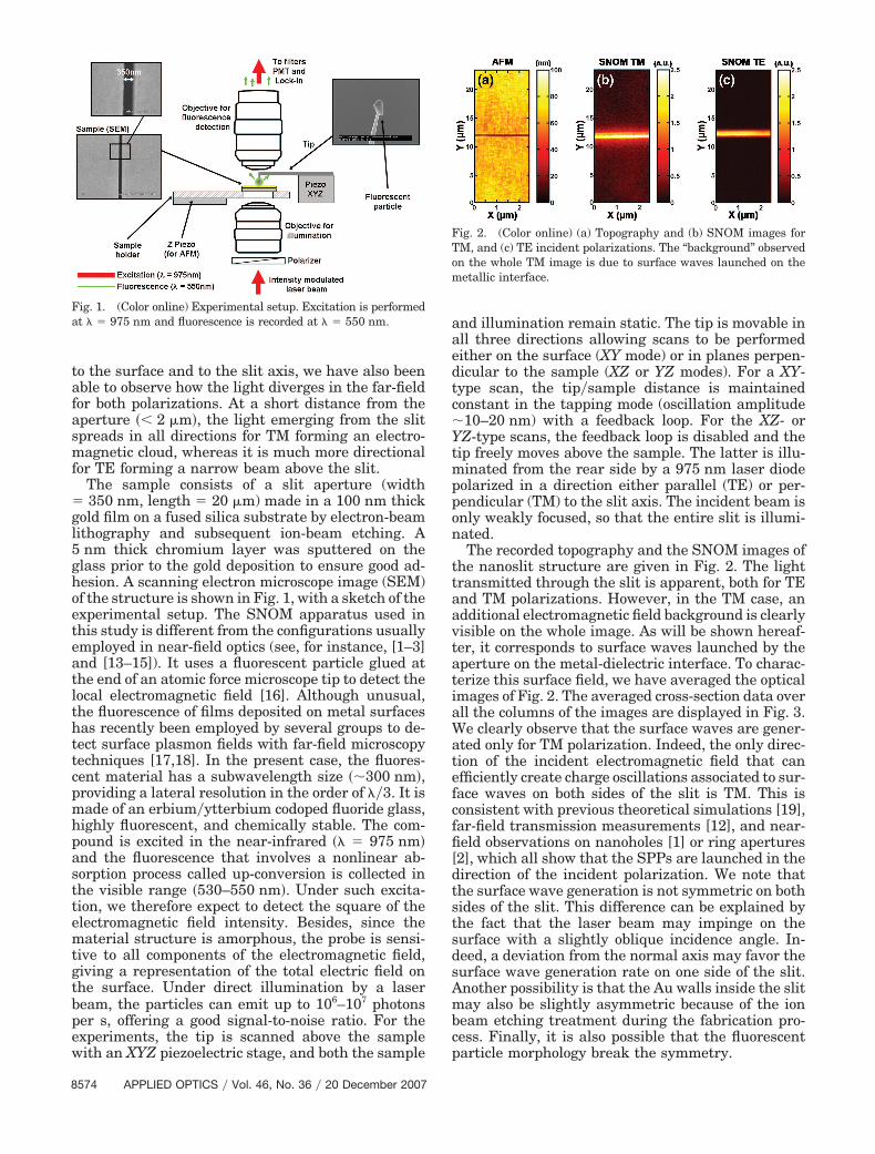
The recorded topography and the SNOM images ofthe nanoslit structure are given in Fig. 2. The lighttransmitted through the slit is apparent, both for TEand TM polarizations. However, in the TM case, anadditional electromagnetic field background is clearlyvisible on the whole image. As will be shown hereaf-ter, it corresponds to surface waves launched by theaperture on the metal-dielectric interface. To charac-terize this surface field, we have averaged the opticalimages of Fig. 2. The averaged cross-section data overall the columns of the images are displayed in Fig. 3.We clearly observe that the surface waves are gener-ated only for TM polarization. Indeed, the only direc-tion of the incident electromagnetic field that canefficiently create charge oscillations associated to sur-face waves on both sides of the slit is TM. This isconsistent with previous theoretical simulations [19],far-field transmission measurements [12], and near-field observations on nanoholes [1] or ring apertures[2], which all show that the SPPs are launched in thedirection of the incident polarization. We note thatthe surface wave generation is not symmetric on bothsides of the slit. This difference can be explained bythe fact that the laser beam may impinge on thesurface with a slightly oblique incidence angle. In-deed, a deviation from the normal axis may favor thesurface wave generation rate on one side of the slit.Another possibility is that the Au walls inside the slitmay also be slightly asymmetric because of the ionbeam etching treatment during the fabrication pro-cess. Finally, it is also possible that the fluorescentparticle morphology break the symmetry.
Fig. 1. (Color online) Experimental setup. Excitation is performedat � � 975 nm and fluorescence is recorded at � � 550 nm.
Fig. 2. (Color online) (a) Topography and (b) SNOM images forTM, and (c) TE incident polarizations. The “background” observedon the whole TM image is due to surface waves launched on themetallic interface.
8574 APPLIED OPTICS � Vol. 46, No. 36 � 20 December 2007
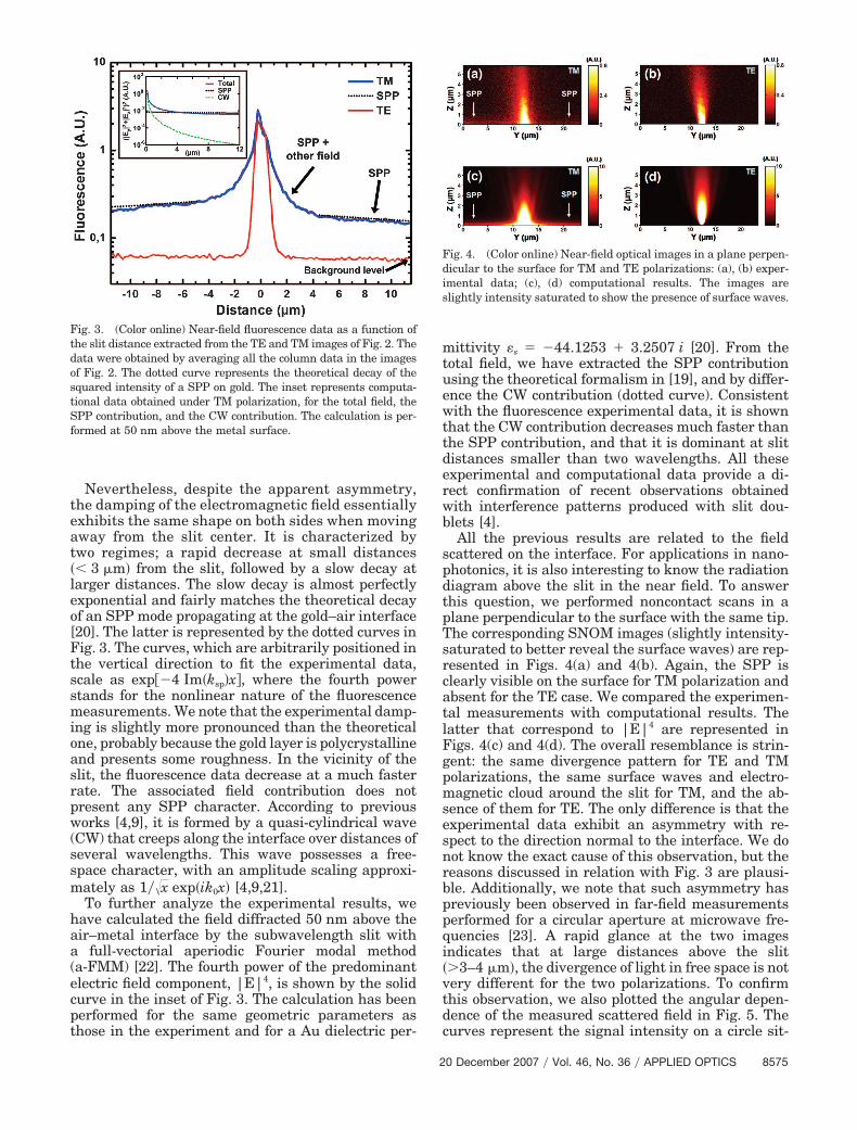
Nevertheless, despite the apparent asymmetry,the damping of the electromagnetic field essentiallyexhibits the same shape on both sides when movingaway from the slit center. It is characterized bytwo regimes; a rapid decrease at small distances�� 3 �m� from the slit, followed by a slow decay atlarger distances. The slow decay is almost perfectlyexponential and fairly matches the theoretical decayof an SPP mode propagating at the gold–air interface[20]. The latter is represented by the dotted curves inFig. 3. The curves, which are arbitrarily positioned inthe vertical direction to fit the experimental data,scale as exp��4 Im�ksp�x�, where the fourth powerstands for the nonlinear nature of the fluorescencemeasurements. We note that the experimental damp-ing is slightly more pronounced than the theoreticalone, probably because the gold layer is polycrystallineand presents some roughness. In the vicinity of theslit, the fluorescence data decrease at a much fasterrate. The associated field contribution does notpresent any SPP character. According to previousworks [4,9], it is formed by a quasi-cylindrical wave(CW) that creeps along the interface over distances ofseveral wavelengths. This wave possesses a free-space character, with an amplitude scaling approxi-mately as 1��x exp�ik0x� [4,9,21].
To further analyze the experimental results, wehave calculated the field diffracted 50 nm above theair–metal interface by the subwavelength slit witha full-vectorial aperiodic Fourier modal method(a-FMM) [22]. The fourth power of the predominantelectric field component, |E|4, is shown by the solidcurve in the inset of Fig. 3. The calculation has beenperformed for the same geometric parameters asthose in the experiment and for a Au dielectric per-
mittivity �s � �44.1253 � 3.2507 i [20]. From thetotal field, we have extracted the SPP contributionusing the theoretical formalism in [19], and by differ-ence the CW contribution (dotted curve). Consistentwith the fluorescence experimental data, it is shownthat the CW contribution decreases much faster thanthe SPP contribution, and that it is dominant at slitdistances smaller than two wavelengths. All theseexperimental and computational data provide a di-rect confirmation of recent observations obtainedwith interference patterns produced with slit dou-blets [4].
All the previous results are related to the fieldscattered on the interface. For applications in nano-photonics, it is also interesting to know the radiationdiagram above the slit in the near field. To answerthis question, we performed noncontact scans in aplane perpendicular to the surface with the same tip.The corresponding SNOM images (slightly intensity-saturated to better reveal the surface waves) are rep-resented in Figs. 4(a) and 4(b). Again, the SPP isclearly visible on the surface for TM polarization andabsent for the TE case. We compared the experimen-tal measurements with computational results. Thelatter that correspond to |E|4 are represented inFigs. 4(c) and 4(d). The overall resemblance is strin-gent: the same divergence pattern for TE and TMpolarizations, the same surface waves and electro-magnetic cloud around the slit for TM, and the ab-sence of them for TE. The only difference is that theexperimental data exhibit an asymmetry with re-spect to the direction normal to the interface. We donot know the exact cause of this observation, but thereasons discussed in relation with Fig. 3 are plausi-ble. Additionally, we note that such asymmetry haspreviously been observed in far-field measurementsperformed for a circular aperture at microwave fre-quencies [23]. A rapid glance at the two imagesindicates that at large distances above the slit��3–4 �m�, the divergence of light in free space is notvery different for the two polarizations. To confirmthis observation, we also plotted the angular depen-dence of the measured scattered field in Fig. 5. Thecurves represent the signal intensity on a circle sit-
Fig. 3. (Color online) Near-field fluorescence data as a function ofthe slit distance extracted from the TE and TM images of Fig. 2. Thedata were obtained by averaging all the column data in the imagesof Fig. 2. The dotted curve represents the theoretical decay of thesquared intensity of a SPP on gold. The inset represents computa-tional data obtained under TM polarization, for the total field, theSPP contribution, and the CW contribution. The calculation is per-formed at 50 nm above the metal surface.
Fig. 4. (Color online) Near-field optical images in a plane perpen-dicular to the surface for TM and TE polarizations: (a), (b) exper-imental data; (c), (d) computational results. The images areslightly intensity saturated to show the presence of surface waves.
20 December 2007 � Vol. 46, No. 36 � APPLIED OPTICS 8575
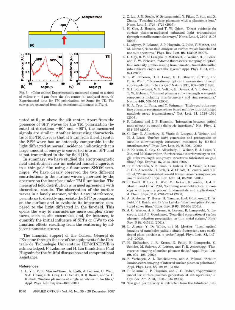
uated at 5 �m above the slit center. Apart from thepresence of SPP waves for the TM polarization (lo-cated at directions �90° and �90°), the measuredsignals are similar. Another interesting characteris-tic of the TM curve is that at 5 �m from the slit centerthe SPP wave has an intensity comparable to thelight diffracted at normal incidence, indicating that alarge amount of energy is converted into an SPP andis not transmitted in the far field [19].
In summary, we have studied the electromagneticfield distribution near an isolated nanoslit aperturein a thin gold film using a fluorescent SNOM tech-nique. We have clearly observed the two differentcontributions to the surface waves generated by theaperture on the interface under TM illumination. Themeasured field distribution is in good agreement withtheoretical results. The observation of the surfacewaves in a lonely manner, without any interference,permits us to directly appreciate the SPP propagationon the surface and to evaluate its importance com-pared to the light diffracted in the far-field. Thisopens the way to characterize more complex struc-tures, such as slit ensembles, and, for instance, toquantify the initial influence of SPPs or CWs to col-limation effects resulting from the scattering by ad-jacent nanostructures.
The financial support of the Conseil Général del’Essonne through the use of the equipment of the Cen-trale de Technologie Universtaire IEF-MINERVE isacknowledged. P. Lalanne and H. Liu thank Jean-PaulHugonin for the fruitful discussions and computationalassistance.
References1. L. Yin, V. K. Vlasko-Vlasov, A. Rydh, J. Pearson, U. Welp,
S.-H. Chang, S. K. Gray, G. C. Schatz, D. B. Brown, and W. C.Kinball, “Surface plasmons at single nanoholes in Au films,”Appl. Phys. Lett. 85, 467–469 (2004).
2. Z. Liu, J. M. Steele, W. Srituravanich, Y. Pikus, C. Sun, and X.Zhang, “Focusing surface plasmons with a plasmonic lens,”Nano. Lett. 5, 1726–1729 (2005).
3. H. Gao, J. Henzie, and T. W. Odom, “Direct evidence forsurface plasmon-mediated enhanced light transmissionthrough metallic nanohole arrays,” Nano. Lett. 6, 2104–2108(2006).
4. L. Aigouy, P. Lalanne, J. P. Hugonin, G. Julié, V. Mathet, andM. Mortier, “Near-field analysis of surface waves launched atnanoslit apertures,” Phys. Rev. Lett. 98, 153902 (2007).
5. G. Gay, B. V. de Lesegno, R. Mathevet, J. Weiner, H. J. Lezec,and T. W. Ebbesen, “Atomic fluorescence mapping of opticalfield intensity profiles issuing from nanostructured slits milledinto subwavelength metallic layers,” Appl. Phys. B 81, 871–874 (2005).
6. T. W. Ebbesen, H. J. Lezec, H. F. Ghaemi, T. Thio, andP. A. Wolff, “Extraordinary optical transmission throughsub-wavelength hole arrays,” Nature 391, 667–669 (1998).
7. S. I. Bozhevolnyi, V. S. Volkov, E. Devaux, J. Y. Laluet, andT. W. Ebbesen, “Channel plasmon subwavelength waveguidecomponents including interferometers and ring resonators,”Nature 440, 508–511 (2006).
8. K. A. Tetz, L. Pang, and Y. Fainman, “High-resolution sur-face plasmon resonance sensor based on linewidth-optimizednanohole array transmittance,” Opt. Lett. 31, 1528–1530(2006).
9. P. Lalanne and J. P. Hugonin, “Interaction between opticalnano-objects at metallo-dielectric interfaces,” Nat. Phys. 2,551–556 (2006).
10. G. Gay, O. Alloschery, B. Viaris de Lesegno, J. Weiner, andH. J. Lezec, “Surface wave generation and propagation onmetallic subwavelength structures measured by far-fieldinterferometry,” Phys. Rev. Lett. 96, 213901 (2006).
11. F. Kalkum, G. Gay, O. Alloschery, J. Weiner, H. J. Lezec, Y.Xie, and M. Mansuripur, “Surface-wave interferometry on sin-gle subwavelength slit-groove structures fabricated on goldfilms,” Opt. Express 15, 2613–2621 (2007).
12. H. F. Schouten, N. Kuzmin, G. Dubois, T. D. Visser, G. Gbur,P. F. A. Alkemade, H. Blok, G. W.’t Hooft, D. Lenstra, and E. R.Elliel, “Plasmon-assisted two-slit transmission: Young’s exper-iment revisited,” Phys. Rev. Lett. 94, 053901 (2005).
13. B. Hecht, B. Sick, U. Wild, V. Deckert, R. Zenobi, O. J. F.Martin, and D. W. Pohl, “Scanning near-field optical micros-copy with aperture probes: fundamentals and applications,”J. Chem. Phys. 112, 7761–7774 (2000).
14. A. Bouhelier, T. Huser, H. Tamaru, H.-J. Güntherodt, D. W.Pohl, F. I. Baida, and D. Van Labeke, “Plasmon optics of struc-tured silver films,” Phys. Rev. B 63, 155404 (2001).
15. J. C. Weeber, J. R. Krenn, A. Dereux, B. Lamprecht, Y. La-croute, and J. P. Goudonnet, “Near-field observation of surfaceplasmon polariton propagation on thin metal stripes,” Phys.Rev. B 64, 045411 (2001).
16. L. Aigouy, Y. De Wilde, and M. Mortier, “Local opticalimaging of nanoholes using a single fluorescent rare-earth-doped glass particle as a probe,” Appl. Phys. Lett. 83, 147–149 (2003).
17. H. Ditlbacher, J. R. Krenn, N. Felidj, B. Lamprecht, G.Schider, M. Salerno, A. Leitner, and F. R. Aussenegg, “Fluo-rescence imaging of surface plasmon fields,” Appl. Phys. Lett.80, 404–406 (2002).
18. E. Verhagen, A. L. Tchebotareva, and A. Polman, “Erbiumluminescence imaging of infrared surface plasmon polaritons,”Appl. Phys. Lett. 88, 121121 (2006).
19. P. Lalanne, J. P. Hugonin, and J. C. Rodier, “Approximatemodel for surface-plasmon generation at slit apertures,” J.Opt. Soc. Am. A 23, 1608–1615 (2006).
20. The gold permittivity is extracted from the tabulated data
Fig. 5. (Color online) Experimentally measured signal on a circleof radius r � 5 �m from the slit center (a) analyzed zone. (b)Experimental data for TM polarization. (c) Same for TE. Thecurves are extracted from the experimental images in Fig. 4.
8576 APPLIED OPTICS � Vol. 46, No. 36 � 20 December 2007

in E. D. Palik, Handbook of Optical Constants of Solids(Academic Press, 1985), Part II(1).
21. L. Chen, J. T. Robinson, and M. Lipson, “Role of radiation andsurface plasmon polaritons in the optical interactions betweena nano-slit and a nano-groove on a metal surface,” Opt. Ex-press 14, 12629–12636 (2006).
22. E. Silberstein, P. Lalanne, J. P. Hugonin, and Q. Cao, “Use of
grating theories in integrated optics,” J. Opt. Soc. Am. A 18,2865–2875 (2001).
23. M. J. Lockyear, A. P. Hibbins, J. R. Sambles, and C. R. Law-rence, “Surface-topography-induced enhanced transmissionand directivity of microwave radiation through a subwave-length circular metal aperture,” Appl. Phys. Lett. 84, 2040–2042 (2004).
20 December 2007 � Vol. 46, No. 36 � APPLIED OPTICS 8577