in electronics & communication engineering
TRANSCRIPT
DDEESSIIGGNN AANNDD VVEERRIIFFIICCAATTIIOONN OOFF WWIISSHHBBOONNEE BBUUSS IINNTTEERRFFAACCEE FFOORR SSOOCC IINNTTEEGGRRAATTIIOONN
A thesis submitted in partial fulfilment of the requirements for the degree of
Master of Technology (Research) in
Electronics & Communication Engineering
By
Ayas Kanta Swain
Roll No: 60609001
Under the supervision of
Dr. KamalaKanta Mahapatra Professor
Department of Electronics & Communication Engineering National Institute of Technology, Rourkela, Orissa
January 2010

Dedicated to my family

T
W
N
6
E
w
T
T
el
In
T
T
b
This is to
WISHBON
National Ins
0609001 for
Electronics &
work carried
The candida
The thesis, w
lsewhere fo
n my opini
Technology
To the best
ehaviour.
DNAT
certify tha
NE Bus In
stitute of T
r the award
& Commun
d out by him
ate has fulfi
which is ba
or a degree/
on, the thes
(Research)
of my kno
DepartmentTIONAL IN
at the thes
nterface f
Technology
d of the deg
nication En
m under m
illed all the
ased on can
/diploma.
sis is of sta
degree in E
owledge, h
DepartmeNAT
t of ElectronNSTITUTE
sis titled “
for SOC
y, Rourkela
gree of Ma
ngineering,
y supervisi
prescribed
ndidate’s ow
andard requ
Electronics
he bears a g
ent of ElectroTIONAL IN
CERTIFIC
nics & Com OF TECHN
ORIS
“Design a
Integratio
by Ayas K
aster of Tec
, is a bonaf
ion and gui
d requireme
wn work, h
uired for th
& Commu
good mora
Pro
onics & ComNSTITUTE
RouE
CATE
mmunicationNOLOGY, SSA, INDIA
and Verif
on” subm
Kanta Swa
chnology (R
fide record
idance.
ents.
has not bee
he award of
unication En
al character
of. K. K. M
mmunicationE OF TECurkela‐769 Email: kkm
n EngineerinROURKELA
A – 769 00
fication o
itted to th
ain, Roll No
Research) i
d of researc
en submitte
f a Master o
ngineering.
r and decen
MahapatrProfesso
n EngineerinHNOLOG008 (INDIA
ng A
08
of
he
o.
in
ch
ed
of
nt
ra or ng Y A) in
ACKNOWLEDGEMENT
I would like to take this opportunity to extend my deepest gratitude to my
teacher and supervisor, Prof. K. K. Mahapatra, for his continuous encouragement and
active guidance. I am indebted to him for the valuable time he has spared for me
during this work. He is always there to meet and talk about my ideas and he is great
moral support behind me in carrying out my research work.
I am very much thankful to Prof. S. K. Patra, HOD, ECE Department for his
continuous encouragement. I am grateful to Prof. G.S.Rath, Prof.S.Meher,
Prof.T.K.Dan and Dr.D.P.Acharya, Prof. S.K.Behera, Prof. Ajit Sahoo and
Prof.B.D.Sahoo for valuable suggestions and comments during this research period.
In addition, I am grateful to Prof. A. Routray and Prof. B.S. Das, IIT
Kharagpur for giving me an opportunity to work with them; this introduced me to the
area of research and development.
I am grateful to www.opencores.org for their technical support during the
complete project period.
I need to thank my friends especially Saroj, who stands with me in all my
endeavours. And also I am thankful to him for making my thesis more representable.
In addition, let me thank all my friends Jitendra sir, Sushant, Sudeendra,
Trillochan, Sanatan, Devi, Prasanta, Karuppanan, Deepak,Arun, Tom, Soumya,
Jagannath and Peter for their great support and encouragement during the research
period. Also, I am thankful to all the non-teaching staffs of ECE Department for their
kind cooperation.
I would like to thank Department of Information Technology, Govt. of India,
for supporting me under SMDP-VLSI project.
Last but not the least; I would like to thank my parents, brother and sister for their
unconditional support and encouragement to carry out research. I am also thankful to
my sister for helping me in typing the part of my thesis. Ayas Kanta Swain

BIO-DATA
Name of the Candidate : Ayas Kanta Swain
Father’s Name : Kulamani Swain
Permanent Address :
S/o. Kulamani Swain F-17, Sector-7 Rourkela-3
Date of Birth
: 26th August 1979
Email ID : [email protected] ACADEMIC QUALIFICATION • Continuing M. Tech (Research) in Dept. of Electronics and
Communication Engineering, National Institute of Technology Rourkela, Orissa (INDIA).
• B. E. (Hons.) (Electrical Engineering), IGIT, Sarang, Utkal
University, Orissa EXPERIENCE
• Working as a Contractual Faculty, in Project “Special Man Power Development Project for VLSI Design and its Related Software” funded by DIT under MCIT, Delhi.
• Worked as a Research Engineer in DST Sponsored Project in Dept. of AG&FE. & Dept. of Electrical Engg., IIT Kharagpur
• Worked as a Guest Faculty at Dept. Elect. Engg.,IGIT Sarang, Dhenkanal, Orissa.
PUBLICATIONS: Published 01 paper in International Conferences;
ABSTRACT
The rapid development in the field of mobile communication, digital signal
processing (DSP) motivated the design engineer to integrate complex systems of
multimillion transistors in a single chip. The integration of the transistor in a single
chip greatly increases the performance of the system while reduction in system size.
Recently, there is a considerable increase in the application front in several areas of
engineering and technology. Moore’s law states that integration density gets doubled
every two years, so the complexity of the integrated circuits also increases by keeping
the used chip area constant. In order to keep pace with the levels of integration
available, design engineers have developed new methodologies and techniques to
manage the increased complexity in these large chips.
System-on-Chip (SOC) design is proposed as an extended methodology to this
problem where pre-designed and pre-verified IP cores of embedded processors,
memory blocks, interface blocks, and analog blocks are combined on a single chip
targeting a specific application. These chips may have one or more processors on
chip, a large amount of memory, bus-base architectures, peripherals, co processors,
and I/O channels. These chips integrates systems far more similar to the boards
designed ten years ago that to the chips of even a few years ago. The primary drivers
for this are the reduction of power, smaller form factor, and lower overall cost. SOC
offers many benefits such as smaller space requirements with higher performance.
Design reuse- the use of predesigned and pre-verified cores – is now the cornerstone
of SOC design. It uses reusable IP blocks that supports plug and play integration and
in turn allows huge chips to be designed at an acceptable cost, and quality.
The benefits SOC design methodology also come with challenges such as:
larger design space, higher design and prototype costs. Apart from these challenges,
the design again needs an expertise in both hardware and software levels for proper
hardware and software co-design. Another important aspect of SOC integration is the
development of a proper test methodology for post manufacturing test. All these
integration issues makes the design time consuming and also expensive.
To deal with this inherent integration problems and reduction in design cycle
time, platform based SoC design was proposed where new designs could be quickly
created from the original platform over many design derivatives. More specifically a
platform is an abstraction level that covers a number of refinements to a lower level
resulting in improvement of the design productivity. In other side, a new concept that
is gaining interest is the Open Core SoC design methodology which is based on
publishing all necessary information about the hardware. Open Core group has
provided many pre-synthesized and pre-verified hardware core for the designer under
GPL/LGPL license.
This thesis investigates the Open core based SOC design platform. Open Core
uses a standard bus WISHBONE to alleviate System-on-Chip problem. The various
issues related to Open Core WISHBONE bus interfaces are presented in this thesis.
These include WISHBONE specification, types of interconnections, WISHBONE Bus
cycles.etc. A comparison of three bus protocol has been discussed. The issues related
to design of a WISHBONE compatible IP core, Point-to-Point interconnection, shared
bus interconnection is also presented in this investigation. All the designs are
validated by XILINX ISE simulation results and real time debugging signals though
ChipScope Pro. A SOC design methodology has been presented for a proposed SOC
architecture. Afterwards a SOC architecture of 32-bit RISC CPU, memory, System
Controller, UART and PIO has been proposed and the design methodology used to
implement the SOC in FPGA has been discussed. The functionality of CPU operation
in SOC architecture is verified by simulation results and corresponding steps for
FPGA implementation of the SOC architecture with synthesis results have been
presented. Finally, application software ha been developed in C and the object file is
ported to FPGA system for validation of the SOC functionality of the SOC
architecture.
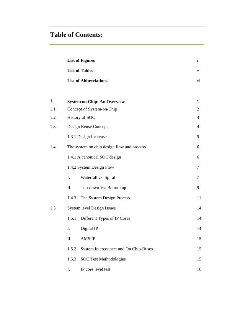
Table of Contents:
List of Figures i
List of Tables v
List of Abbreviations vi
1. System on Chip: An Overview 1
1.1 Concept of System-on-Chip 2
1.2 History of SOC 4
1.3 Design Reuse Concept 4
1.3.1 Design for reuse 5
1.4 The system on chip design flow and process 6
1.4.1 A canonical SOC design 6
1.4.2 System Design Flow 7
I. Waterfall vs. Spiral 7
II. Top-down Vs. Bottom up 9
1.4.3 The System Design Process 11
1.5 System level Design Issues 14
1.5.1 Different Types of IP Cores 14
I. Digital IP 14
II. AMS IP 15
1.5.2 System Interconnect and On Chip-Buses 15
1.5.3 SOC Test Methodologies 15
I. IP core level test 16
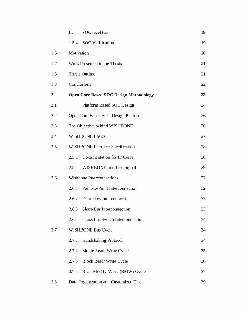
II. SOC level test 19
1.5.4 SOC Verification 19
1.6 Motivation 20
1.7 Work Presented in the Thesis 21
1.8 Thesis Outline 21
1.8 Conclusions 22
2. Open Core Based SOC Design Methodology 23
2.1 Platform Based SOC Design 24
2.2 Open Core Based SOC Design Platform 26
2.3 The Objective behind WISHBONE 26
2.4 WISHBONE Basics 27
2.5 WISHBONE Interface Specification 28
2.5.1 Documentation for IP Cores 28
2.5.1 WISHBONE Interface Signal 29
2.6. Wishbone Interconnections 32
2.6.1 Point-to-Point Interconnection 32
2.6.2 Data Flow Interconnection 33
2.6.3 Share Bus Interconnection 33
2.6.4 Cross Bar Switch Interconnection 34
2.7 WISHBONE Bus Cycle 34
2.7.1 Handshaking Protocol 34
2.7.2 Single Read/ Write Cycle 35
2.7.3 Block Read/ Write Cycle 36
2.7.4 Read-Modify-Write (RMW) Cycle 37
2.8 Data Organization and Customized Tag 39
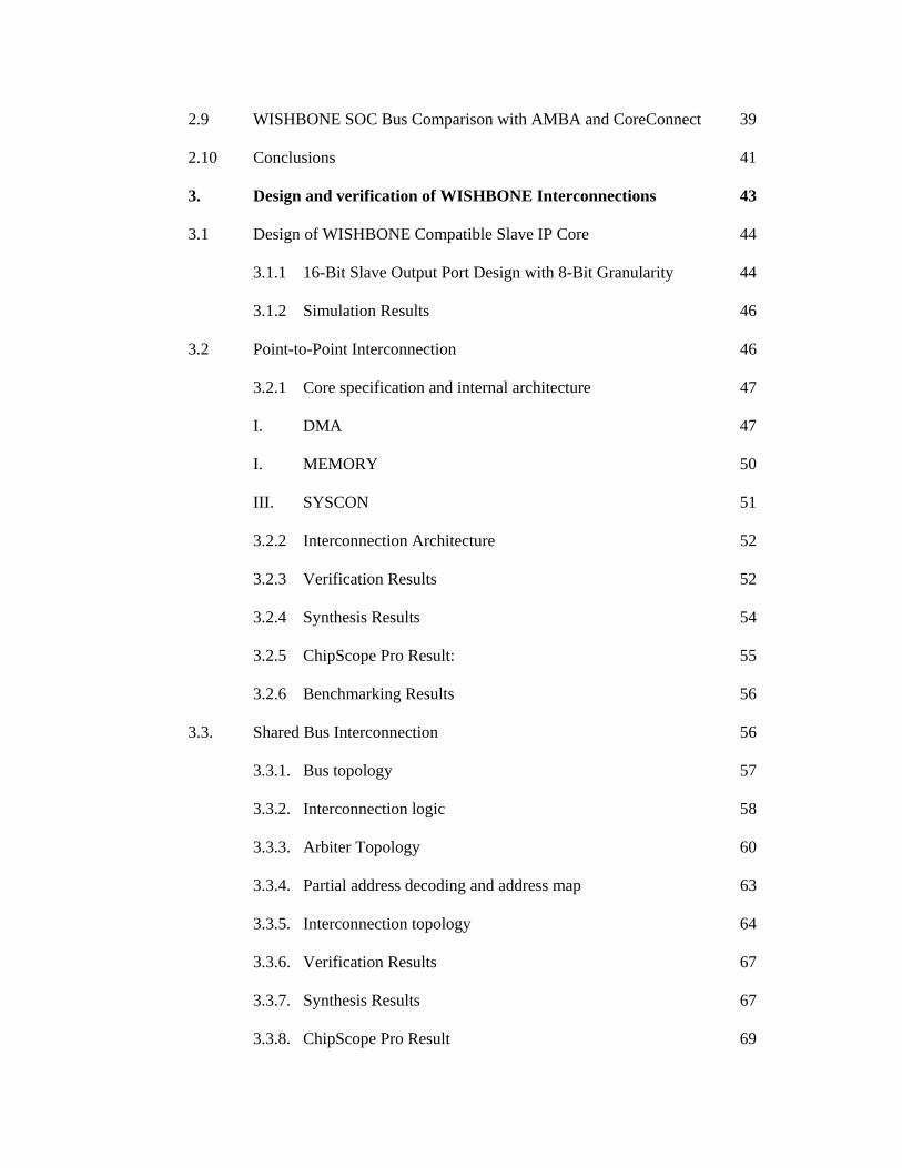
2.9 WISHBONE SOC Bus Comparison with AMBA and CoreConnect 39
2.10 Conclusions 41
3. Design and verification of WISHBONE Interconnections 43
3.1 Design of WISHBONE Compatible Slave IP Core 44
3.1.1 16-Bit Slave Output Port Design with 8-Bit Granularity 44
3.1.2 Simulation Results 46
3.2 Point-to-Point Interconnection 46
3.2.1 Core specification and internal architecture 47
I. DMA 47
I. MEMORY 50
III. SYSCON 51
3.2.2 Interconnection Architecture 52
3.2.3 Verification Results 52
3.2.4 Synthesis Results 54
3.2.5 ChipScope Pro Result: 55
3.2.6 Benchmarking Results 56
3.3. Shared Bus Interconnection 56
3.3.1. Bus topology 57
3.3.2. Interconnection logic 58
3.3.3. Arbiter Topology 60
3.3.4. Partial address decoding and address map 63
3.3.5. Interconnection topology 64
3.3.6. Verification Results 67
3.3.7. Synthesis Results 67
3.3.8. ChipScope Pro Result 69
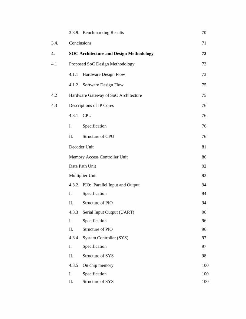
3.3.9. Benchmarking Results 70
3.4. Conclusions 71
4. SOC Architecture and Design Methodology 72
4.1 Proposed SoC Design Methodology 73
4.1.1 Hardware Design Flow 73
4.1.2 Software Design Flow 75
4.2 Hardware Gateway of SoC Architecture 75
4.3 Descriptions of IP Cores 76
4.3.1 CPU 76
I. Specification 76
II. Structure of CPU 76
Decoder Unit 81
Memory Access Controller Unit 86
Data Path Unit 92
Multiplier Unit 92
4.3.2 PIO: Parallel Input and Output 94
I. Specification 94
II. Structure of PIO 94
4.3.3 Serial Input Output (UART) 96
I. Specification 96
II. Structure of PIO 96
4.3.4 System Controller (SYS) 97
I. Specification 97
II. Structure of SYS 98
4.3.5 On chip memory 100
I. Specification 100
II. Structure of SYS 100
4.4 Conclusions 101
5. SOC Integration, Verification and FPGA Implementation 102
5.1 Integration of IP Cores 103
5.2 Verification of SOC 106
5.2.1 Verification Environment 106
5.2.2 Test Bench Development 106
5.2.3 Simulation Results 108
5.3 Synthesis results 110
5.4 FPGA Implementation 112
5.4.1 FPGA development tool and board 112 5.4.2 Interface Board Circuit Diagram 112
5.4.3 FPGA Configuration 115
5.5 ChipScope Pro Result 116
5.6 Conclusion 116
6 Application Development for SOC 117
6.1 Application Programs 118
6.2 Monitor Program Application 118
6.2.1 Algorithm for monitor program 118
6.2.2 How Monitor Program Works 122
6.3 Digital Clock Application 125
6.4 Audio Processing Application 126
6.4.1 AC97 Codec 127
6.4.2 Wishbone compatible AC97 Controller core design and Verification 129
6.5 Conclusions 132
7. Conclusions 133
7.1 Conclusions 133
7.2 Scope for Future Work 135
References 136
i
List of Figures:
Figure 1. 1 Idea of SOC design………………………………... 3 Figure 1. 2 A canonical SOC design………………………………….. 6
Figure 1. 3 Water fall design process…………………………………. 8
Figure 1. 4 Spiral Design Flow ………………………………………. 10
Figure 1. 5 Core based SOC Test Architecture………………………. 17
Figure 1. 6 Block Diagram of P1500 Wrapper for BIST DFT Core…... 18
Figure 1. 7 Integration of Cores using P1500 wrapper……………….. 19
Figure 2.1 WISHBONE Intercon
system…………………………….
27
Figure 2.2 Point to point interconnection with WISHBONE interface
signals…………………………………………………… 32
Figure 2.3(a) Point-to-Point
Interconnection…………………………….. 32
Figure 2.3(b) Data flow
Interconnection………………………………… 33
Figure: 2. 4 (a) Shared bus interconnection ………………………………. 33
Figure 2.4 (b) Crossbar switch interconnection…………………………... 33
Figure: 2. 5 Handshaking
protocol…………………………………….
35
Figure: 2. 6 (a) Single Read Cycle ………………………………………… 35
Figure: 2.6 (b) Single write
cycle…………………………………………..
35
Figure: 2. 7 (a) Block Read cycle…………………………………………. 36
Figure: 2. 7 (b)
Block Write cycle………………………………………….. 37
Figure: 2. 8 Read-Modified-Write Cycle………………………………. 38
Figure: 3. 1
Block diagram of UART………………………………….. 45
ii
Figure: 3. 2 Simulation result of 16-bit output port with 8-bit
granularity…………………………………………………
46
Figure: 3. 3 Point-to-point interconnection……………………………... 47
Figure: 3. 4 Block diagram of DMA………………………………….
48
Figure: 3. 5 Block write cycle.
………………………………………… .
49
Figure: 3. 6 Block read
cycle……………………………………………
50
Figure: 3. 7 Block diagram of memory module………………………..
51
Figure: 3. 8
Block diagram and timing diagram of SYSCON…………. 52
Figure: 3. 9
Simulation result for a clock period of 2500 ns…………..
53
Figure: 3. 10 Simulation results for a clock period of 5000
ns…………...
53
Figure: 3. 11 RTL schematic of interconnection……………………….. 54
Figure: 3. 12
ChipScope Pro results of real time signals of interconnection…………………………………….. 55
Figure: 3. 13
Multiplexed address/ data bus……………………………. 58
Figure: 3. 14
(a)
Three-state Interconnection……………………………….. 59
Figure: 3. 15 (b)
Multiplexor logic Interconnection……………………….. 59
Figure: 3. 16
Round-robin arbiter working as a rotary switch…………. 60
Figure: 3. 17
Round-robin arbiter working as a rotary switch………….. 61
Figure: 3. 18
Timing diagram of arbiter…………………………………. 62
iii
Figure: 3. 19
Block Diagram of a Generalized Shared bus Interconnection……………………………………………... 65
Figure: 3. 20
Simulation result for a clock period of 4000 ns……………. 67
Figure: 3. 21
RTL Schematics of shared bus interconnection……………. 68
Figure: 3. 22
ChipScope Pro results of real time signals of interconnection……………………………………………… 69
Figure: 4. 1 Design Methodology………………………………………. 74
Figure: 4. 2 Hardware gateway of SOC architecture……………………. 75
Figure: 4. 3 Block diagram of CPU…………………………………….. 77
Figure: 4. 4 Pipeline stages of CPU……………………………………. 78
Figure: 4. 5 pipeline stages of instructions……………………………. 80
Figure: 4. 6 IF Issue………………………………………………….. 80
Figure: 4. 7 Block Diagram of Decoder Unit………………………… 81
Figure: 4. 8 Basic Operation of ID Stage……………………………… 82
Figure: 4. 9 Shifting of Control Signal………………………………….. 83
Figure: 4. 10 Circuit diagram for Shifting Operation……………………... 84
Figure: 4. 11 Circuit of Detecting Register Conflict…………………… 84
Figure: 4. 12 Pipeline Control during Memory Load Contention………. 85
Figure: 4. 13 Wishbone ACK and CPU’s SLOT………………………… 86
Figure: 4. 14 Instruction Fetch Cycle…………………………………….. 88
Figure: 4. 15 Memory Access Cycle……………………………………. 89
Figure: 4. 16 IF_MA Conflict…………………………………………. 90
Figure: 4. 16 IF_MA Conflict…………………………………………. 90
Figure: 4. 17 Read modify write cycle………………………………… 91
Figure: 4. 18 Block Diagram of Data Path Unit………………………. 93
Figure: 4. 19 Block Diagram of Multiplier Unit…………………… 94
iv
Figure: 4. 20 Registers of PIO………………………………………. 95
Figure: 4. 21 UART Registers and its address……………………… 97
Figure: 4. 22 System Controller (SYS) Registers 99
Figure: 5. 1 Block Diagram of Experimental Set-Up for FPGA Implementation……………………………………………….. 107
Figure: 5. 2 Circuit diagram of interfacing board………………………….. 108
Figure: 5. 3 Experimental Set-Up pf FPGA Implementation…………….. 190
Figure: 6. 1 Flow Chart of Monitor Program………………………………… 121
Figure: 6. 2
Monitor output presented in a pictorial
form……………… 124
Figure: 6. 3
Output of Real Time Clock
Application………………….. 125
Figure: 6. 4 Block diagram of LM4550 audio codec………………… 126
Figure: 6. 5
AC link serial interface protocol…………………………. 127
Figure: 6. 6
Block Diagram of AC97 Controller
Core………………… 130
Figure: 6. 7
Real time signals of AC 97 Controller for the loop back test performed…………………………………………………
131
Figure: 6. 8
SOC Architecture for Audio Processing Application………. 131
v
List of Tables
Table: 2. 1 Master Signals 30
Table: 2. 2 Slave Signal 31 Table: 2. 3 Signals Common to both Masters and Slaves 31 Table: 2. 4 Comparison of WISHBONE, AMBA and CoreConnect 40 Table: 3. 1 Device utilization summary for Spartan3e 54 Table: 3. 2 Device utilization summary for Virtex-II Pro 55
Table: 3. 3 32-bit Point-to-Point interconnection benchmark results 56
Table: 3. 4 Address map used by Interconnection 64
Table: 3. 5 Device utilization summary of interconnection Spartan3e 68
Table: 3. 6 Device utilization summary in Virtex-II Pro 69 Table: 3. 7 32-bit shared bus interconnection benchmark results 70 Table: 4. 1 Input Output Signals of CPU 78 Table: 4. 2 Input Output Signals of PIO 95 Table: 4. 3 UART Input Output Signals 96 Table: 4. 4 Baud Rate Settings Example 97 Table: 4. 5 System Controller Input Output Signals 98 Table: 4. 6 On-chip Memory Input Output Signals 100 Table: 5. 1 Address Map of the Peripherals 104 Table: 5. 2 Top module Input Output Signals 105
Table: 5. 3 Assembly Instruction with Hex Code, Bus transaction and Output 108
Table: 5. 4 Synthesis Results with Area Optimization 111 Table: 5. 5 Synthesis Results with Speed Optimization 111 Table: 5. 6 Comparison of Synthesis Results 112 Table: 6. 1 List of Functions used in Monitor Program 119
Table: 6. 2 Device Utilization Summary for Audio Processing application 132
vi
List of Abbreviations:
SOC System on Chip
IP Intellectual Property
PBD Platform Based Design
CAD Computer Aided Design
GPL General Public License
LGPL Lesser General Public License
RTL Register Transfer Logic
VGA Video Graphics Array
UART Universal Asynchronous Receiver/Transmitter
MAC Multiply and Accumulate
PCI Peripheral Interconnect Component
VME VERSAmodule Eurocard bus
ISA Instruction Set Architecture
RISC Reduction Instruction Set Architecture
DSP Digital Signal Processing
ASIC Application Specific Integrated Circuit
FPGA Field Programmable Gate Array
VHDL VHSIC Hardware Description Language
RMW Read Modify Write
ASB Advanced System Bus
AHB Advanced High performance Bus
APB Advanced Peripheral Bus
PLB Processor Local Bus
OPB On-Chip Peripheral Bus
System-on-Chip: An Overview
1
Concept of System‐on‐Chip History of SOC Design Reuse Concept The system on chip design flow and process
System level Design Issues Motivation Work Presented in the Thesis Thesis Outline Conclusions
Chapter 1
System‐on‐Chip: An Overview
System-on-Chip: An Overview
2
This chapter describes the System-on-Chip (SOC) design concept. Various issues
related to SOC design such as “Design Reuse”, system design flow and system design
processes are discussed in this chapter. The system level issues such as on-chip buses,
SOC test methodologies and SOC verifications are also discussed. In the final section the
motivation behind the thesis, work presented in this thesis with thesis outline is
presented.
1.1 Concept of SystemonChip
The rapid development in the field of mobile communication, digital signal
processing (DSP) motivated the design engineer to integrate complex systems of
multimillion transistors in a single chip. The integration of the transistor in a single chip
greatly increases the performance of the system while reduction in system size. There is a
considerable increase in the application front in recent time. Moore’s law states that
integration density gets doubled every two years so the complexity of the integrated
systems also increases by keeping the used chip area constant. In order to keep pace with
the levels of integration available, design engineers have developed new methodologies
and techniques to manage the increased complexity in these large chips [1].
System-on-Chip (SOC) design is proposed as an extended methodology to this
problem where IP cores of embedded processors, memory blocks, interface blocks, and
analog blocks are combined on a single chip targeting a specific application. These chips
may have one or more processors on chip, a large amount of memory, bus-based
architectures, peripherals, co- processors, and I/O channels [2].These chips integrates
systems far more similar to the boards designed ten years ago that to the chips of even a
few years ago [2]. The integration process involves connecting the IP blocks to the
communication network, implementing design-for-test (DFT) techniques and using
methodologies to verify and validate the overall system-level design [1].
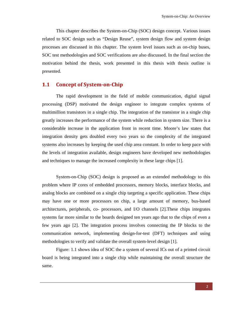
Figure: 1.1 shows idea of SOC the a system of several ICs out of a printed circuit
board is being integrated into a single chip while maintaining the overall structure the
same.
System-on-Chip: An Overview
3
The benefits of SOC design include:
• Smaller space requirements.
• Reduction in chip count.
• Lower memory requirements.
• Greater design freedom.
• Lower consumer costs.
• Higher performance and more reliable as the system will be on a single chip.
These benefits also come with challenges including:
• Larger design space, higher design and prototype costs
• A high level of debugging methodology,
• Power management,
• Longer design and prototyping cycle time
Apart from these challenges, the design again needs an expertise in both hardware and
software levels for proper hardware and software co-design. Another important aspect of
SOC integration is the development of a proper test methodology for post manufacturing
test. All these integration issues makes the design time consuming and also expensive.
Figure: 1. 1 Idea of SOC design
System-on-Chip: An Overview
4
1.2 History of SOC
In 1974 digital Watch is the first developed System-On-Chip Integrated Circuit.
The Microma liquid crystal display (LCD) digital watch is the first product to integrate a
complete electronic system onto a single silicon chip, called a System-on-Chip. The first
true SOC appeared in a Microma watch in 1974 when Peter Stoll integrated the LCD
driver transistors as well as the timing functions onto a single Intel 5810 CMOS chip
[14]. Many ASIC vendors addressed SOC opportunities in the 1990s by embedding
microcontrollers and DSPs into system-level chips that enabled hand-held games and
instruments, as well as speech processing, data communications, and PC peripheral
products.
1.3 Design Reuse Concept
With the evolution of technology, the ways of designing the chips have been
changed. It differs from the traditional design procedure such as writing the RTL from
scratch, integrating RTL blocks into a top-level designing and doing synthesis followed
by placement & routing.
Design reuse – the use of pre-designed and pre-verified cores – is now the cornerstone of
SOC design [2]. It uses reusable IP blocks that supports plug and play integration and in
turn allows huge chips to be designed at an acceptable cost, and quality. This section
discusses various issues related to design of reusable Intellectual Property (IP) core,
integration of cores to form a System on Chip design.
As Submicron technology is being used to design, the SOC it presents a whole set
of design challenges including interconnect delays, clock and power distribution, and the
placement and routing of millions of gates. These may have impact on the functional
design of the SOCs and the design process itself. Hence Interconnect issues, floor
planning and timing design must be engaged early in the design processes.
SOC design is now a driver for many other improvements in the IC industry like buses,
bus interface, IP exchange formats, documentation, IP protection and tracking and test
wrapper [1]. It has also forced suppliers to improve the quality of reusable IP.
SOC design also involves development of software in addition to the hardware itself;
software plays an essential role in the design, integration, and test of SOC systems.
System-on-Chip: An Overview
5
Hence the designers and developers migrated to the system level to address
hardware/software co-design issues.
1.3.1 Design for reuse Extensive libraries of reusable blocks or macros are used to design block-based design
methodology [2]. A set of design methodology has to be followed in order to produce
consistently reusable cores.
The methodologies are based on the following rules:
1. The macros must be extremely easy to integrate into the overall chip design.
2. The macros must be so robust that the integrator has to perform no functional
verification of internals of the macros.
Some of the techniques for design reuse are good documentation, good code, thorough
commenting, well designed verification environments, and robust scripts. In addition to
the requirements mentioned above for a robust design, there are some additional
requirements for a design to be fully re useable [2].
The macros may be:
• Design must be configurable and use in multiple technologies
The macros must be easily configurable to fit different applications. The soft macros
should be supplied with a synthesis script which would produce quality of results
with a variety of libraries. In the case of hard macros, this means having an effective
porting strategy for mapping the macro onto new technologies.
• Design for simulation with a variety of simulators
Both Verilog and VHDL version of model and test bench should be available, and
they should work with all the major commercial simulators.
• Designed with Standards- based interfaces
Unique or custom interfaces should be used only if no standards- based interface
exists.
• Verified independently of the chip in which it will be used and to a high level of
confidence
Macros are designed and only partially tested before being integrated into a chip for
verification, thus saving the effort of developing a full test bench for the design.
System-on-Chip: An Overview
6
Reusable designs must have full, stand-alone test benches and verification suites that
afford very high levels of test coverage. A rigorous verification is done and a physical
prototype is being build that is tested in an actual system running real software.
• Fully documented in terms of appropriate restrictions and applications:-
Valid configuration and parameter values must be documented. How the macro can
be used and the restrictions on configurations or parameters must be stated.
1.4 The system on chip design flow and process
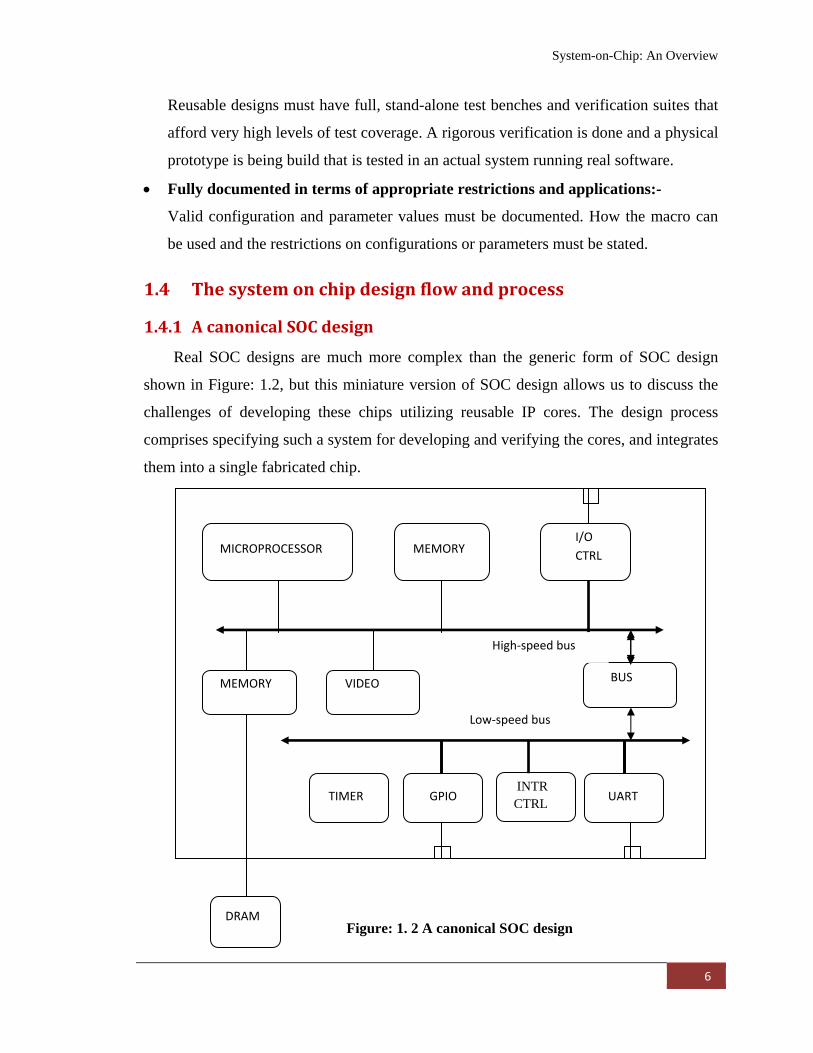
1.4.1 A canonical SOC design Real SOC designs are much more complex than the generic form of SOC design
shown in Figure: 1.2, but this miniature version of SOC design allows us to discuss the
challenges of developing these chips utilizing reusable IP cores. The design process
comprises specifying such a system for developing and verifying the cores, and integrates
them into a single fabricated chip.
Figure: 1. 2 A canonical SOC design
MICROPROCESSOR MEMORYI/O CTRL
MEMORY VIDEO BUS
TIMER GPIOINTR CTRL UART
DRAM
High‐speed bus
Low‐speed bus
System-on-Chip: An Overview
7
The above canonical SOC design contains the following blocks.
• A microprocessor may be 8 bit to 64 bit depending on the application.
• A memory module which may be single or multi-level and may include SRAM
and DRAM.
• An external memory controller for controlling flash or SRAM.
• A video decoder which may be MPEG or AVI.
• A I/O controller which may include PCI, Ethernet , USB, analog to digital, digital
to analog converter.
• A GPIO for general input output for interfacing external devices like LEDs or
LCDs or for sampling data.
1.4.2 System Design Flow A two major way of design flows are being used by design engineers in order to meet the
challenges of SOC design.
• From a waterfall model to a spiral model
• From a top-down methodology to a combinational of top-down and bottom-up
I. Waterfall vs. Spiral
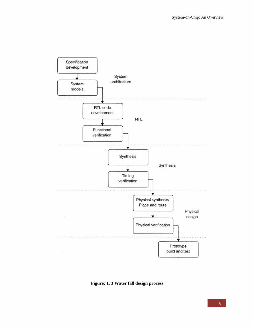
A traditional way of ASIC development, called waterfall model is shown in Figure:
1.3. In a waterfall model [2], the SOC design transits from phase to phase in a step, and
never returns to the activities of the previous phase. In this model, the design often tossed
“over the wall” from one team to the next with little interaction among them.
The phase of the design process starts with the development of a specification for
the ASIC. For complex ASIC the high algorithmic content is developed and given to the
design team to develop the RTL for the SOC. A set of verification is done in order to
ensure the proper functionality of the SOC design. After the complete verification, the
design is delivered to a team of synthesis experts to generate a gate level net list for the
hardware design of SOC. The proper functionality of the design is based on the timing
between the blocks of the design; a timing verification is performed to verify that the
ASIC meets timing.
System-on-Chip: An Overview
8
Figure: 1. 3 Water fall design process
System-on-Chip: An Overview
9
After timing is performed the design is given to the physical design team, which
places and routes the design. Finally, a prototype is built and tested. The prototype is
delivered to the software team for software debug. Software development is started
shortly after the hardware design is started.
This flow has worked well in designs of up to 100 k gates and down to 0.5 um [2].
A major demerit of this flow is the improper handoffs from one team to another. For
example the RTL design team may have to go back to the system designer and tell him
that the algorithm is not implementable, or the synthesis team may have to go back to the
RTL team and inform them that the RTL must be modified to meet the timing. As
complexity of system increases, geometry shrinks, and time to market pressures continue
to escalate, chip designers are turning to a modified flow to produce today’s larger SOC
designs. Hence design teams are moving from the old waterfall model to the newer spiral
development model, where the team works on multiple aspects of the design
simultaneously, incrementally improving in each area up to the completion of the design.
Figure: 1.4 shows the spiral SOC design flow [2] where designer addresses all aspects of
hardware and software design concurrently: functionality, timing, physical design and
verification.
• Concurrent development of hardware and software.
• Parallel verification and synthesis of modules.
• Floor planning and place-and-route included in the synthesis process.
• Modules developed only if a pre-designed hard and soft macro is not available.
• Planned iteration throughout.
II. Topdown Vs. Bottom up
The top down process begins with specification and decomposition, and ends with
integration and verification. These processes steps are describes as follows:-
1. Prepare a complete specification for the system and its subsystem.
2. Refine its algorithm and architecture, including software design and
hardware/software co-simulation if necessary.
3. Decompose the architecture into well -defined macros.
4. Design or select macros.
5. Integrate macros into the top level; verify functionality and timing.
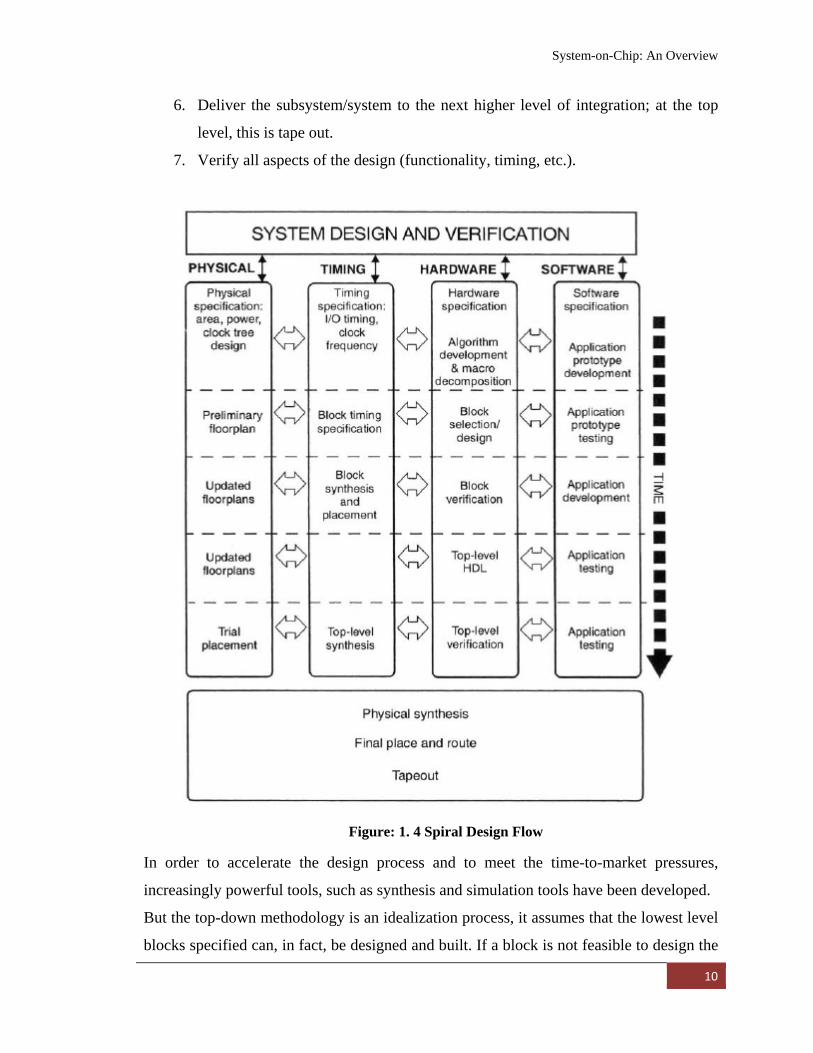
System-on-Chip: An Overview
10
6. Deliver the subsystem/system to the next higher level of integration; at the top
level, this is tape out.
7. Verify all aspects of the design (functionality, timing, etc.).
Figure: 1. 4 Spiral Design Flow
In order to accelerate the design process and to meet the time-to-market pressures,
increasingly powerful tools, such as synthesis and simulation tools have been developed.
But the top-down methodology is an idealization process, it assumes that the lowest level
blocks specified can, in fact, be designed and built. If a block is not feasible to design the
System-on-Chip: An Overview
11
whole specification process has to be repeated which increases the design time again. In
order to deal with this situation a mixture of top-down and bottom-up methodologies is
being used; where libraries of reusable hard and soft macros are used as a source of pre-
verified blocks; and it assures that at least some parts of the design can be designed and
fabricated in the target technology in order to meet the desired specification.
1.4.3 The System Design Process 1. Create the system specification
The design process begins with identifying the objectives of the design; such as system
requirements, the required functions, performance, and cost and development time for the
system. A set specification is recursively developed, verified and refined until they are
detailed enough to allow RTL coding to begin. Specification describes how to manipulate
the interfaces of a system to produce the desired behavior. Specifications are to be
provided for both hardware and software portions of the design. The following are the
specification requirements for the hardware and software portion of the design [2].
Hardware:
• functionality, external interfaces to other hardware (pins, buses and how to use
them)
• Interface to software (register definitions)
• Tiring and performance
• Area and power
Software:
• Functionality,
• Timing,
• Performance,
• Interface to hardware, software, structure and kernel.
These specifications are written jointly by engineering and marketing teams, in a natural
language, such as English. In order to avoid the ambiguities, incompleteness and errors,
companies have started using executable specifications for some or all of the system. An
executable specification is an abstract model for the hardware and software being used. It
System-on-Chip: An Overview
12
is written in C, C++ or SystemC or a Hardware verification language (HVL) for high
level specifications. At lower levels, hardware is usually described in Verilog or VHDL.
As executable specifications are only addressing the functional behavior of a system, so it
is necessary to describe critical physical specifications such as timing, clock frequency,
area and power requirements.
2. Develop a behavioral model
After specification is defined an initial high level of design is developed along with a
high-level behavioral model for the overall system. This model can be used to test the
basic algorithms of the system design and to show that meet the requirements outline in
the specification. For example, in an image and video processing design may need to
demonstrate that losses in compression/decompression are at or acceptable level. This
way of high-level model specification is termed as executable specification. These
specifications can be used as the reference for the future versions of the design.
3. Refine and test the behavioral models
After the behavioral model is defined in order to refine test algorithm a verification
environment for the high-level model is developed. This environment provides a
mechanism for refining the high-level design, verifying the functionality and
performance of the algorithm. This can be used later to verify models for the hardware
and software, such as RTL model verified using hardware/software simulation.
For example: - A multimedia or a graphics system may be initially coded in C/C++ with
all floating point operations. This allows the system architect to code and debug the basic
algorithm quickly. Once the algorithm is determined, a fixed-point version of the model
is developed that allows the architect to determine the accuracy level required in each
operation to achieve performance goals while minimizing die area.
Finally, a cycle-accurate and bit accurate model is developed, providing a very realistic
model for implementation. These multiple models are very useful for hardware/software
co-simulation to debug their software.
4. Determine the hardware/software partition
The hardware/software partition is the division of system functionality between hardware
and software. This is a manual process requiring judgment and experience on the part of
System-on-Chip: An Overview
13
the system architects and a good understanding of the cost/performance trade offs for
various architectures. A rich library of pre-verified, characterized macros and a rich
library of reusable software modules are the key things for identifying the size and
performance of various hardware and software functions. Finally, the interface between
the hardware and software is defined and the communication protocols between them are
also defined.
5. Specify and develop a hardware architectural model
Once the hardware requirements are defined, detail hardware architecture is specified.
The issues related to this are determining which hardware blocks will be used, and how
they will communicate, memory architecture, and bus structure and its bandwidth. Most
of the SOC communicates with different blocks over one or more bus, thus the required
bandwidth can be applicant dependent. A substantially amounts of application code is run
on the architecture to evaluate the bandwidth of the system. Running significant amounts
of application code on an RTL design is time consuming. In order to overcome this
problem, transaction-level models are developed to model interfaces and bus behavior.
This model can run considerably faster than RTL models and gives accurate estimates of
performance. SystemC is used to facilitate the design of transaction level modeling.
Finally, the hardware architecture is developed, tested and modified until a final
architecture meets the system requirements.
6. Refine and test the architectural model (co-simulation)
The software development often starts only once the hardware has been built. This
serialization may lead to delayed product. The architectural model for the system can be
used for hardware/software co-simulation. It provides sufficient accuracy that software
can be developed and debugged on it, long in advance of getting actual hardware. Hence
having accurate models of the hardware is the key issue in SOC design.
7. Specify implementation blocks
After the model is co-simulated hardware specification is provided which is a detailed
specification of the performance, functionality, and interfaces for the hardware system
and its component blocks. It also specify a description of the basic functions, the timing,
System-on-Chip: An Overview
14
area and the power requirements, and the physical and software interfaces and the
descriptions of the I/O pins and the register map.
1.5 System level Design Issues
This section discusses system level design issues such as different types of IP cores,
on chip buses, SOC test methodologies and SOC verification.
1.5.1 Different Types of IP Cores
I. Digital IP
In the previous section Design reuse is elaborated and we observed that well-
designed IP is the key to successful SOC design. The block used for SOC design must be
designed well unless, the tape out of the system becomes very painful and time-
consuming. Hence, well-designed IP core can be integrated with any SOC flow, and
produce good results quickly [2]. This section presents an issue related to produce well-
designed IP cores. The IP cores are classified into three categories [1]: Soft, firm and
hard.
Soft IP:
Soft IP blocks are specified in hardware description languages using RTL or
higher level descriptions. These are generally provided by the vendor in form of software
code which are process independent and can be synthesized to the gate level. Hence these
are more suitable for digital IP core design. These types of cores are sometimes not
guaranteed power or timing characteristics, as the implementation and application in
different process may produce variation in performance. But these types of IP cores are
very much flexible, portable and reusable and prevents the user frame introducing any
design errors into block. Hard IP:
Hard IP blocks have fixed layout and already go through physical design process.
This IPs is optimized for a given applicator in a specific process. As the timing
characteristics are optimized the performance of the IPs are predictable. The only
drawback is that, it requires additional effort and cost to produce this IPs. These are also
System-on-Chip: An Overview
15
limited to specific application but as this IPs are tested on Silicon the vendors gives more
assurance about its accuracy and correctness. Firm IP:
Firm IP are provided as parameterized circuit description so that designers can
optimize core for their specific design needs. Hence firm IPs are more predictable. These
are more flexible and portable than soft and hard IP.
Most of the digital processor blocks are being designed with hard IP in order to achieve
the performance goals. Memory cells are designed by transistor level and memory arrays
are tiled from these cells using a compiler [RMM]. Recently soft IP blocks preferred as
hand off level [1]. The typical soft IPs available is interface blocks (USB, UART, and
PCI), encryption blocks (DES, AES), multimedia blocks (JPEG, MPEG 2/4), and
networking blocks (ATM, Ethernet and Micro Controllers [1].
II. AMS IP
Another important IP which is gaining interest is Analog mixed signal IP. The
typical AMS components include operational amplifiers, analog to digital converters
(ADCs), digital to analog converters (DACs), phase locked loops (PLL), and radio
frequency (RF) modules etc. This IPs is designed using Hard IP and target to one
application in a specific fabrication technology.
1.5.2 System Interconnect and On ChipBuses In earlier days every chip designer had unique bus designed for optimum
performance for their own design project. This made difficult to reuse blocks from other
projects to their own designs. Hence, there was need of standard bus, which allows
reusable blocks developed with a single interface to be used for a variety of applications.
ARM [11] uses AMBA as system interconnects solution for their system design.
CoreConnect is being by IBM. The comparisons of three types of bus architecture are
presented in the Chapter-2 of the thesis.
1.5.3 SOC Test Methodologies Another important aspect of SOC integration is the development of a test
methodology for post manufacturing tests. Testing of SOC designs has many similarities
System-on-Chip: An Overview
16
with the traditional system on Board (SOB) designs. Cores in SOC are the components of
an SOC where as in printed circuit boards ICs are the components of SOB. In SOB, IC
design manufacturing and testing are performed by the IC provider and the system
integrator has to only design the board level designing using these ICs. In SOC, the core
providers supplies only the description of cores and the system integrator is responsible
to design any blocks called User Defined Logic (UDL), and integrates these predesigned
cores.
As the system is in logic level the system integrator cannot perform post
manufacturing test. Hence the integrator can only test the core logic wires between cores
and expects a set of test patterns with high fault coverage from the core provider. Another
key difference between the SOB and SOC is that unlike SOB the physical input output of
the cores are not accessible by the user in SOC. The test access to the embedded cores is
the responsibility of the system integrator. Hence additional logic and wiring,
mechanisms are required which leads to the development of core test access architecture
[1].
I. IP core level test
The testing of an IP core consists of an internal DFT Structures Design for Test
(DFT) structure and a required set of test patterns to be applied and captured on the core
periphery. The test pattern includes the data and protocol patterns. The data pattern
contains actual stimulus and response values. The protocol pattern specifies how to apply
and capture the test data. As the system integrator has very limited knowledge about the
structural content of the core, the core internal test should be carried at by the core
provider. Hence the core provider should provide the internal DFT hardware structure of
the core, the stimulus patterns of the core and the validation of these stimulus patterns.
The core provider must determine the internal core requirement of the core without
knowing the target process, application and the desired test coverage level. BIST is
another solution that can be used by core provider for core level testing.
System-on-Chip: An Overview
17
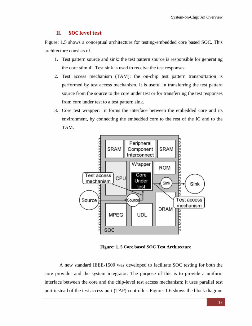
II. SOC level test
Figure: 1.5 shows a conceptual architecture for testing-embedded core based SOC. This
architecture consists of
1. Test pattern source and sink: the test pattern source is responsible for generating
the core stimuli. Test sink is used to receive the test responses.
2. Test access mechanism (TAM): the on-chip test pattern transportation is
performed by test access mechanism. It is useful in transferring the test pattern
source from the source to the core under test or for transferring the test responses
from core under test to a test pattern sink.
3. Core test wrapper: it forms the interface between the embedded core and its
environment, by connecting the embedded core to the rest of the IC and to the
TAM.
A new standard IEEE-1500 was developed to facilitate SOC testing for both the
core provider and the system integrator. The purpose of this is to provide a uniform
interface between the core and the chip-level test access mechanism; it uses parallel test
port instead of the test access port (TAP) controller. Figure: 1.6 shows the block diagram
Figure: 1. 5 Core based SOC Test Architecture
System-on-Chip: An Overview
18
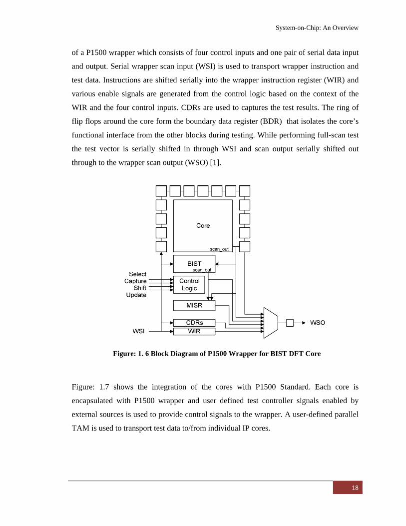
of a P1500 wrapper which consists of four control inputs and one pair of serial data input
and output. Serial wrapper scan input (WSI) is used to transport wrapper instruction and
test data. Instructions are shifted serially into the wrapper instruction register (WIR) and
various enable signals are generated from the control logic based on the context of the
WIR and the four control inputs. CDRs are used to captures the test results. The ring of
flip flops around the core form the boundary data register (BDR) that isolates the core’s
functional interface from the other blocks during testing. While performing full-scan test
the test vector is serially shifted in through WSI and scan output serially shifted out
through to the wrapper scan output (WSO) [1].
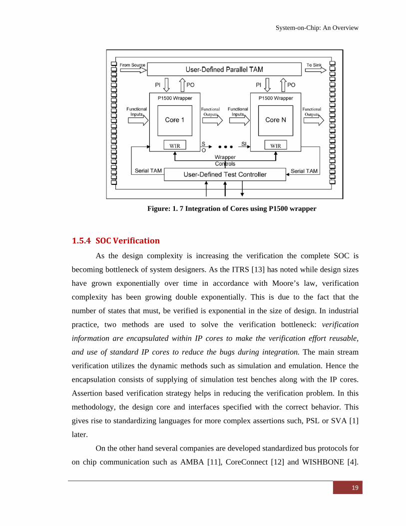
Figure: 1.7 shows the integration of the cores with P1500 Standard. Each core is
encapsulated with P1500 wrapper and user defined test controller signals enabled by
external sources is used to provide control signals to the wrapper. A user-defined parallel
TAM is used to transport test data to/from individual IP cores.
Figure: 1. 6 Block Diagram of P1500 Wrapper for BIST DFT Core
System-on-Chip: An Overview
19
1.5.4 SOC Verification As the design complexity is increasing the verification the complete SOC is
becoming bottleneck of system designers. As the ITRS [13] has noted while design sizes
have grown exponentially over time in accordance with Moore’s law, verification
complexity has been growing double exponentially. This is due to the fact that the
number of states that must, be verified is exponential in the size of design. In industrial
practice, two methods are used to solve the verification bottleneck: verification
information are encapsulated within IP cores to make the verification effort reusable,
and use of standard IP cores to reduce the bugs during integration. The main stream
verification utilizes the dynamic methods such as simulation and emulation. Hence the
encapsulation consists of supplying of simulation test benches along with the IP cores.
Assertion based verification strategy helps in reducing the verification problem. In this
methodology, the design core and interfaces specified with the correct behavior. This
gives rise to standardizing languages for more complex assertions such, PSL or SVA [1]
later.
On the other hand several companies are developed standardized bus protocols for
on chip communication such as AMBA [11], CoreConnect [12] and WISHBONE [4].
Figure: 1. 7 Integration of Cores using P1500 wrapper
System-on-Chip: An Overview
20
Adopting a standard interconnect not only eliminates the common errors occurring during
the design of an interconnection protocol, but also reduces the incorrect interfacing of
cores and interconnect. The above described methods help in reducing the verification
problems. But as the designed complexity increases the dynamic verification methods
suffers from poor verification coverage. Poor coverage increases the undetected bugs in
IP cores are undermine the goal of reusing IP cores without needing to completely re-
verify them.
Hence the formal verification methodology is used which minimizes the
probability of bugs in a design. More research activities focusing this area of verification.
The key research areas are compositional model checking. The specifications that are
verified and the assumption under which they are verified are documented and can be
exploited during integration verification. Again the methodology advancement in
dynamic verification helps in growing formal verification approach. Formal verification
is being used in many industry applications such as RTL gate-level equivalence checking
and microprocessor verification. Finally despite all the research advances now and in
future, it is impossible that the verification challenge can be solved without help from
designs. Leading companies involve verification experts early in the design process to
steer the design toward better verifiability [1].
1.6 Motivation
SOC design requires a standard bus interface for IP cores to communicate with each
other. There exist many other bus interfaces, but AMBA [11], CoreConnect [12] and
WISHBONE [4] are well known and well used SOC bus architectures. All three bus
architectures are open bus architectures, which require no fees or royalties to use them.
WISHBONE offers advantage compared to AMBA and CoreConnect. All designer using
WISHBONE bus interface are allowed to upload their design in Open Core site where there
exists many IP cores that support WISHBONE bus interface and they are all free to use. So
depending upon the design specification the designer can select the IP cores from the site
and glue them to the WISHBONE bus architecture to design the final SOC. Comparing the
architecture of these three buses, it is observed that all are supported by multiplexer
interconnections. WISHBONE supports variable interconnection and variable time
System-on-Chip: An Overview
21
specification. It can be coded using any hardware description language like VHDL and
Verilog®, and it takes the shapes of simple logic gates supported by most of the FPGA
and ASIC devices. WISHBONE also supports Single and Block Read/Write cycles, Read-
Modify-Write (RMW) transfer. In respect to all of the above issues WISHBONE
supports almost all features also supported by AMBA and CoreConnect. It also offers
advantage of using predesigned IP cores available freely Open Core site for the portable
and reliable SOC design. Keeping in view of the above, in this dissertation we adopt
WISHBONE for SOC design and explore the Open Core based SOC design platform.
1.7 Work Presented in the Thesis The major contributions of this thesis are:
• The possibility of using an existing bus interface for faster and low cost SoC
design is evaluated. The design, verification, FPGA implementation of
WISHBONE interconnection architectures in terms of size and speed for SoC
design is evaluated.
• A set of wishbone compatible cores such as 32-bit RISC CPU, on chip memory,
universal asynchronous receiver and transmitter (UART), Parallel Input Output
(PIO) and System controller (SYS) are collected from Open Core and integrated
to develop a portable low cost SoC design.
• The integration issues are discussed and the synthesis results in terms of size and
speed are presented. A test bench is developed in order to verify the CPU
instruction with the final integrated architecture.
• Finally, FPGA implementation of SoC architecture has been done using
VIRTEX-II Pro FPGA and the functionality of the system is verified through
porting the application software on the SoC architecture.
1.8 Thesis Outline
The layout of this thesis compiled is as follows:
Chapter 1: The first chapter presents introduction to SOC design. This chapter also
discusses SOC design process and system level issues such as design of reusable IP core,
System-on-Chip: An Overview
22
on chip bus interface and strategies for synthesis, verification and testing. A brief
overview of the thesis outline is presented here.
Chapter 2: The second chapter describes the concept of Open Hardware. The Open Core
based SOC design platform is illustrated. The design reuse using Wishbone bus
specification is also presented in this chapter.
Chapter 3: In this chapter Design and verification of a point-to-point interconnection and
shared bus interconnection using DMA MASTER and memory SLAVE core is presented.
The bench marking of the interconnections in terms of size and speed is evaluated by
using two FPGA technologies.
Chapter 4: This chapter presents a description of design methodology to implement
proposed SOC Architecture in FPGA using Wishbone bus interface. The design
specifications of the IP cores are described here.
Chapter 5: SOC integration issues and verification results, synthesis and FPGA
implementation of the SOC architecture is presented in this chapter.
Chapter 6: This chapter demonstrates the validation of SOC architecture with porting
application software developed in GNU C compiler and debugger.
Chapter 7: Finally, a conclusion is drawn in this last chapter. This chapter also lists the
future research scopes from the studies undertaken.
1.9 Conclusions
The concept of SOC design through design reuse is discussed, and the design flow
and design process steps are described. The various issues related to system level design
are addressed and observed that
• Design Reuse through well design IP cores is the key factor behind reliable time
to market SOC design.
• A standard interface bus must be adopted to get reduced integration efforts.
• The design of test circuits must be done properly in during the SOC integration to
avoid post manufacturing physical error.
• A proper verification methodology must be adopted to validate the final
functionality of the SOC.
23
Platform Based SOC Design Open Core Based SOC Design Platform The Objective behind WISHBONE WISHBONE Basics WISHBONE Interface Specification Wishbone Interconnections WISHBONE Bus Cycle Data Organization and Customized Tag WISHBONE SOC Bus Comparison with AMBA and CoreConnect
Conclusions
Chapter 2
Open Core Based SOC Design Platform
Open Core Based SOC Design Platform
24
SOC design increases the density of transistor in a chip. The increased density of
transistor in turn increases the complexity of the system. The SOC design methodology
offers definite benefits; however there are certain challenges like larger design space,
higher design and prototype costs, high level of debugging methodology, power
management, and longer design and prototyping cycle time. Apart from these challenges,
the design again needs an expertise in both hardware and software levels for proper
hardware and software co-design. Another important aspect of SOC integration is the
development of a proper test methodology for post manufacturing test. All these
integration issues makes the design time consuming and also expensive.
To deal with this inherent integration problems and reduction in design cycle
time, many methods for SOC design are proposed by research and industry community.
There are several methods for SOC design, however in this thesis we limit our discussion
for two methods of SOC design. These are Platform based SOC design and Open Core
SOC design methodology. This chapter also explains about the features of Open Core on
chip bus interface WISHBONE which is the key factor in Open core SOC design
methodology. Finally, different bus interfaces available for SOC design have been
compared.
2.1 Platform Based SOC Design In Platform based design (PBD), new designs could be quickly created from the
original platform over many design derivatives. More specifically a platform is an
abstraction level that covers a number of refinements to a lower level resulting in
improvement of the design productivity. An SOC platform consists of hardware IP,
software IP, programmable IP, standardized bus structures and communication networks,
computer-aided design (CAD) flows for hardware/software design, verification and
implementation, system validation tools, design derivative creation tools and dedicated
hardware for system prototyping [1]. PBD is a design methodology which starts at system
level and high productivity is achieved by using predictable, pre-verified blocks that uses
standard interfaces.
The two major areas in PBD methodology are (a) block authoring and (b) system-
chip integration [15]. Block authoring uses a methodology which creates block that
Open Core Based SOC Design Platform
25
interfaces easily with multiple target designs. Two design concepts used in block
authoring are interfacing standardization and virtual system design.
In interfacing standardization, both internal and external design teams can do
block authoring, as long as they are using the same design methodology and the same
interface specifications. The interface standard used can be product or application
specific.
In virtual system design, the designer has to focus about the power profile,
clocking schemes, internal clock distribution, and testing schemes of the design. Also
block interfaces (with a single bus or multiple bus) types, and the type of block such as
soft, hard or firm are also decided during virtual system design.
System chip integration focuses on designing and verifying the system
architecture and the interfaces between the blocks. Integration process starts with
partitioning the system around the pre-existing block level functions and identifying the
new or differentiating function needed. These partitioning are done at the system level,
along with performance analysis, hardware /software design trade-offs, and functional
verification.
The benefits of PBD are as follows:
• Design uses diverse and specialized functions from multiple sources. Hence
planned design reuse yields very high productivity.
• Hierarchical routing and timing reduce design focus.
• Interface based design promotes and multiple reuse for blocks allows amortization
of development cost and more optimal block design.
The challenges of PBD include:
• Planned reuse requires proper design planning and accurate future product plans.
• Significant software portions require extensive hardware/software co-verification.
• Platform migration to new process technology requires re-characterization of
hard, soft IPs and platform architecture.
• Requires organizational change to support separate block authoring and system
chip integration.
Hence, PBD can be treated as a convergence design where previously separated
functions are integrated. The pre-existing blocks can be accurately estimated and the
Open Core Based SOC Design Platform
26
design variability limited to the new blocks and the interface architecture. It requires
organizational support to create a PBD.
2.2 Open Core Based SOC Design Platform On the other hand, a new concept that is gaining interest is the Open Core SOC
design methodology which publishes all necessary information about the hardware [3].
This is termed as open hardware. All the information regarding the hardware is disclosed
for free, according to the term of GPL/LGPL license. Open Core [4] group has provided
many pre-synthesized and pre-verified hardware core for the designer. These cores are
well documented with design specifications, RTL codes, and simulation test benches and
therefore can be re-used for different applications. Making a design compatible with an
on-chip bus interface is one way to produce re-usable design. Different IP cores
developed independently can be tied together and tested by standardizing the IP core
interfaces. Many re-usable digital designs available in the Open Core site are compatible
with a standard on-chip interface called WISHBONE [5] bus interface. More than 800
projects are available in open core site. Some of them are Open RISC1200 processor,
VGA controller, USB 2.0, memory controller, UART, MAC, PCI and many DSP
functionality cores. The designer has to collect the IP cores from the site and integrate it
into the design to complete the SOC design. All these cores are available at no cost and
are reusable. Hence it helps in producing low cost, portable, reliable, time-to-market SOC
design. The EDA tools used to develop open hardware are also open. Hence in Open
Core SOC design methodology openness of resources is a key factor to develop design
reuse and improve the productivity of SOC designs.
2.3 The Objective behind WISHBONE The WISHBONE System-on-Chip (SOC) Interconnection is a method for
connecting IP cores together to form integrated circuits. Open core SOC design
methodology utilizes WISHBONE bus interface to foster design reuse by alleviating
system-on-chip integration problems. With use of this standardize bus interface it is much
easier to connect the cores, and therefore much easier to create a custom System-on-Chip.
This way of SOC design improves the portability and reliability of the system, and results
in faster time-to-market for the end user. The objective behind WISHBONE is to create a
Open Core Based SOC Design Platform
27
portable interface that supports both FPGA and ASIC that is independent of the
semiconductor technology and WISHBONE interfaces should be independent of logic
signaling levels. Another important reason is to create a flexible interconnection scheme
that is independent of the type of IP core delivery (Hard, Soft IP) method. The next
reasons are to have a standard interface that can be written using any hardware
description language such as VHDL and VERILOG®. It supports a variety of bus
transfer cycle in which the data transaction is independent of the application specific
functions of the IP cores. It also supports different types of interconnection architectures
with theoretically infinite range of operating frequency [5]. The final objective of
WISHBONE bus is that it is absolutely free to use by developers without paying any fee
for the cores available.
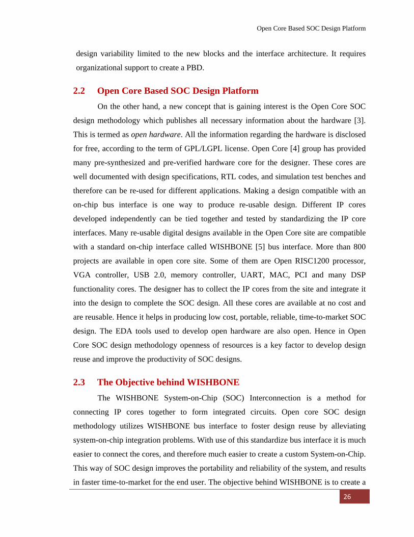
2.4 WISHBONE Basics WISHBONE utilizes “Master” and “Slave” architectures which are connected to
each other through an interface called “Intercon”. Master is an IP core that initiates the
data transaction to the SLAVE IP core.
Master starts transaction providing an address and control signal to Slave. Slave
in turn responds to the data transaction with the Master with the specified address range.
Figure: 2. 1 WISHBONE Intercon system
Open Core Based SOC Design Platform
28
The Intercon is the medium consists of wires and logics which help in data transfer
between Master and Slave. The Intercon also requires a “SYSCON” module which
generates WISHBONE reset and clock signal for the proper functioning of the system.
Figure: 2.1 show the WISHBONE Intercon system which consists of Masters and Slaves
and SYSCON modules. WISHBONE Intercon can be designed to operate over an infinite
frequency range. This is called as variable time specification. The speed of the operation
is only limited by the technology of the integrated circuits. The interconnection can be
described using hardware description languages like VHDL and Verilog®, and the
system integrator can modify the interconnection according to the requirement of the
design. Hence WISHBONE interface is different from traditional microcomputer buses
such as PCI, VME bus and ISA bus.
2.5 WISHBONE Interface Specification WISHBONE Interface specification specifies the signaling method used by
Master and Slave interface and the SYSCON module. It also specifies the way to create a
proper documentation for the WISHBONE Compatible IP cores which is the main
driving factor for design reuse.
2.5.1 Documentation for IP Cores As specified above each WISHBONE Compatible IP cores must be supplied with
a WISHBONE datasheet, which describes the interface of the cores. This datasheet helps
in understanding the operation of the cores, and the user can reuse these cores to integrate
with other cores to produce System on a Chip. The WISHBONE datasheet must include
the following information:
• The revision level of the WISHBONE specification after which it is designed.
• If the IP designed is a Master or Slave IP core.
• The signal names used in the design must be defined. If any signal name different
than that defined in the specification, must have a cross reference to the original
signal of the specification.
• If a Master supports a retry and error signal, then it must specify how they react in
response to the signals. If a Slave supports retry and error signal, then it must
specify under which conditions the signal must be generated.
Open Core Based SOC Design Platform
29
• The design supporting tag signals must specify the name, TAG TYPE and
operation of the tag.
• The port size must be 8-bit, 16-bit, 32-bit or 64-bit.
• The maximum operand size used must be 8-bit, 16-bit, 32-bit or 64-bit.
• The data transfer ordering such as LITTLE ENDIAN or BIG ENDIAN must be
specified.
• Any constraints on the clock signal [CLK_I] must be specified in terms of clock
frequency, application specific timing constraints, use of gated clocks or use of
variable clock generators.
2.5.2 WISHBONE Interface Signal
WISHBONE interface signals and bus cycles are design in a reusable manner, so
that the WISHBONE Master and Slave interfaces can be connected together using several
interconnection methods. These signals are classified into three categories, Master
signals, Slave signals, and signals common to both Masters and Slaves. These entire
interface signals must be active high logic.
The signal definitions must follow these requirements:
• The signal must allow Master and Slave to use variable interconnections.
• The signals must support all the basic types of bus cycle.
• A handshaking mechanism must be used for either the Master or the participating
Slave interface to adjust the data transfer rate.
• Every interface must support acknowledgement signal but the retry and error
acknowledgement signals are optional.
• Address and data bus widths can be altered to fit different applications like 8-bit,
16-bit, 32-bit and 64-bit data buses.
• All the signals should be either output or input. The signals may be bidirectional,
if the target device supports it.
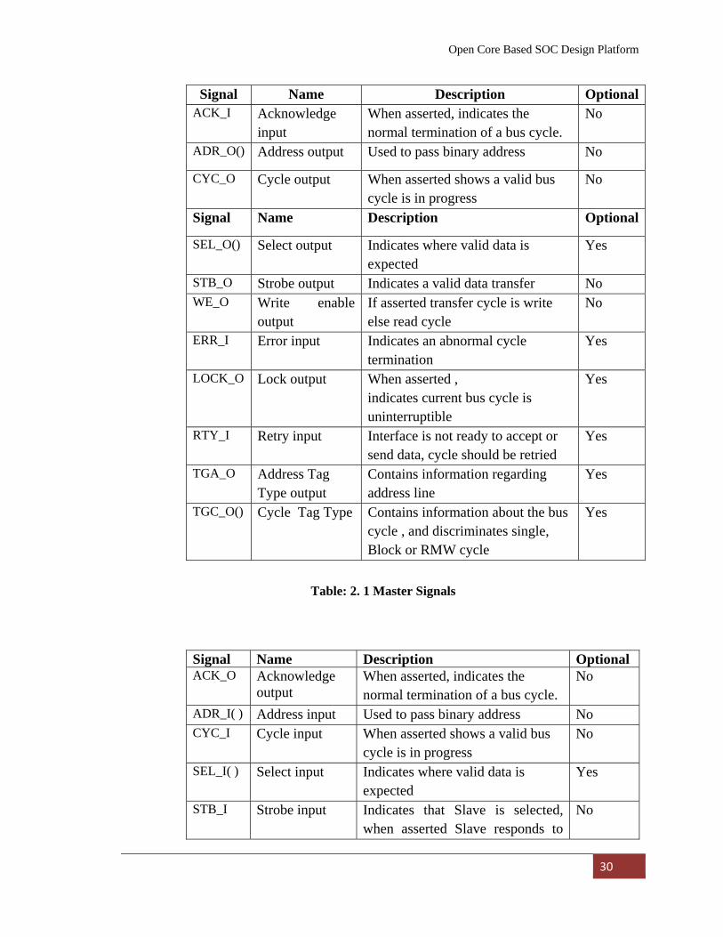
The Tables: 2.1, 2.2 and 2.3 below show the descriptions of these three types of signals.
The optional requirement of the signal is also specified in the table.
Open Core Based SOC Design Platform
30
Signal Name Description OptionalACK_I Acknowledge
input When asserted, indicates the normal termination of a bus cycle.
No
ADR_O() Address output Used to pass binary address No
CYC_O Cycle output When asserted shows a valid bus cycle is in progress
No
Signal Name Description Optional
SEL_O() Select output Indicates where valid data is expected
Yes
STB_O Strobe output Indicates a valid data transfer No WE_O Write enable
output If asserted transfer cycle is write else read cycle
No
ERR_I Error input Indicates an abnormal cycle termination
Yes
LOCK_O Lock output When asserted , indicates current bus cycle is uninterruptible
Yes
RTY_I Retry input Interface is not ready to accept or send data, cycle should be retried
Yes
TGA_O Address Tag Type output
Contains information regarding address line
Yes
TGC_O() Cycle Tag Type Contains information about the bus cycle , and discriminates single, Block or RMW cycle
Yes
Table: 2. 1 Master Signals
Signal Name Description Optional ACK_O Acknowledge
output When asserted, indicates the normal termination of a bus cycle.
No
ADR_I( ) Address input Used to pass binary address No CYC_I Cycle input When asserted shows a valid bus
cycle is in progress No
SEL_I( ) Select input Indicates where valid data is expected
Yes
STB_I Strobe input Indicates that Slave is selected, when asserted Slave responds to
No
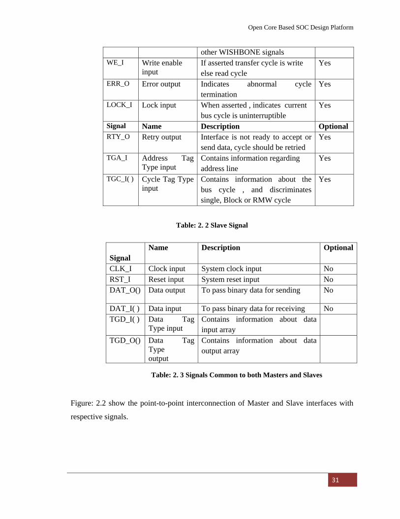
Open Core Based SOC Design Platform
31
other WISHBONE signals WE_I Write enable
input If asserted transfer cycle is write else read cycle
Yes
ERR_O Error output Indicates abnormal cycle termination
Yes
LOCK_I Lock input When asserted , indicates current bus cycle is uninterruptible
Yes
Signal Name Description Optional RTY_O Retry output Interface is not ready to accept or
send data, cycle should be retried Yes
TGA_I Address Tag Type input
Contains information regarding address line
Yes
TGC_I( ) Cycle Tag Type input
Contains information about the bus cycle , and discriminates single, Block or RMW cycle
Yes
Table: 2. 2 Slave Signal
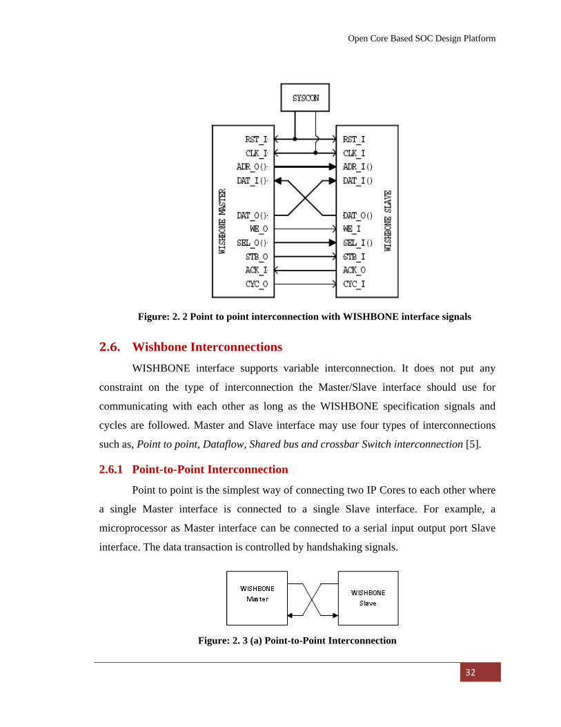
Figure: 2.2 show the point-to-point interconnection of Master and Slave interfaces with
respective signals.
Signal
Name Description Optional
CLK_I Clock input System clock input No RST_I Reset input System reset input No DAT_O()
Data output To pass binary data for sending No
DAT_I( ) Data input To pass binary data for receiving No TGD_I( )
Data Tag Type input
Contains information about data input array
TGD_O()
Data Tag Type output
Contains information about data output array
Table: 2. 3 Signals Common to both Masters and Slaves
Open Core Based SOC Design Platform
32
2.6. Wishbone Interconnections WISHBONE interface supports variable interconnection. It does not put any
constraint on the type of interconnection the Master/Slave interface should use for
communicating with each other as long as the WISHBONE specification signals and
cycles are followed. Master and Slave interface may use four types of interconnections
such as, Point to point, Dataflow, Shared bus and crossbar Switch interconnection [5].
2.6.1 Point-to-Point Interconnection
Point to point is the simplest way of connecting two IP Cores to each other where
a single Master interface is connected to a single Slave interface. For example, a
microprocessor as Master interface can be connected to a serial input output port Slave
interface. The data transaction is controlled by handshaking signals.
Figure: 2. 3 (a) Point-to-Point Interconnection
Figure: 2. 2 Point to point interconnection with WISHBONE interface signals
Open Core Based SOC Design Platform
33
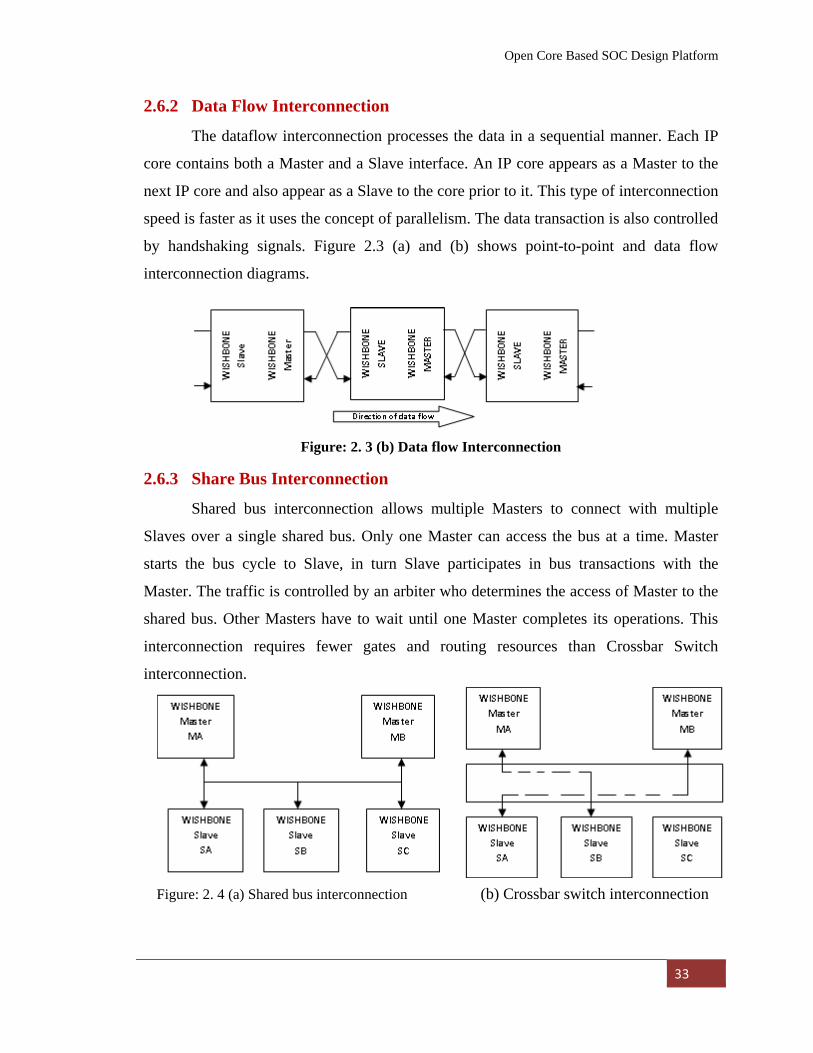
2.6.2 Data Flow Interconnection
The dataflow interconnection processes the data in a sequential manner. Each IP
core contains both a Master and a Slave interface. An IP core appears as a Master to the
next IP core and also appear as a Slave to the core prior to it. This type of interconnection
speed is faster as it uses the concept of parallelism. The data transaction is also controlled
by handshaking signals. Figure 2.3 (a) and (b) shows point-to-point and data flow
interconnection diagrams.
Figure: 2. 3 (b) Data flow Interconnection
2.6.3 Share Bus Interconnection
Shared bus interconnection allows multiple Masters to connect with multiple
Slaves over a single shared bus. Only one Master can access the bus at a time. Master
starts the bus cycle to Slave, in turn Slave participates in bus transactions with the
Master. The traffic is controlled by an arbiter who determines the access of Master to the
shared bus. Other Masters have to wait until one Master completes its operations. This
interconnection requires fewer gates and routing resources than Crossbar Switch
interconnection.
Figure: 2. 4 (a) Shared bus interconnection (b) Crossbar switch interconnection
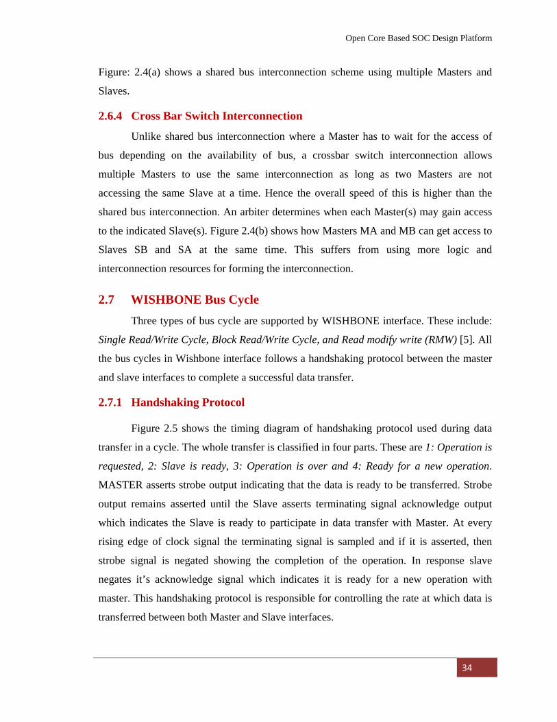
Open Core Based SOC Design Platform
34
Figure: 2.4(a) shows a shared bus interconnection scheme using multiple Masters and
Slaves.
2.6.4 Cross Bar Switch Interconnection
Unlike shared bus interconnection where a Master has to wait for the access of
bus depending on the availability of bus, a crossbar switch interconnection allows
multiple Masters to use the same interconnection as long as two Masters are not
accessing the same Slave at a time. Hence the overall speed of this is higher than the
shared bus interconnection. An arbiter determines when each Master(s) may gain access
to the indicated Slave(s). Figure 2.4(b) shows how Masters MA and MB can get access to
Slaves SB and SA at the same time. This suffers from using more logic and
interconnection resources for forming the interconnection.
2.7 WISHBONE Bus Cycle
Three types of bus cycle are supported by WISHBONE interface. These include:
Single Read/Write Cycle, Block Read/Write Cycle, and Read modify write (RMW) [5]. All
the bus cycles in Wishbone interface follows a handshaking protocol between the master
and slave interfaces to complete a successful data transfer.
2.7.1 Handshaking Protocol
Figure 2.5 shows the timing diagram of handshaking protocol used during data
transfer in a cycle. The whole transfer is classified in four parts. These are 1: Operation is
requested, 2: Slave is ready, 3: Operation is over and 4: Ready for a new operation.
MASTER asserts strobe output indicating that the data is ready to be transferred. Strobe
output remains asserted until the Slave asserts terminating signal acknowledge output
which indicates the Slave is ready to participate in data transfer with Master. At every
rising edge of clock signal the terminating signal is sampled and if it is asserted, then
strobe signal is negated showing the completion of the operation. In response slave
negates it’s acknowledge signal which indicates it is ready for a new operation with
master. This handshaking protocol is responsible for controlling the rate at which data is
transferred between both Master and Slave interfaces.
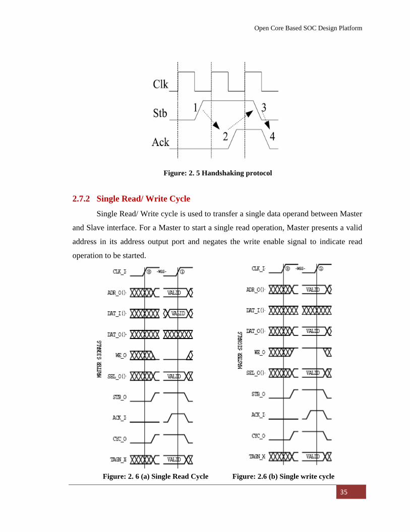
Open Core Based SOC Design Platform
35
2.7.2 Single Read/ Write Cycle
Single Read/ Write cycle is used to transfer a single data operand between Master
and Slave interface. For a Master to start a single read operation, Master presents a valid
address in its address output port and negates the write enable signal to indicate read
operation to be started.
Figure: 2. 5 Handshaking protocol
Figure: 2. 6 (a) Single Read Cycle Figure: 2.6 (b) Single write cycle
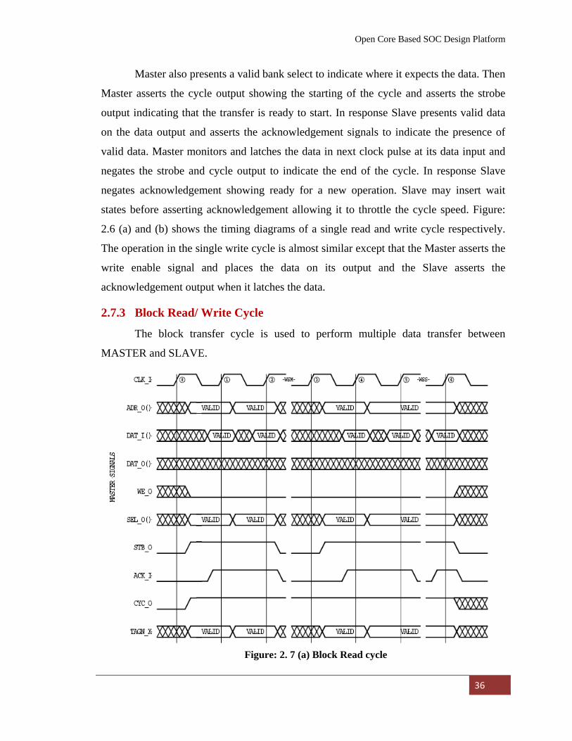
Open Core Based SOC Design Platform
36
Master also presents a valid bank select to indicate where it expects the data. Then
Master asserts the cycle output showing the starting of the cycle and asserts the strobe
output indicating that the transfer is ready to start. In response Slave presents valid data
on the data output and asserts the acknowledgement signals to indicate the presence of
valid data. Master monitors and latches the data in next clock pulse at its data input and
negates the strobe and cycle output to indicate the end of the cycle. In response Slave
negates acknowledgement showing ready for a new operation. Slave may insert wait
states before asserting acknowledgement allowing it to throttle the cycle speed. Figure:
2.6 (a) and (b) shows the timing diagrams of a single read and write cycle respectively.
The operation in the single write cycle is almost similar except that the Master asserts the
write enable signal and places the data on its output and the Slave asserts the
acknowledgement output when it latches the data.
2.7.3 Block Read/ Write Cycle
The block transfer cycle is used to perform multiple data transfer between
MASTER and SLAVE.
Figure: 2. 7 (a) Block Read cycle
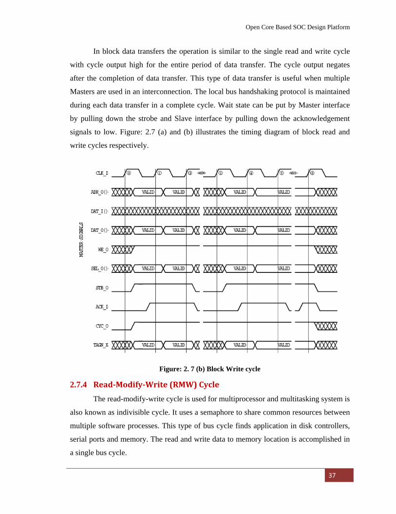
Open Core Based SOC Design Platform
37
In block data transfers the operation is similar to the single read and write cycle
with cycle output high for the entire period of data transfer. The cycle output negates
after the completion of data transfer. This type of data transfer is useful when multiple
Masters are used in an interconnection. The local bus handshaking protocol is maintained
during each data transfer in a complete cycle. Wait state can be put by Master interface
by pulling down the strobe and Slave interface by pulling down the acknowledgement
signals to low. Figure: 2.7 (a) and (b) illustrates the timing diagram of block read and
write cycles respectively.
Figure: 2. 7 (b) Block Write cycle
2.7.4 ReadModifyWrite (RMW) Cycle
The read-modify-write cycle is used for multiprocessor and multitasking system is
also known as indivisible cycle. It uses a semaphore to share common resources between
multiple software processes. This type of bus cycle finds application in disk controllers,
serial ports and memory. The read and write data to memory location is accomplished in
a single bus cycle.
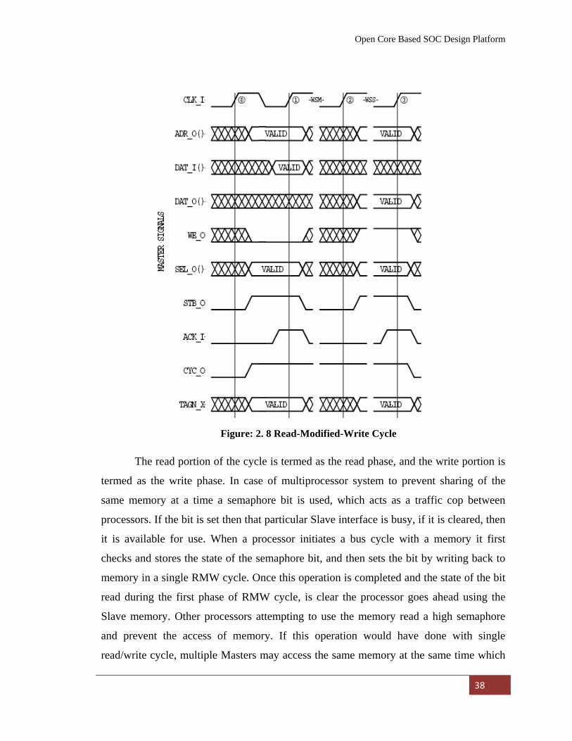
Open Core Based SOC Design Platform
38
The read portion of the cycle is termed as the read phase, and the write portion is
termed as the write phase. In case of multiprocessor system to prevent sharing of the
same memory at a time a semaphore bit is used, which acts as a traffic cop between
processors. If the bit is set then that particular Slave interface is busy, if it is cleared, then
it is available for use. When a processor initiates a bus cycle with a memory it first
checks and stores the state of the semaphore bit, and then sets the bit by writing back to
memory in a single RMW cycle. Once this operation is completed and the state of the bit
read during the first phase of RMW cycle, is clear the processor goes ahead using the
Slave memory. Other processors attempting to use the memory read a high semaphore
and prevent the access of memory. If this operation would have done with single
read/write cycle, multiple Masters may access the same memory at the same time which
Figure: 2. 8 Read-Modified-Write Cycle
Open Core Based SOC Design Platform
39
may lead to system crash. A special instruction such as test-and-set (TAS) and compare-
and-set (CAS) are used by processors to impose RMW bus cycle operation. Figure: 2.8
show the timing diagram of RMW cycle.
2.8 Data Organization and Customized Tag WISHBONE interface supports two ways of ordering of data during data transfer.
These are BIG ENDIAN and LITTLE ENDIAN. In the first type the most significant
byte of the operand placed at the higher address and in the second type, the most
significant byte of an operand placed at the lower address.
The advantage of WISHBONE interface over traditional computer buses is that
WISHBONE can be customized easily. WISHBONE interconnections are programmable
in FPGA and ASIC by using VHDL and Verilog® languages and wide variety of routing
tools. Although it allows changes in interconnection; still there may be a chance of
interface incompatibility. This problem can be avoided by using tagged architecture.
There are three categories of TAG TYPE available. They are address tag, cycle tag and a
set of data tag [5]. Custom tags can be added to WISHBONE interface signals with the
TAG TYPE available. The tag indicates the exact time of the signal response.
2.9 WISHBONE SOC Bus Comparison with AMBA and CoreConnect SOC design requires a standard bus interface for IP cores to communicate with each
other. There exist many other bus interfaces, but AMBA, CoreConnect and WISHBONE are
well known and well used SOC bus architectures, therefore here the comparison is restricted
to these buses. All three bus architectures are open bus architectures, which require no fees or
royalties to use them. AMBA and CoreConnect require registration to get a free license to use.
WISHBONE on the other hand doesn't require any kind of registration. The WISHBONE
specification is almost free to copy and distribute. SOC design using AMBA and
CoreConnect requires the designer to design their own library of IP cores or to buy IP cores
from other companies. WISHBONE offers advantage compared to AMBA and CoreConnect.
All designer using WISHBONE bus interface are allowed to upload their design in Open Core
site where there exists many IP cores that support WISHBONE bus interface and they are all
free to use. So depending upon the design specification the designer can select the IP cores
from the site and glue them to the WISHBONE bus architecture to design the final SOC.
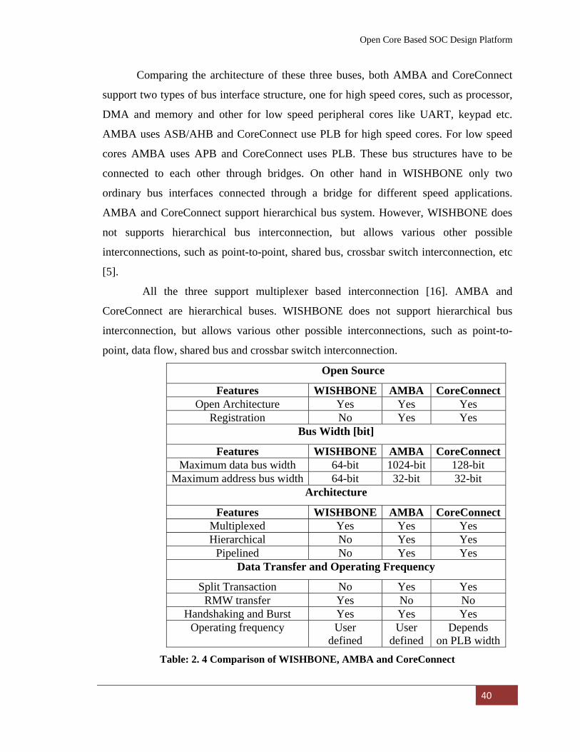
Open Core Based SOC Design Platform
40
Comparing the architecture of these three buses, both AMBA and CoreConnect
support two types of bus interface structure, one for high speed cores, such as processor,
DMA and memory and other for low speed peripheral cores like UART, keypad etc.
AMBA uses ASB/AHB and CoreConnect use PLB for high speed cores. For low speed
cores AMBA uses APB and CoreConnect uses PLB. These bus structures have to be
connected to each other through bridges. On other hand in WISHBONE only two
ordinary bus interfaces connected through a bridge for different speed applications.
AMBA and CoreConnect support hierarchical bus system. However, WISHBONE does
not supports hierarchical bus interconnection, but allows various other possible
interconnections, such as point-to-point, shared bus, crossbar switch interconnection, etc
[5].
All the three support multiplexer based interconnection [16]. AMBA and
CoreConnect are hierarchical buses. WISHBONE does not support hierarchical bus
interconnection, but allows various other possible interconnections, such as point-to-
point, data flow, shared bus and crossbar switch interconnection.
Open Source
Features WISHBONE AMBA CoreConnectOpen Architecture Yes Yes Yes
Registration No Yes Yes Bus Width [bit]
Features WISHBONE AMBA CoreConnectMaximum data bus width 64-bit 1024-bit 128-bit
Maximum address bus width 64-bit 32-bit 32-bit Architecture
Features WISHBONE AMBA CoreConnectMultiplexed Yes Yes Yes Hierarchical No Yes Yes
Pipelined No Yes Yes Data Transfer and Operating Frequency
Split Transaction No Yes Yes RMW transfer Yes No No
Handshaking and Burst Yes Yes Yes Operating frequency User
defined User
defined Depends
on PLB widthTable: 2. 4 Comparison of WISHBONE, AMBA and CoreConnect
Open Core Based SOC Design Platform
41
AMBA and CoreConnect both support split transfer in which a Slave has the
possibility to release the bus to other Masters requesting it and having a higher priority
than the Master using it. However WISHBONE supports Read-Modify-Write (RMW)
transfer. In a multiprocessor system in order to avoid two or more Masters gaining access
to the same Slave the Master has to use a RMW cycle.
RMW cycle gives a Master the opportunity to do both a read and a write
operation before any other Master may use the bus and thereby avoiding a system crash.
The operating frequency of AMBA and WISHBONE are user defined but the
CoreConnect operating frequency is decided by the data width of PLB [17].
In respect to all of the above issues WISHBONE supports almost all features also
supported by AMBA and CoreConnect. It also offers advantage of using predesigned IP
cores available freely in Open Core site for the portable and reliable SOC design.
Keeping view this features we adopt the WISHBONE interface for our SOC design. A
summary of all the features of these three buses are given in Table 2.4.
2.10 Conclusions As design complexity increases, many SOC design methodologies have been
proposed by research and industry community [3]. Some of them are still in development
phase. Platform based SOC design is an emerging technology that utilizes previously
design platform of abstraction level to form SOC design. But it requires a library of
platform which can only possible in industry environment. On the other hand Open Core
design offers SOC design using design reuse with a standard bus interface. WISHBONE
bus interface made By Silicore [18] Corporation is a solution to the necessity of a
standard bus interface. Open core utilizes WISHBONE interface for design reuse and
help in plug and play integration of freely available IP cores that leads to low cost,
reliable, time-to-market SOC design. The features of WISHBONE specification such as
documentation, signal naming, types of interconnections and bus cycles has been
discussed. Finally a comparison of WISHBONE bus with other two industry standard bus
interface AMBA and CoreConnect has been done.
Open Core Based SOC Design Platform
42
The brief summary of Wishbone bus interface with compared to other standards in
industry are given below:
• Standard interfaces are available freely and can be used for SOC integration in
industry as well as laboratory environment without any additional cost.
• It supports single Read/Write; block Read/Write bus cycles. It also supports
RMW cycle as compared to split transaction of AMBA and CoreConnect to share
same memory being used in multiprocessor SOC environment.
• The interconnection scheme supports variable interconnection and variable time
specification. That means it can be changed by the system integrator and can be
operated at any frequency which is limited to the technology of the target device.
• The edge of Wishbone interconnection over other microcomputer buses like PCI,
VME bus is that it can be coded using any hardware description language like
VHDL and Verilog®, and it takes the shapes of simple logic gates supported by
most of the FPGA and ASIC devices.
Design and Verifications of WISHBONE Interconnections
43
DESIGN AND VERIFICATION OF WISHBONE INTERCONNECTIONS
Design of WISHBONE Compatible Slave
IP Core
Point‐to‐Point Interconnection
Shared Bus Interconnection
Conclusions
Chapter 3
Design and Verifications of WISHBONE Interconnections
44
After the WISHBONE interface features have been discussed, the next step is to
create a WISHBONE compatible Slave core. For this purpose a 16-bit Slave output port
core has been taken and the issues related to make it WISHBONE compatible are
specified. The corresponding simulation results of the core using Xilinx ISE simulator is
provided. This chapter also demonstrates the design and verification of two types of bus
interconnections such as point to point and shared bus interconnections. The various
related issues to create the interconnection are also presented here. A bench marking of
these two portable systems has been done to determine the maximum speed and
minimum size in two types of FPGAs. The system consists of 32-bit DMA with Master
interface which transfers data to and from 32-bit MEMORY with Slave interface. The
verification results using Xilinx [20] ISE simulator and ChipScope Pro results are
provided to validate the functionality of the system.
3.1 Design of WISHBONE Compatible Slave IP Core
This section describes how to make a WISHBONE Compatible Slave IP core, so
that user designed IP cores can be used in integration process for designing SOC. The
idea behind this section is to demonstrate how WISHBONE interfaces work in
conjunction with logic primitives available on FPGA and ASIC devices. It also
demonstrates that a very little logic is needed to implement WISHBONE interface.
3.1.1 16-Bit Slave Output Port Design with 8-Bit Granularity
Figure: 3.1 shows a simple 16-bit WISHBONE Slave output port with 8-bit granularity,
which means that data can be transferred 8 or 16-bits at a time. The issues related to
making this core WISHBONE compatible are listed below:
1. To perform the write operation on Slave the data presented in the data input of Slave
DATI (15:0) is latched in synchronous with the rising edge of clock signal CLK_I
when strobe, select signal and write enable are asserted. The data input port to Slave
consists of 16-bit data of 8-bit granularity. This means that the 16-bit register can be
accessed with either 8 or 16-bit bus cycles.
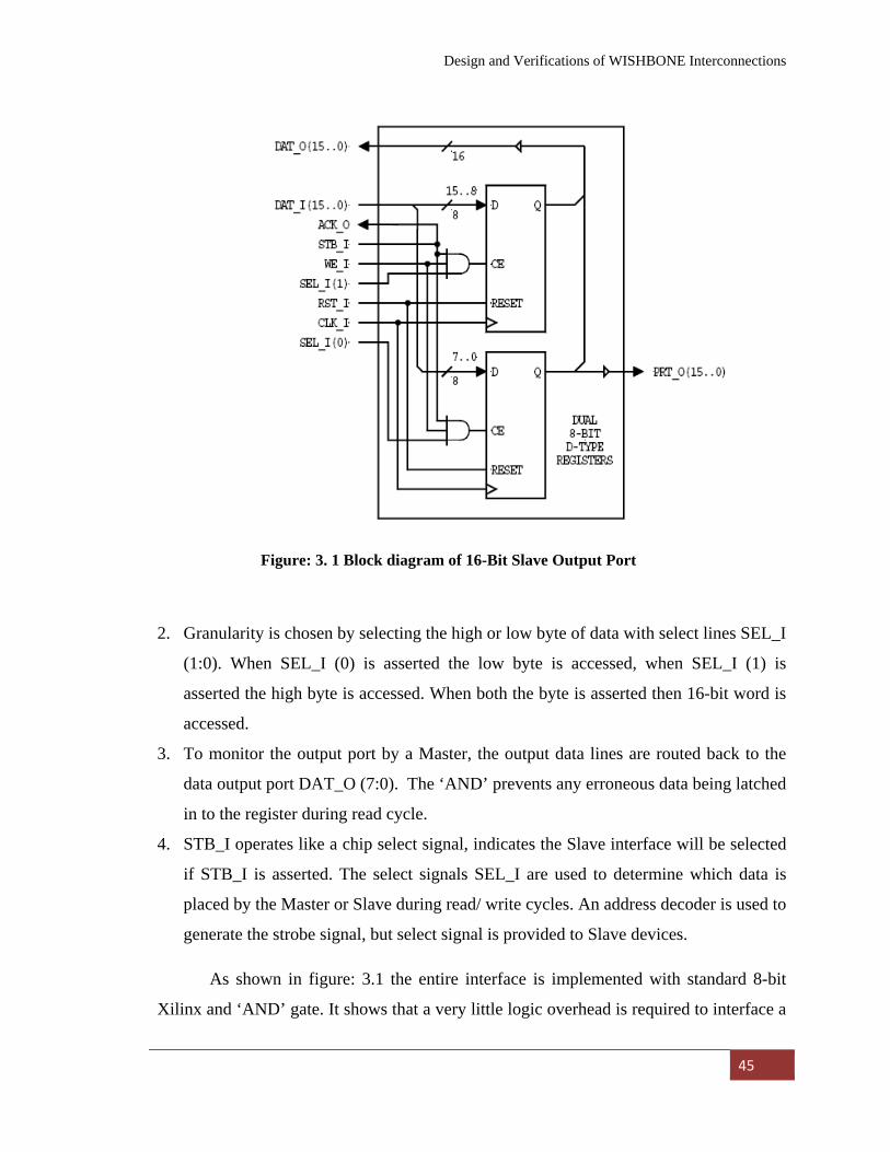
Design and Verifications of WISHBONE Interconnections
45
2. Granularity is chosen by selecting the high or low byte of data with select lines SEL_I
(1:0). When SEL_I (0) is asserted the low byte is accessed, when SEL_I (1) is
asserted the high byte is accessed. When both the byte is asserted then 16-bit word is
accessed.
3. To monitor the output port by a Master, the output data lines are routed back to the
data output port DAT_O (7:0). The ‘AND’ prevents any erroneous data being latched
in to the register during read cycle.
4. STB_I operates like a chip select signal, indicates the Slave interface will be selected
if STB_I is asserted. The select signals SEL_I are used to determine which data is
placed by the Master or Slave during read/ write cycles. An address decoder is used to
generate the strobe signal, but select signal is provided to Slave devices.
As shown in figure: 3.1 the entire interface is implemented with standard 8-bit
Xilinx and ‘AND’ gate. It shows that a very little logic overhead is required to interface a
Figure: 3. 1 Block diagram of 16-Bit Slave Output Port
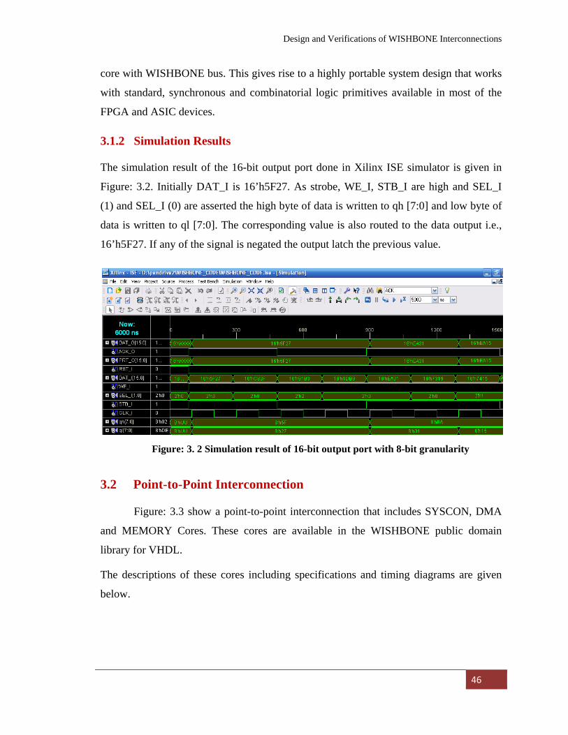
Design and Verifications of WISHBONE Interconnections
46
core with WISHBONE bus. This gives rise to a highly portable system design that works
with standard, synchronous and combinatorial logic primitives available in most of the
FPGA and ASIC devices.
3.1.2 Simulation Results
The simulation result of the 16-bit output port done in Xilinx ISE simulator is given in
Figure: 3.2. Initially DAT_I is 16’h5F27. As strobe, WE_I, STB_I are high and SEL_I
(1) and SEL_I (0) are asserted the high byte of data is written to qh [7:0] and low byte of
data is written to ql [7:0]. The corresponding value is also routed to the data output i.e.,
16’h5F27. If any of the signal is negated the output latch the previous value.
3.2 Point-to-Point Interconnection
Figure: 3.3 show a point-to-point interconnection that includes SYSCON, DMA
and MEMORY Cores. These cores are available in the WISHBONE public domain
library for VHDL.
The descriptions of these cores including specifications and timing diagrams are given
below.
Figure: 3. 2 Simulation result of 16-bit output port with 8-bit granularity
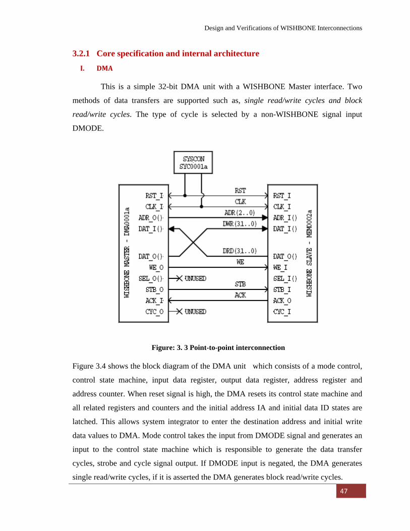
Design and Verifications of WISHBONE Interconnections
47
3.2.1 Core specification and internal architecture
I. DMA
This is a simple 32-bit DMA unit with a WISHBONE Master interface. Two
methods of data transfers are supported such as, single read/write cycles and block
read/write cycles. The type of cycle is selected by a non-WISHBONE signal input
DMODE.
Figure 3.4 shows the block diagram of the DMA unit which consists of a mode control,
control state machine, input data register, output data register, address register and
address counter. When reset signal is high, the DMA resets its control state machine and
all related registers and counters and the initial address IA and initial data ID states are
latched. This allows system integrator to enter the destination address and initial write
data values to DMA. Mode control takes the input from DMODE signal and generates an
input to the control state machine which is responsible to generate the data transfer
cycles, strobe and cycle signal output. If DMODE input is negated, the DMA generates
single read/write cycles, if it is asserted the DMA generates block read/write cycles.
Figure: 3. 3 Point-to-point interconnection
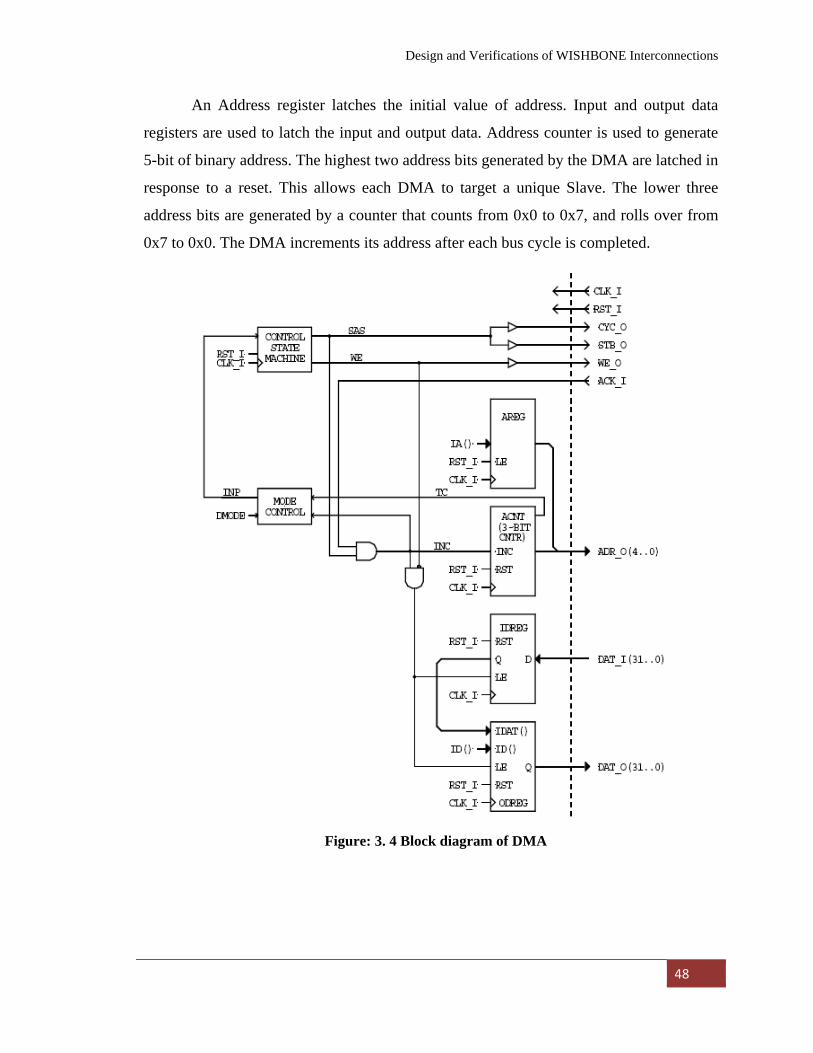
Design and Verifications of WISHBONE Interconnections
48
An Address register latches the initial value of address. Input and output data
registers are used to latch the input and output data. Address counter is used to generate
5-bit of binary address. The highest two address bits generated by the DMA are latched in
response to a reset. This allows each DMA to target a unique Slave. The lower three
address bits are generated by a counter that counts from 0x0 to 0x7, and rolls over from
0x7 to 0x0. The DMA increments its address after each bus cycle is completed.
Figure: 3. 4 Block diagram of DMA
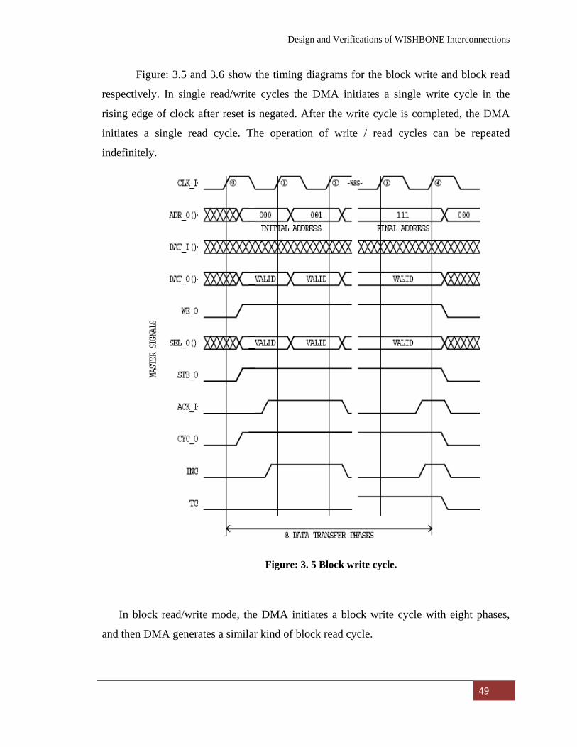
Design and Verifications of WISHBONE Interconnections
49
Figure: 3.5 and 3.6 show the timing diagrams for the block write and block read
respectively. In single read/write cycles the DMA initiates a single write cycle in the
rising edge of clock after reset is negated. After the write cycle is completed, the DMA
initiates a single read cycle. The operation of write / read cycles can be repeated
indefinitely.
In block read/write mode, the DMA initiates a block write cycle with eight phases,
and then DMA generates a similar kind of block read cycle.
Figure: 3. 5 Block write cycle.
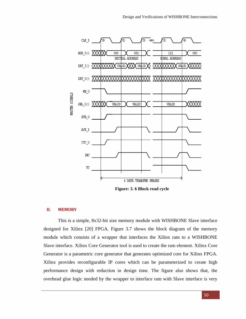
Design and Verifications of WISHBONE Interconnections
50
II. MEMORY
This is a simple, 8x32-bit size memory module with WISHBONE Slave interface
designed for Xilinx [20] FPGA. Figure 3.7 shows the block diagram of the memory
module which consists of a wrapper that interfaces the Xilinx ram to a WISHBONE
Slave interface. Xilinx Core Generator tool is used to create the ram element. Xilinx Core
Generator is a parametric core generator that generates optimized core for Xilinx FPGA.
Xilinx provides reconfigurable IP cores which can be parameterized to create high
performance design with reduction in design time. The figure also shows that, the
overhead glue logic needed by the wrapper to interface ram with Slave interface is very
Figure: 3. 6 Block read cycle
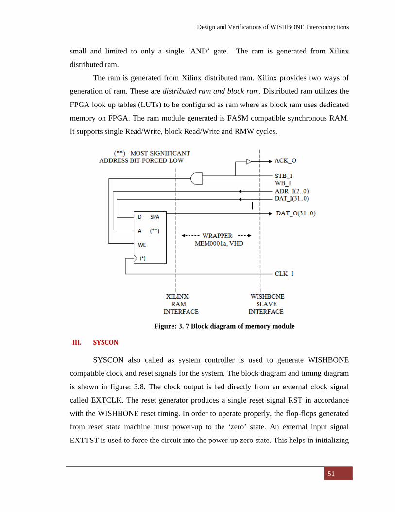
Design and Verifications of WISHBONE Interconnections
51
small and limited to only a single ‘AND’ gate. The ram is generated from Xilinx
distributed ram.
The ram is generated from Xilinx distributed ram. Xilinx provides two ways of
generation of ram. These are distributed ram and block ram. Distributed ram utilizes the
FPGA look up tables (LUTs) to be configured as ram where as block ram uses dedicated
memory on FPGA. The ram module generated is FASM compatible synchronous RAM.
It supports single Read/Write, block Read/Write and RMW cycles.
III. SYSCON
SYSCON also called as system controller is used to generate WISHBONE
compatible clock and reset signals for the system. The block diagram and timing diagram
is shown in figure: 3.8. The clock output is fed directly from an external clock signal
called EXTCLK. The reset generator produces a single reset signal RST in accordance
with the WISHBONE reset timing. In order to operate properly, the flop-flops generated
from reset state machine must power-up to the ‘zero’ state. An external input signal
EXTTST is used to force the circuit into the power-up zero state. This helps in initializing
Figure: 3. 7 Block diagram of memory module
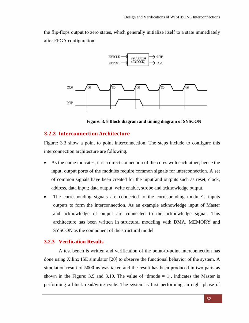
Design and Verifications of WISHBONE Interconnections
52
the flip-flops output to zero states, which generally initialize itself to a state immediately
after FPGA configuration.
3.2.2 Interconnection Architecture Figure: 3.3 show a point to point interconnection. The steps include to configure this
interconnection architecture are following.
• As the name indicates, it is a direct connection of the cores with each other; hence the
input, output ports of the modules require common signals for interconnection. A set
of common signals have been created for the input and outputs such as reset, clock,
address, data input; data output, write enable, strobe and acknowledge output.
• The corresponding signals are connected to the corresponding module’s inputs
outputs to form the interconnection. As an example acknowledge input of Master
and acknowledge of output are connected to the acknowledge signal. This
architecture has been written in structural modeling with DMA, MEMORY and
SYSCON as the component of the structural model.
3.2.3 Verification Results
A test bench is written and verification of the point-to-point interconnection has
done using Xilinx ISE simulator [20] to observe the functional behavior of the system. A
simulation result of 5000 ns was taken and the result has been produced in two parts as
shown in the Figure: 3.9 and 3.10. The value of ‘dmode = 1’, indicates the Master is
performing a block read/write cycle. The system is first performing an eight phase of
Figure: 3. 8 Block diagram and timing diagram of SYSCON
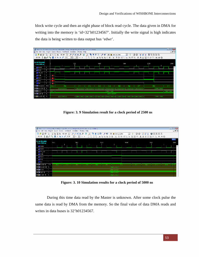
Design and Verifications of WISHBONE Interconnections
53
block write cycle and then an eight phase of block read cycle. The data given in DMA for
writing into the memory is ‘id=32’h01234567’. Initially the write signal is high indicates
the data is being written to data output bus ‘edwr’.
During this time data read by the Master is unknown. After some clock pulse the
same data is read by DMA from the memory. So the final value of data DMA reads and
writes in data buses is 32’h01234567.
Figure: 3. 9 Simulation result for a clock period of 2500 ns
Figure: 3. 10 Simulation results for a clock period of 5000 ns
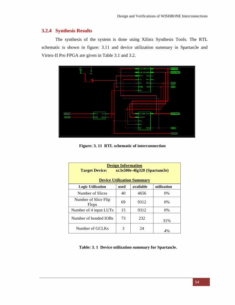
Design and Verifications of WISHBONE Interconnections
54
3.2.4 Synthesis Results
The synthesis of the system is done using Xilinx Synthesis Tools. The RTL
schematic is shown in figure: 3.11 and device utilization summary in Spartan3e and
Virtex-II Pro FPGA are given in Table 3.1 and 3.2.
Design Information Target Device: xc3s500e-4fg320 (Spartam3e)
Device Utilization Summary
Logic Utilization used available utilization
Number of Slices 40 4656 0% Number of Slice Flip
Flops 69 9312 0%
Number of 4 input LUTs 15 9312 0%
Number of bonded IOBs 73 232 31%
Number of GCLKs 3 24 4%
Table: 3. 1 Device utilization summary for Spartan3e.
Figure: 3. 11 RTL schematic of interconnection
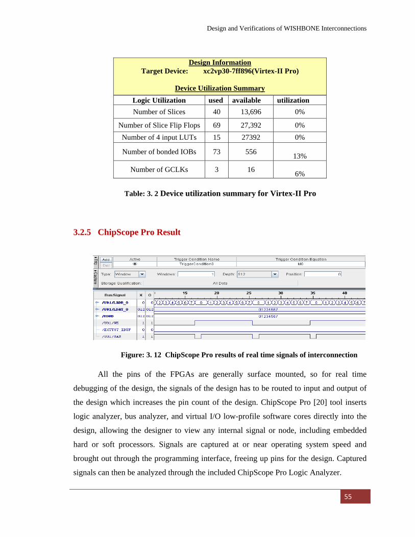
Design and Verifications of WISHBONE Interconnections
55
3.2.5 ChipScope Pro Result
All the pins of the FPGAs are generally surface mounted, so for real time
debugging of the design, the signals of the design has to be routed to input and output of
the design which increases the pin count of the design. ChipScope Pro [20] tool inserts
logic analyzer, bus analyzer, and virtual I/O low-profile software cores directly into the
design, allowing the designer to view any internal signal or node, including embedded
hard or soft processors. Signals are captured at or near operating system speed and
brought out through the programming interface, freeing up pins for the design. Captured
signals can then be analyzed through the included ChipScope Pro Logic Analyzer.
Design Information Target Device: xc2vp30-7ff896(Virtex-II Pro)
Device Utilization Summary
Logic Utilization used available utilization Number of Slices 40 13,696 0%
Number of Slice Flip Flops 69 27,392 0% Number of 4 input LUTs 15 27392 0%
Number of bonded IOBs 73 556 13%
Number of GCLKs 3 16 6%
Table: 3. 2 Device utilization summary for Virtex-II Pro
Figure: 3. 12 ChipScope Pro results of real time signals of interconnection
Design and Verifications of WISHBONE Interconnections
56
Figure: 3.12 shows the real time debugging of internal signals through Xilinx
ChipScope Pro tool. EDRD and LDAT_0 are the date read and data write bus signals
which shows that the DMA is reading and writing 32’h01234567 to and from the
memory module. SAS and WE are the strobe and write enable signals of the system. The
figure also demonstrates that the system is performing eight phases of write cycle and
then eight phases of read cycles successfully.
3.2.6 Benchmarking Results
For benchmarking purpose synthesis results from two types of Xilinx FPGAs
have been taken such as, Spartan-3e and Virtex-II Pro and compared. Here benchmarking
indicates determining the maximum speed with the minimum area occupied by the
interconnection in two types of FPGA technology. The tables shows 40 no.s of slices are
required to form the interconnection in both the two types of FPGAs. The maximum
speed of the interconnection in Spartan3e and Virtex-II Pro are 248.675 MHz and
450.113 MHz respectively.
Table 3.2
32 bit Point-to-Point interconnection benchmark results
MFG & Type Part Number Size Max Speed
Xilinx Spartan3e XC3S500e-4fg320 40 slices 248.675 MHz
Xilinx Virtex-II Pro Xc2vp30 -7ff896 40 slices 450.113 MHz
Table: 3. 3 32-bit Point-to-Point interconnection benchmark results
3.3. Shared Bus Interconnection
This section describes the SOC design using shared bus interconnection. A 32-bit
shared bus system is created which consists of four Masters and four Slaves. The
modules used in point-to-point interconnection such as DMA, MEMORY and SYSCON
has been used to form the interconnection and to explore the various integration issues
related to shared bus interconnection. SOC design using shared bus interconnection is
more complex than the point-to-point interconnection scheme. It imposes some of the

Design and Verifications of WISHBONE Interconnections
57
design complexities to the system integrator during SOC integration. System integrator
has to perform some task before the final SOC integration.
These tasks include:
1. The type of bus topology i.e., multiplexed and non-multiplexed bus.
2. The type of interconnection logic i.e., three-state and multiplexor based
interconnection logic.
3. Arbiters are required to grant bus access to the Master. The integrator has to
decide which type of arbiter should be chosen depending on the application.
4. An address map should be created, so that Master can access the Slave through its
binary address value using variable address decoding.
5. Creating the topology for interconnection.
All these issues are discussed and final benchmarking of the system in terms of
minimum size and maximum speed has been presented in this section.
3.3.1. Bus topology
The important thing in designing a system is to how to move the data around the system.
The data may be a binary address value or a simple data value.
Hence buses are used to move the data around a system. There may be a chance
that two different buses are required for data and address transfer or in a single bus data
and address may be multiplexed to reduce the number of interconnections.
Two types of bus topology exists
I. Multiplexed, bus topology and
II. Non-multiplexed bus topology.
In multiplexed bus different types of data are routed over the same bus signals. Hence the
number of interconnections require in multiplexed bus topology are less. Figure: 3.13
show a multiplexed bus where 32 bit address and 32 bit data are being presented in the
same bus; this reduces the number of signals in interconnection from 64 to 32.
This bus topology is used in semiconductor industry to reduce the number of pins
on a chip. The major disadvantages of the multiplexed bus topology are that it requires
two clock pulses to move the data and address information in a system. Hence where
speed is concerned a non-multiplexed synchronous bus is used to move the data and
address information in a single clock cycle. It requires more interconnection logic as data
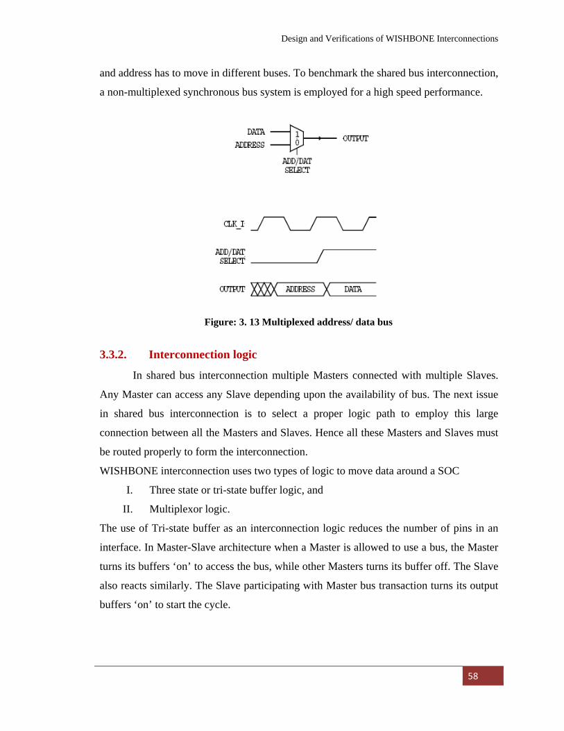
Design and Verifications of WISHBONE Interconnections
58
and address has to move in different buses. To benchmark the shared bus interconnection,
a non-multiplexed synchronous bus system is employed for a high speed performance.
3.3.2. Interconnection logic
In shared bus interconnection multiple Masters connected with multiple Slaves.
Any Master can access any Slave depending upon the availability of bus. The next issue
in shared bus interconnection is to select a proper logic path to employ this large
connection between all the Masters and Slaves. Hence all these Masters and Slaves must
be routed properly to form the interconnection.
WISHBONE interconnection uses two types of logic to move data around a SOC
I. Three state or tri-state buffer logic, and
II. Multiplexor logic.
The use of Tri-state buffer as an interconnection logic reduces the number of pins in an
interface. In Master-Slave architecture when a Master is allowed to use a bus, the Master
turns its buffers ‘on’ to access the bus, while other Masters turns its buffer off. The Slave
also reacts similarly. The Slave participating with Master bus transaction turns its output
buffers ‘on’ to start the cycle.
Figure: 3. 13 Multiplexed address/ data bus
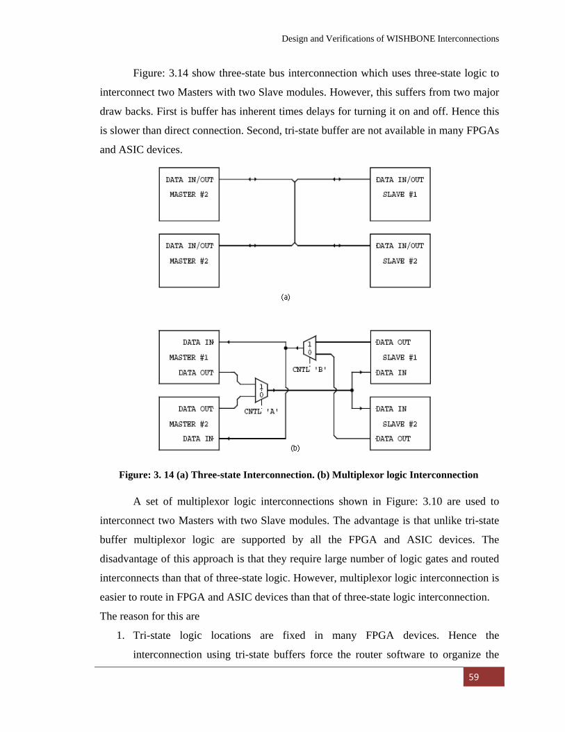
Design and Verifications of WISHBONE Interconnections
59
Figure: 3.14 show three-state bus interconnection which uses three-state logic to
interconnect two Masters with two Slave modules. However, this suffers from two major
draw backs. First is buffer has inherent times delays for turning it on and off. Hence this
is slower than direct connection. Second, tri-state buffer are not available in many FPGAs
and ASIC devices.
A set of multiplexor logic interconnections shown in Figure: 3.10 are used to
interconnect two Masters with two Slave modules. The advantage is that unlike tri-state
buffer multiplexor logic are supported by all the FPGA and ASIC devices. The
disadvantage of this approach is that they require large number of logic gates and routed
interconnects than that of three-state logic. However, multiplexor logic interconnection is
easier to route in FPGA and ASIC devices than that of three-state logic interconnection.
The reason for this are
1. Tri-state logic locations are fixed in many FPGA devices. Hence the
interconnection using tri-state buffers force the router software to organize the
Figure: 3. 14 (a) Three-state Interconnection. (b) Multiplexor logic Interconnection
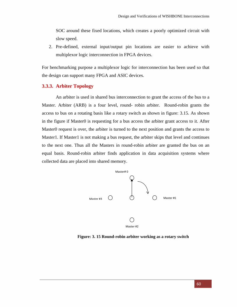
Design and Verifications of WISHBONE Interconnections
60
SOC around these fixed locations, which creates a poorly optimized circuit with
slow speed.
2. Pre-defined, external input/output pin locations are easier to achieve with
multiplexor logic interconnection in FPGA devices.
For benchmarking purpose a multiplexor logic for interconnection has been used so that
the design can support many FPGA and ASIC devices.
3.3.3. Arbiter Topology
An arbiter is used in shared bus interconnection to grant the access of the bus to a
Master. Arbiter (ARB) is a four level, round- robin arbiter. Round-robin grants the
access to bus on a rotating basis like a rotary switch as shown in figure: 3.15. As shown
in the figure if Master0 is requesting for a bus access the arbiter grant access to it. After
Master0 request is over, the arbiter is turned to the next position and grants the access to
Master1. If Master1 is not making a bus request, the arbiter skips that level and continues
to the next one. Thus all the Masters in round-robin arbiter are granted the bus on an
equal basis. Round-robin arbiter finds application in data acquisition systems where
collected data are placed into shared memory.
Figure: 3. 15 Round-robin arbiter working as a rotary switch
Master #1
Master# 0
Master #3
Master #2
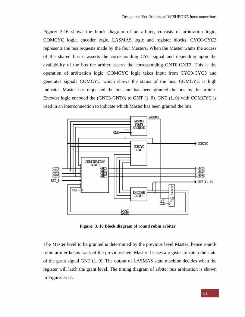
Design and Verifications of WISHBONE Interconnections
61
Figure: 3.16 shows the block diagram of an arbiter, consists of arbitration logic,
COMCYC logic, encoder logic, LASMAS logic and register blocks. CYC0-CYC3
represents the bus requests made by the four Masters. When the Master wants the access
of the shared bus it asserts the corresponding CYC signal and depending upon the
availability of the bus the arbiter asserts the corresponding GNT0-GNT3. This is the
operation of arbitration logic. COMCYC logic takes input from CYC0-CYC3 and
generates signals COMCYC which shows the status of the bus. COMCYC is high
indicates Master has requested the bus and has been granted the bus by the arbiter.
Encoder logic encoded the (GNT3-GNT0) to GNT (1..0). GNT (1..0) with COMCYC is
used in an interconnection to indicate which Master has been granted the bus.
The Master level to be granted is determined by the previous level Master; hence round-
robin arbiter keeps track of the previous level Master. It uses a register to catch the state
of the grant signal GNT (1..0). The output of LASMAS state machine decides when the
register will latch the grant level. The timing diagram of arbiter bus arbitration is shown
in Figure: 3.17.
Figure: 3. 16 Block diagram of round robin arbiter
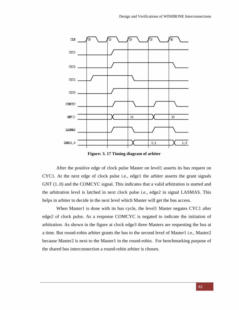
Design and Verifications of WISHBONE Interconnections
62
After the positive edge of clock pulse Master on level1 asserts its bus request on
CYC1. At the next edge of clock pulse i.e., edge1 the arbiter asserts the grant signals
GNT (1..0) and the COMCYC signal. This indicates that a valid arbitration is started and
the arbitration level is latched in next clock pulse i.e., edge2 in signal LASMAS. This
helps in arbiter to decide in the next level which Master will get the bus access.
When Master1 is done with its bus cycle, the level1 Master negates CYC1 after
edge2 of clock pulse. As a response COMCYC is negated to indicate the initiation of
arbitration. As shown in the figure at clock edge3 three Masters are requesting the bus at
a time. But round-robin arbiter grants the bus to the second level of Master1 i.e., Master2
because Master2 is next to the Master1 in the round-robin. For benchmarking purpose of
the shared bus interconnection a round-robin arbiter is chosen.
Figure: 3. 17 Timing diagram of arbiter
Design and Verifications of WISHBONE Interconnections
63
3.3.4. Partial address decoding and address map
Every Slave in an interconnection is defined by a specific binary address. In order
to access the Slave the Master has to decode the corresponding address. Two types of
methods are used to decode the address in a system. These are,
I. Full address decoding, and
II. Partial address decoding.
Most of the standard microcomputer buses like PCI and VME bus use full address
decoding. In this type decoding of full address of the bus is utilized to access a Slave. i.e.,
if a 32it address is used, then each Slave will be assigned with all thirty two address bits.
In partial decoding a range of the address is assigned as a decoding address of the Slave
module. In other way, if the Slave has four registers, then WISHBONE interface utilizes
only to address bits for decoding the Slave. Standard microcomputer buses the
interconnection method cannot be changed, so it uses a full address for decoding,
whereas WISHBONE supports variable interconnection and allows partial decoding
method.
The partial decoding method has the following advantages:
• As part of an address is in use, the size of the decoder is minimized and it allows
high speed decoders and speeds up the interface.
• It requires less redundant decoding logic or gates.
• It supports variable sizing. i.e., in WISHBONE the address path can be of any
size between 0 and 64-bits.
• It supports variable interconnection scheme.
As WISHBONE is using partial decoding technique, the integrator has flexibility in
defining the address map of the system. However, partial decoding technique suffers
from a disadvantage that the SOC integrator has to define address decoder logic for each
IP core, which increases the effort of integrating cores into the SOC. Table: 3.4 shows the
address map used in designing the shared bus interconnection.
Design and Verifications of WISHBONE Interconnections
64
Table 3.3 Address map used by Interconnection
DMA Master Memory SLAVE Address Cycles
Master0 Slave0 0x00 – 0x07 Block Read/Write
Master1 Slave1 0x08 – 0x0F Block Read/write
Master2 Slave2 0x10 – 0x17 Block Read/Write
Master3 Slave3 0x18 – 0x1F Block Read/Write
Table: 3. 4 Address map used by Interconnection
3.3.5. Interconnection topology
A shared bus interconnection is created for benchmarking purpose with a
multiplexor interconnections and non-multiplexed address and data buses. Figure: 3.18
shows the block diagram of general share bus interconnection for n number of Master and
Slaves. For system design four DMA Master and four Memory Slave modules. A
SYSCON module is used to provide the system with clock and reset signal. An arbiter
module is taken to grant the access of the bus to Masters.
The steps for creating this interconnection architecture are as follows:
1) A top module file is created where four DMAs, four memory modules are
instantiated as components in a structural model. The output of the DMA such as
ADR_O, DAT_O, SEL_O, WE_O, STB_O, is routed to five multiplexors
respectively. The outputs of the multiplexors form the corresponding bus to carry
the data from the DMAs. This is how multiplexor logic interconnection has been
created. Similar bus interconnection is created for data input DAT_I.
2) An address comparator is used to decode the address values so that Master can
access the corresponding Slaves from the decoded address.
The operation of interconnection is described below:
1) After the initial system reset, one or more Masters request the interconnection or bus
by asserting their cycle output signal CYC_O. Arbiter grants the bus to one of the
Design and Verifications of WISHBONE Interconnections
65
Figure: 3. 18 Block Diagram of a Generalised Shared bus Interconnection
Design and Verifications of WISHBONE Interconnections
66
2) Masters requesting for bus, after one clock edge from the assertion of corresponding
cycle out signal. It does so by asserting grant lines GNT0-GNT3 and GNT (1..0) and
the corresponding Master owns the complete control of the bus.
3) Once the bus is granted, the Master routes the output signals such as address, data
output, write enable and strobe out on to the shared bus via multiplexor. The shared
bus output signals are routed to the inputs of the Slave interfaces. The grant lines are
also used to enable the terminating signals like acknowledge in of the Master that
acquire the bus. As an example if Master0 get the access of the bus, then the output
signal mentioned ADR, WE, and DATO are routed to the shared bus and shared bus
output to the Slave signals and the grant is also used to enable the acknowledge in of
Master0.
4) The common address bus takes the value from the Master address line and is decoded
by an address comparator. The address decoder splits the address into four parts and
the decoded output selects the Slave by its strobe input. The Slave responds to the bus
cycle of the Master when its strobe input is asserted.
5) Once the Slave is selected by its address map, it participates in the bus transactions
with the Master and as a response it asserts the terminating signals such as,
acknowledge out. These signals are routed to the corresponding Master. If a Master
initiates a single read cycle, then Slave places data on its data out bus. These data are
routed to the corresponding Master via multiplexor interconnection logic through
appropriate selection of address lines.
6) When the Master receives an assertion in terminating signals, it terminates its bus
cycle by negating strobe output. If the Master is in the middle of block cycle then it
will complete its whole phase of block transfer and after completion of block cycle or
single read/write cycle, it terminates the cycle by negating its cycle output signal and
informs arbiter to start re-arbitration.
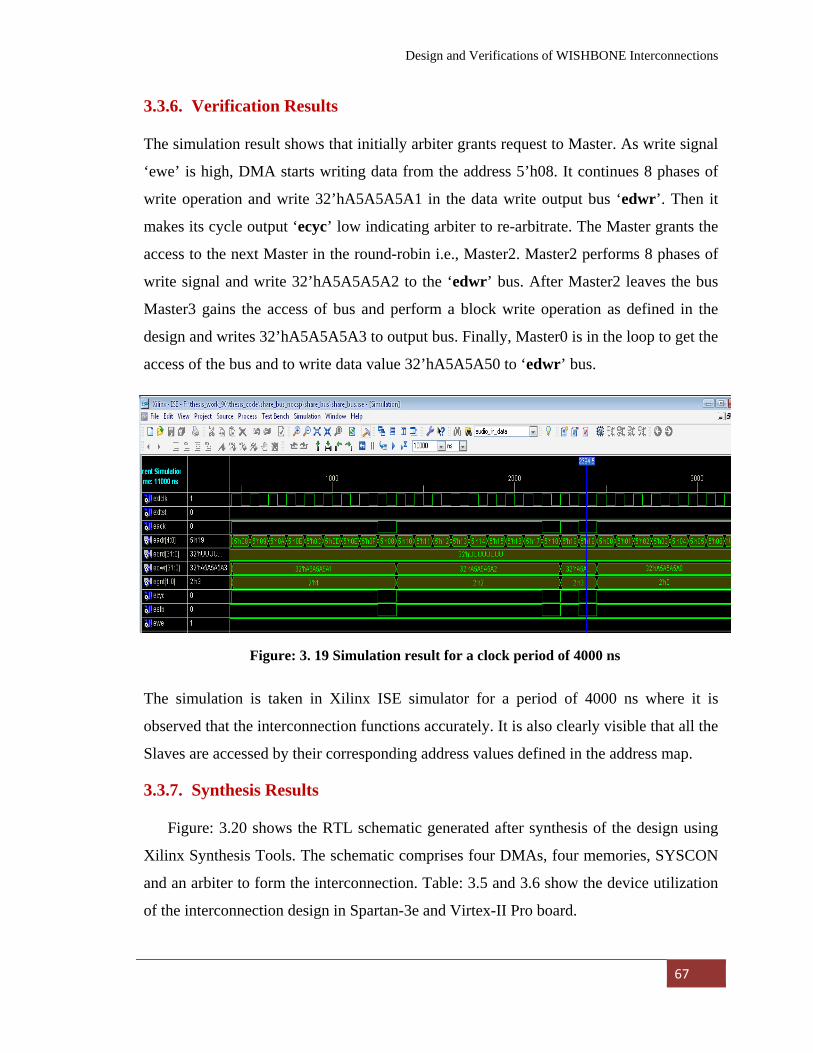
Design and Verifications of WISHBONE Interconnections
67
3.3.6. Verification Results
The simulation result shows that initially arbiter grants request to Master. As write signal
‘ewe’ is high, DMA starts writing data from the address 5’h08. It continues 8 phases of
write operation and write 32’hA5A5A5A1 in the data write output bus ‘edwr’. Then it
makes its cycle output ‘ecyc’ low indicating arbiter to re-arbitrate. The Master grants the
access to the next Master in the round-robin i.e., Master2. Master2 performs 8 phases of
write signal and write 32’hA5A5A5A2 to the ‘edwr’ bus. After Master2 leaves the bus
Master3 gains the access of bus and perform a block write operation as defined in the
design and writes 32’hA5A5A5A3 to output bus. Finally, Master0 is in the loop to get the
access of the bus and to write data value 32’hA5A5A50 to ‘edwr’ bus.
The simulation is taken in Xilinx ISE simulator for a period of 4000 ns where it is
observed that the interconnection functions accurately. It is also clearly visible that all the
Slaves are accessed by their corresponding address values defined in the address map.
3.3.7. Synthesis Results
Figure: 3.20 shows the RTL schematic generated after synthesis of the design using
Xilinx Synthesis Tools. The schematic comprises four DMAs, four memories, SYSCON
and an arbiter to form the interconnection. Table: 3.5 and 3.6 show the device utilization
of the interconnection design in Spartan-3e and Virtex-II Pro board.
Figure: 3. 19 Simulation result for a clock period of 4000 ns
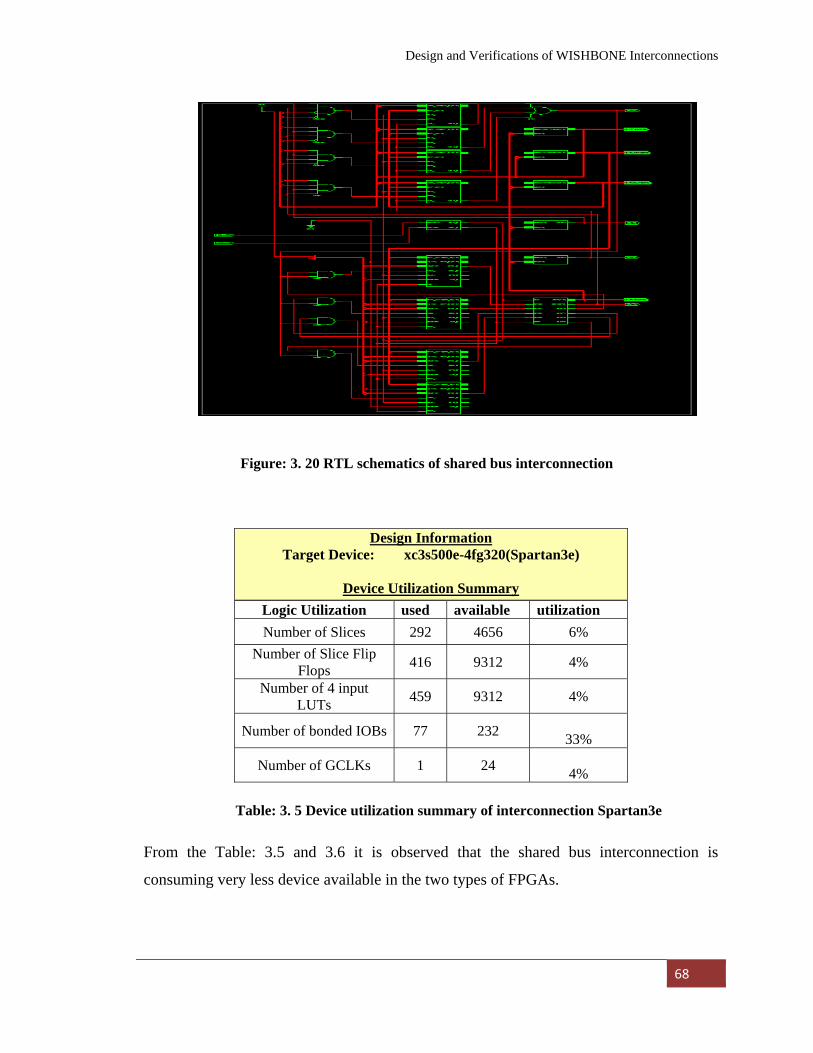
Design and Verifications of WISHBONE Interconnections
68
From the Table: 3.5 and 3.6 it is observed that the shared bus interconnection is
consuming very less device available in the two types of FPGAs.
Design Information Target Device: xc3s500e-4fg320(Spartan3e)
Device Utilization Summary
Logic Utilization used available utilization Number of Slices 292 4656 6%
Number of Slice Flip Flops 416 9312 4%
Number of 4 input LUTs 459 9312 4%
Number of bonded IOBs 77 232 33%
Number of GCLKs 1 24 4%
Table: 3. 5 Device utilization summary of interconnection Spartan3e
Figure: 3. 20 RTL schematics of shared bus interconnection
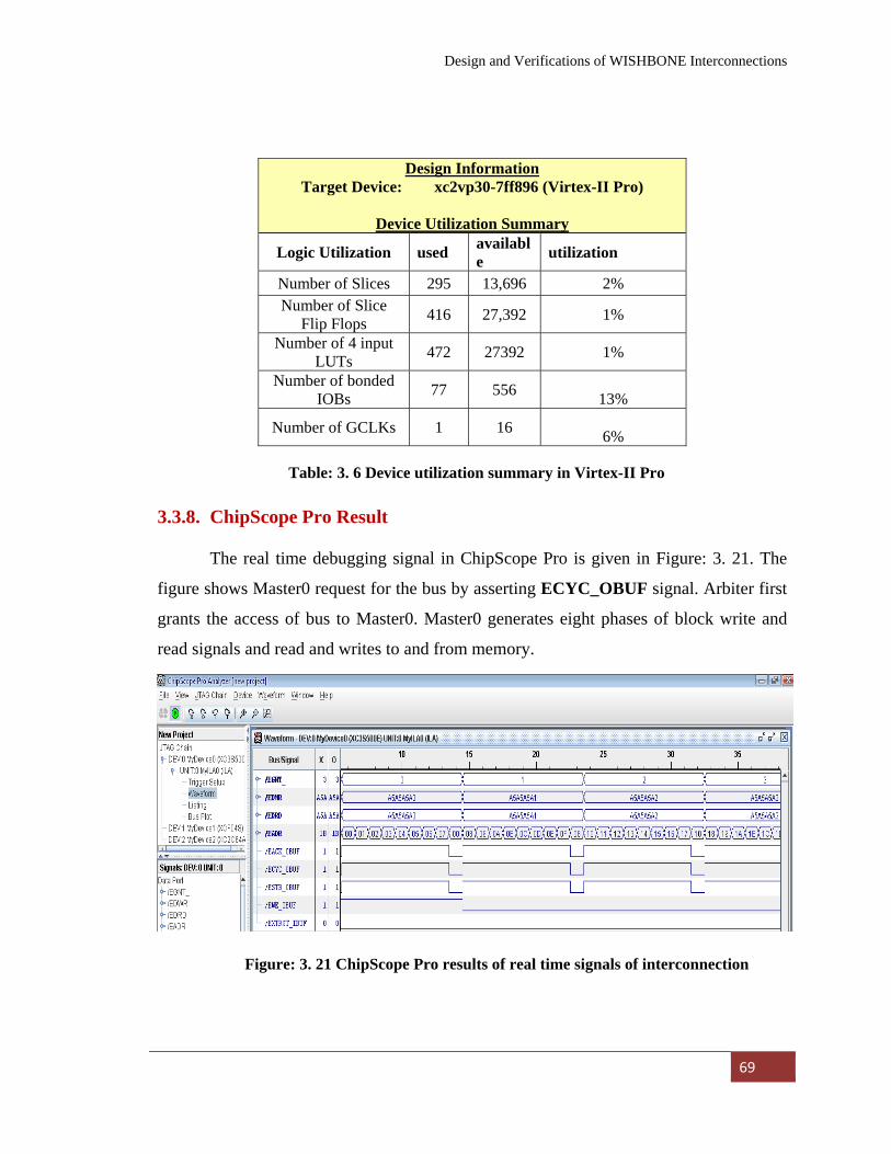
Design and Verifications of WISHBONE Interconnections
69
3.3.8. ChipScope Pro Result
The real time debugging signal in ChipScope Pro is given in Figure: 3. 21. The
figure shows Master0 request for the bus by asserting ECYC_OBUF signal. Arbiter first
grants the access of bus to Master0. Master0 generates eight phases of block write and
read signals and read and writes to and from memory.
Design Information Target Device: xc2vp30-7ff896 (Virtex-II Pro)
Device Utilization Summary
Logic Utilization used available utilization
Number of Slices 295 13,696 2% Number of Slice
Flip Flops 416 27,392 1%
Number of 4 input LUTs 472 27392 1%
Number of bonded IOBs 77 556
13%
Number of GCLKs 1 16 6%
Table: 3. 6 Device utilization summary in Virtex-II Pro
Figure: 3. 21 ChipScope Pro results of real time signals of interconnection
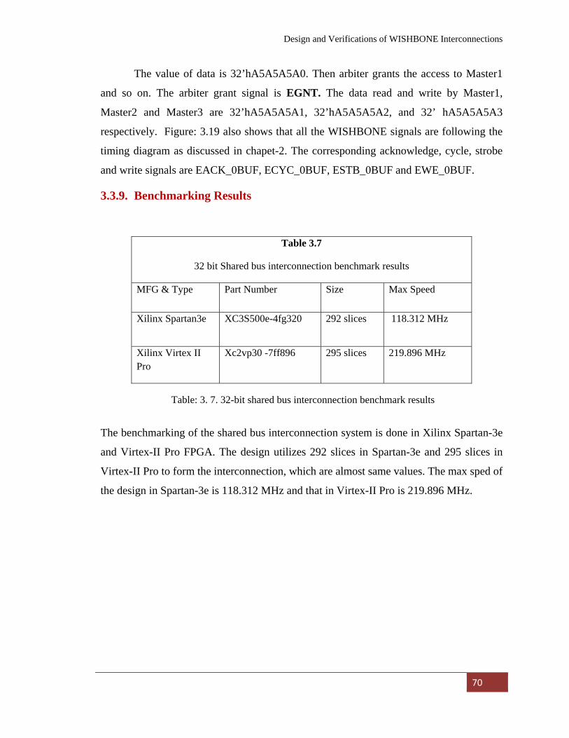
Design and Verifications of WISHBONE Interconnections
70
The value of data is 32’hA5A5A5A0. Then arbiter grants the access to Master1
and so on. The arbiter grant signal is EGNT. The data read and write by Master1,
Master2 and Master3 are 32’hA5A5A5A1, 32’hA5A5A5A2, and 32’ hA5A5A5A3
respectively. Figure: 3.19 also shows that all the WISHBONE signals are following the
timing diagram as discussed in chapet-2. The corresponding acknowledge, cycle, strobe
and write signals are EACK_0BUF, ECYC_0BUF, ESTB_0BUF and EWE_0BUF.
3.3.9. Benchmarking Results
The benchmarking of the shared bus interconnection system is done in Xilinx Spartan-3e
and Virtex-II Pro FPGA. The design utilizes 292 slices in Spartan-3e and 295 slices in
Virtex-II Pro to form the interconnection, which are almost same values. The max sped of
the design in Spartan-3e is 118.312 MHz and that in Virtex-II Pro is 219.896 MHz.
Table 3.7
32 bit Shared bus interconnection benchmark results
MFG & Type Part Number Size Max Speed
Xilinx Spartan3e XC3S500e-4fg320 292 slices 118.312 MHz
Xilinx Virtex II Pro
Xc2vp30 -7ff896 295 slices 219.896 MHz
Table: 3. 7. 32-bit shared bus interconnection benchmark results
Design and Verifications of WISHBONE Interconnections
71
3.4. Conclusions
Two types of interconnection topology have been created and its related design issues
are discussed. Initially a Slave core of 16-bit output of 8-bit granularity has taken and
the issues related to making it WISHBONE compatible has been discussed. A 32-bit
point-to-point and shared bus interconnection are designed and related issues are
discussed. The verification of the design is done using XILINX ISE simulator. Finally, by
using ChipScope Pro provided by Xilinx the proper functionality of the designed systems
are observed
The following conclusions are made from the above discussion:
• WISHBONE interface requires a very little logic overhead to implement the
entire interface. This gives rise to a highly portable system design that works with
standard, synchronous and combinatorial logic primitives available in most of the
FPGA and ASIC devices.
• The benchmarking results show that it also utilizes a very less logic to form the
interconnection. The minimum size requires for implementing point-to-point
interconnection is approximately 40 slices and for shared bus interconnection is
292 slices. Both the interconnection supports an operating frequency of more than
100 MHz. It is also observed that the maximum operating frequency of the design
depends on the target device technology. For high speed FPGA like Virtex-II Pro
the frequency is higher than the low speed FPGA Spartan3e. Hence, it supports
variable timing specification.
Low cost, portable and time to market SOC can be designed successfully using
WISHBONE bus interface.

72
Proposed SOC Design Methodology
Hardware Gateway of SOC
Architecture
Descriptions of IP Cores
Conclusions
Chapter 4
SOC Architecture and Design Methodology
SOC Architecture and Design Methodology
73
After complete verification and benchmarking of two Wishbone bus
interconnections, this chapter illustrates the methodology for a portable SOC design for
laboratory applications. For this purpose a suitable SOC architecture has been taken and
the IP cores are collected from the Open Core site. Finally, these cores are integrated to
form the SOC. The cores specifications, internal architecture, CPU bus cycles are
explained in this chapter.
4.1 Proposed SoC Design Methodology This section presents a description of design methodology adopted to implement a
SoC using Wishbone bus interface for laboratory applications. The complete design
methodology shown in Figure: 4.1 are consists of hardware design flow and software
design flow. These flows are described individually in the next section. The hardware
design flow is started with a collection of a set of IP cores and integrating them for a
chosen application, then arriving at the simulation step for verification of the entire SOC
design. Synthesis and implementation is done afterwards for ensuring the proper
hardware mapping & routing of SOC in FPGA. An application required to run in the
SOC hardware is being done by the software design flow. This can run in parallel with
the hardware design platform. Finally, the hardware model and software applications are
implemented in the real hardware. A complete verification and monitor checking is being
done for ensuring proper functionality of the system.
4.1.1 Hardware Design Flow
The SOC design steps begins with a collection of Open Core Project Aquarius
[23] aiming initially for an implementation of simple SOC architecture consisting of a
32-bit RISC processor (SuperH-2 compatible) and a set of peripherals for data
transmission with PC. The first step is to configure and adoption of the processor model
and the selection of any additional peripherals needed for the design. A set of IP cores of
32-bit RISC CPU Aquarius [ ], parallel input output (PIO), memory, system controller
and UART, were collected in a project directory and kept back for the future applications.
After the selection of IP cores and integrating same to desired SOC architecture, different
steps of the hardware design can be achieved in parallel, such as external hardware
interfacing, simulation and synthesis of the design. Aquarius developer provides a test
SOC Architecture and Design Methodology
74
bench with the project. A set of test bench have been developed in order to simulate the
hardware model. Icarus Verilog [19] tool is used to run this test bench to check the results
obtained are accurate to our application.
Figure: 4. 1 Design Methodology
A gate level net list is generated from a set of given RTL code for modeling the SOC
architecture into hardware. This is achieved by the synthesis step. Xilinx-Synthesis-Tool
[20] is used to compile the RTL behavior of SOC to generate a gate level net list for the
FPGA. Finally, implementation step is done where the gate level net list generated in the
previous step is used by Xilinx [20] place and route tools to do mapping, placing &
routing for target FPGA. A bit-stream file is generated to program the FPGA with the
SOC Architecture and Design Methodology
75
hardware model obtained in the complete flow. The additional hardware needed for the
application is developed and connected with the FPGA.
4.1.2 Software Design Flow Software design flow usually runs in parallel to the hardware design flow. This
section explains the design flow for software applications and the tools provided for
designer to choose for the work.
The simulator of Verilog-HDL codes and the compiler/assembler of the
application code development run on the UNIX environment. Cygwin [21] is selected as
the preferred environment for this purpose. To simulate verification program and to
develop the application program, the SuperH-2 [22] assembler and compiler are
necessary. GNU tool chain is preferred which can be used by the designer for software
development. The other steps involve compilation, debugging and implementation of the
software on the hardware. The project in Open Core provided with simple and useful
resources for logic verification and application code development. Application codes are
developed in C and compiled with GCC compiler. Debugging the application is an
important step in the software development flow, to validate the results obtained with the
program in the SOC. This is done by GNU GDB [24] debugger. Finally, by using
monitor program the code is downloaded to SOC model dumped in the FPGA.
4.2 Hardware Gateway of SoC Architecture
Figure: 4. 2 Hardware gateway of SOC architecture
SOC Architecture and Design Methodology
76
The SOC architecture for laboratory application is shown in Figure: 4.2. This
architecture utilizes processor and peripherals from the Aquarius [23] project designed by
Thorn Aitch published in Open Core [4] under GPL license. The architecture consists of
a 32-bit SuperH-2 [22] compatible CPU MASTER, a memory unit (RAM and ROM
unit), a universal asynchronous receiver transmitter, a system controller and a parallel
input output. The cores are connected to each other through WISHBONE interface with a
point-to-point interconnection scheme. The next section describes about the detail
specifications and structures of IP cores used for building this SOC architecture.
4.3 Descriptions of IP Cores
4.3.1 CPU
I. Specification
• 32-bit 5-stage pipelined CPU • Instruction set is compatible with SuperH-2 [22 ]. (Renesas /Toshiba make)
• Instruction set supporting Power-on-reset, IRQ, NMI, address and DMA error.
• Bus interface is compatible with Wishbone.
• Sixteen 32-bit general purpose registers (R0-R16), SR, GBR, VBR, PR, PC.
• 32-bit x 16-bit multiplier and accumulator for DSP functionality.
• Low power sleep mode.
II. Structure of CPU
Figure: 4.3 shows the block diagram of the top modules of Aquarius CPU having
Wishbone compliant bus signal. The CPU is a RISC processor based on superH-2 [22]
Instruction set architecture. This synthesizable core written in Verilog and can be
implemented in FPGA. This is published under GPL license in Open Core site [4]. The
SuperH-2 is a 5-stage pipelined architecture with sixteen 32-bit general purpose registers.
It can handle interrupt requests like non-maskable interrupt (NMI) and interrupt request
(IRQ). In a lower hierarchy it comprises a memory access controller, a data path unit, a
multiply unit and a decoder unit [23].
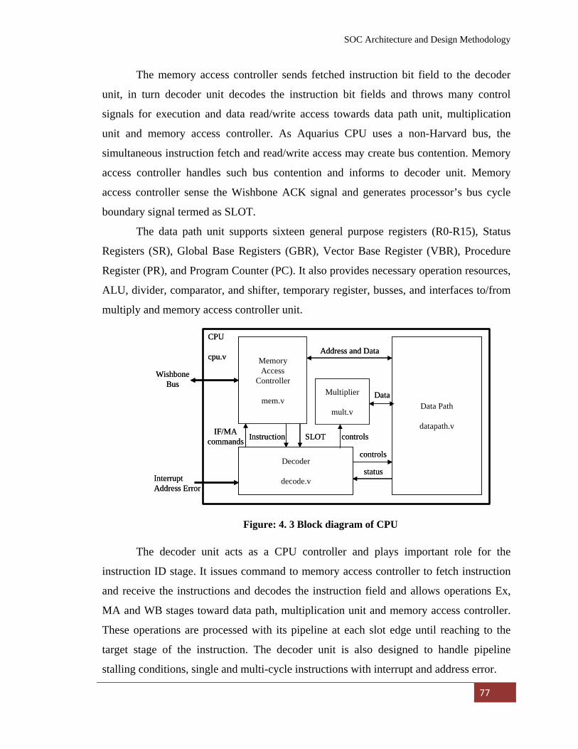
SOC Architecture and Design Methodology
77
MemoryAccess
Controller
mem.v
Decoder
decode.v
Data Path
datapath.v
WishboneBus
InterruptAddress Error
IF/MAcommands SLOT
controls
status
Multiplier
mult.v
Instruction controls
Data
Address and Data
CPU
cpu.v MemoryAccess
Controller
mem.v
Decoder
decode.v
Data Path
datapath.v
WishboneBus
InterruptAddress Error
IF/MAcommands SLOT
controls
status
Multiplier
mult.v
Instruction controls
Data
Address and Data
CPU
cpu.v
The memory access controller sends fetched instruction bit field to the decoder
unit, in turn decoder unit decodes the instruction bit fields and throws many control
signals for execution and data read/write access towards data path unit, multiplication
unit and memory access controller. As Aquarius CPU uses a non-Harvard bus, the
simultaneous instruction fetch and read/write access may create bus contention. Memory
access controller handles such bus contention and informs to decoder unit. Memory
access controller sense the Wishbone ACK signal and generates processor’s bus cycle
boundary signal termed as SLOT.
The data path unit supports sixteen general purpose registers (R0-R15), Status
Registers (SR), Global Base Registers (GBR), Vector Base Register (VBR), Procedure
Register (PR), and Program Counter (PC). It also provides necessary operation resources,
ALU, divider, comparator, and shifter, temporary register, busses, and interfaces to/from
multiply and memory access controller unit.
The decoder unit acts as a CPU controller and plays important role for the
instruction ID stage. It issues command to memory access controller to fetch instruction
and receive the instructions and decodes the instruction field and allows operations Ex,
MA and WB stages toward data path, multiplication unit and memory access controller.
These operations are processed with its pipeline at each slot edge until reaching to the
target stage of the instruction. The decoder unit is also designed to handle pipeline
stalling conditions, single and multi-cycle instructions with interrupt and address error.
Figure: 4. 3 Block diagram of CPU
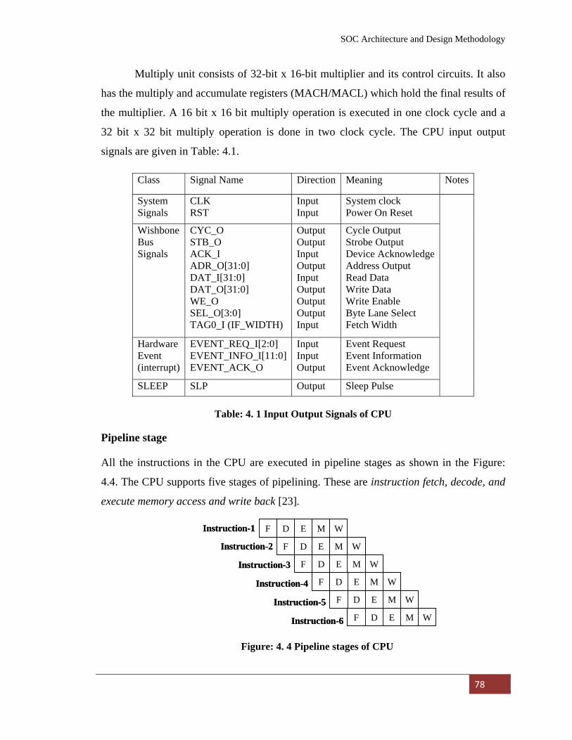
SOC Architecture and Design Methodology
78
F D E M W
F D E M W
F D E M W
F D E M W
F D E M W
F D E M W
Instruction-1
Instruction-2
Instruction-3
Instruction-4
Instruction-5
Instruction-6
F D E M W
F D E M W
F D E M W
F D E M W
F D E M W
F D E M W
Instruction-1
Instruction-2
Instruction-3
Instruction-4
Instruction-5
Instruction-6
Multiply unit consists of 32-bit x 16-bit multiplier and its control circuits. It also
has the multiply and accumulate registers (MACH/MACL) which hold the final results of
the multiplier. A 16 bit x 16 bit multiply operation is executed in one clock cycle and a
32 bit x 32 bit multiply operation is done in two clock cycle. The CPU input output
signals are given in Table: 4.1.
Class Signal Name Direction Meaning Notes
System Signals
CLK RST
Input Input
System clock Power On Reset
Wishbone Bus Signals
CYC_O STB_O ACK_I ADR_O[31:0] DAT_I[31:0] DAT_O[31:0] WE_O SEL_O[3:0] TAG0_I (IF_WIDTH)
Output Output Input Output Input Output Output Output Input
Cycle Output Strobe Output Device Acknowledge Address Output Read Data Write Data Write Enable Byte Lane Select Fetch Width
Hardware Event (interrupt)
EVENT_REQ_I[2:0] EVENT_INFO_I[11:0] EVENT_ACK_O
Input Input Output
Event Request Event Information Event Acknowledge
SLEEP SLP Output Sleep Pulse
Table: 4. 1 Input Output Signals of CPU
Pipeline stage
All the instructions in the CPU are executed in pipeline stages as shown in the Figure:
4.4. The CPU supports five stages of pipelining. These are instruction fetch, decode, and
execute memory access and write back [23].
Figure: 4. 4 Pipeline stages of CPU
SOC Architecture and Design Methodology
79
1) IF : Instruction fetch (F)
In this stage CPU fetches instruction code from memory. Depending upon the bus width,
the IF stage fetch the number of instructions. The instruction length is 16 bit. So in a 32-
bit bus width, IF stage fetches 2 instructions.
2) ID: Decode(D)
The ID stage controls the whole CPU operation by decoding fetched instructions.
The ID stage issues many control signals to perform Ex, MA and WB operations towards
data path, and memory access controller units. If multiplication operation is required, it
activates the multiplication unit. The signals shift to each stage in pipeline and activates
the corresponding each stage. ID also issues IF stage for next instruction and IF forward
new instruction to the corresponding ID stages. It also control the operation during
hardware event exceptions.
3) EX: Execute
After getting control from the ID stage, the EX stage performs register-register
operation or calculate address for next MA stage. This is done by data path unit.
Executions of multiplication commands are handled by multiplier unit.
4) MA: Memory Access
If memory access gets control signal by ID stage, then the MA reads/writes data
to/from memory. Due to non-Harvard bus used in the CPU, the MA has the highest
priority than IF stage to avoid bus contention.
5) WB: Write Back
If WB is invoked by ID stage, then WB writes back the memory read data to the
registers (R0-R16).
Pipeline stages of instructions
Figure: 4.5 shows the pipelining stages of some typical instructions. It shows all
instructions do not always need 5 stages for execution. The register-register operation
requires 3 stages; IF, ID and EX. All the operation register read, write, ALU operation,
executed in EX stage. The instruction for storing into memory requires 4 stages; IF, ID,
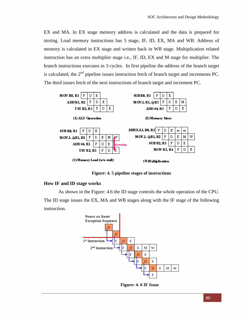
SOC Architecture and Design Methodology
80
D
D
F
F
D
D
E
E M W
F D E
F D E
F D E M W
F
Power on ResetException Sequence
1st Instruction
2nd Instruction
D
D
F
F
D
D
E
E M W
F D E
F D E
F D E M W
F
Power on ResetException Sequence
1st Instruction
2nd Instruction
EX and MA. In EX stage memory address is calculated and the data is prepared for
storing. Load memory instructions has 5 stage, IF, ID, EX, MA and WB. Address of
memory is calculated in EX stage and written back in WB stage. Multiplication related
instruction has an extra multiplier stage i.e., IF, ID, EX and M stage for multiplier. The
branch instructions executes in 3 cycles. In first pipeline the address of the branch target
is calculated, the 2nd pipeline issues instruction fetch of branch target and increments PC.
The third issues fetch of the next instructions of branch target and increment PC.
Figure: 4. 5 pipeline stages of instructions
How IF and ID stage works
As shown in the Figure: 4.6 the ID stage controls the whole operation of the CPU.
The ID stage issues the EX, MA and WB stages along with the IF stage of the following
instruction.
Figure: 4. 6 IF Issue
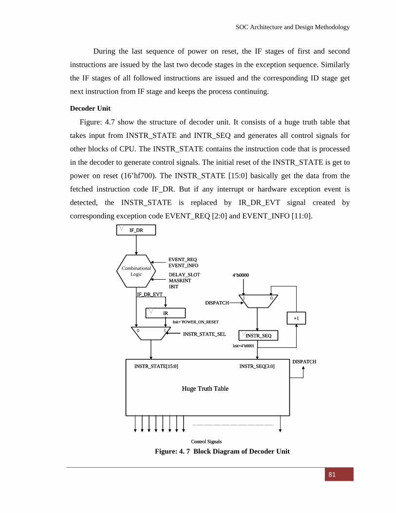
SOC Architecture and Design Methodology
81
IF_DR
EVENT_REQEVENT_INFO
IF_DR_EVT
IR
0 1
INSTR_STATE[15:0]
INSTR_STATE_SEL
CombinationalLogic DELAY_SLOT
MASKINTIBIT
INSTR_SEQ[3:0]
INSTR_SEQ
+1
4’b0000
Huge Truth Table
Control Signals
Init=4’b0001
DISPATCH1 0
DISPATCH
Init=`POWER_ON_RESET
IF_DR
EVENT_REQEVENT_INFO
IF_DR_EVT
IR
0 1
INSTR_STATE[15:0]
INSTR_STATE_SEL
CombinationalLogic DELAY_SLOT
MASKINTIBIT
INSTR_SEQ[3:0]
INSTR_SEQ
+1
4’b0000
Huge Truth Table
Control Signals
Init=4’b0001
DISPATCH1 0
DISPATCH
Init=`POWER_ON_RESET
During the last sequence of power on reset, the IF stages of first and second
instructions are issued by the last two decode stages in the exception sequence. Similarly
the IF stages of all followed instructions are issued and the corresponding ID stage get
next instruction from IF stage and keeps the process continuing.
Decoder Unit
Figure: 4.7 show the structure of decoder unit. It consists of a huge truth table that
takes input from INSTR_STATE and INTR_SEQ and generates all control signals for
other blocks of CPU. The INSTR_STATE contains the instruction code that is processed
in the decoder to generate control signals. The initial reset of the INSTR_STATE is get to
power on reset (16’hf700). The INSTR_STATE [15:0] basically get the data from the
fetched instruction code IF_DR. But if any interrupt or hardware exception event is
detected, the INSTR_STATE is replaced by IR_DR_EVT signal created by
corresponding exception code EVENT_REQ [2:0] and EVENT_INFO [11:0].
Figure: 4. 7 Block Diagram of Decoder Unit
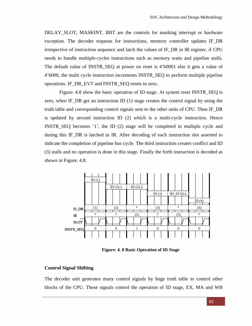
SOC Architecture and Design Methodology
82
ID (1)
ID (2)-1 ID (2)-2
ID (3) ID_STALL
(1)IF_DR
IR *
ID (4)
(2)
(2)*
* (3) *
(3)*
(4)
*
SLOT
0 0 1 0 0 0INSTR_SEQ
ID (1)
ID (2)-1 ID (2)-2
ID (3) ID_STALL
(1)IF_DR
IR *
ID (4)
(2)
(2)*
* (3) *
(3)*
(4)
*
SLOT
0 0 1 0 0 0INSTR_SEQ
DELAY_SLOT, MASKINT, IBIT are the controls for masking interrupt or hardware
exception. The decoder requests for instructions, memory controller updates IF_DR
irrespective of instruction sequence and latch the values of IF_DR in IR register, if CPU
needs to handle multiple-cycles instructions such as memory waits and pipeline stalls.
The default value of INSTR_SEQ at power on reset is 4’b0001 else it gets a value of
4’b000, the multi cycle instruction increments INSTR_SEQ to perform multiple pipeline
operations. IF_DR_EVT and INSTR_SEQ resets to zero.
Figure: 4.8 show the basic operation of ID stage. At system reset INSTR_SEQ is
zero, when IF_DR get an instruction ID (1) stage creates the control signal by using the
truth table and corresponding control signals sent to the other units of CPU. Then IF_DR
is updated by second instruction ID (2) which is a multi-cycle instruction. Hence
INSTR_SEQ becomes ‘1’, the ID (2) stage will be completed in multiple cycle and
during this IF_DR is latched in IR. After decoding of each instruction slot asserted to
indicate the completion of pipeline bus cycle. The third instruction creates conflict and ID
(3) stalls and no operation is done in this stage. Finally the forth instruction is decoded as
shown in Figure: 4.8.
Control Signal Shifting
The decoder unit generates many control signals by huge truth table to control other
blocks of the CPU. These signals control the operation of ID stage, EX, MA and WB
Figure: 4. 8 Basic Operation of ID Stage
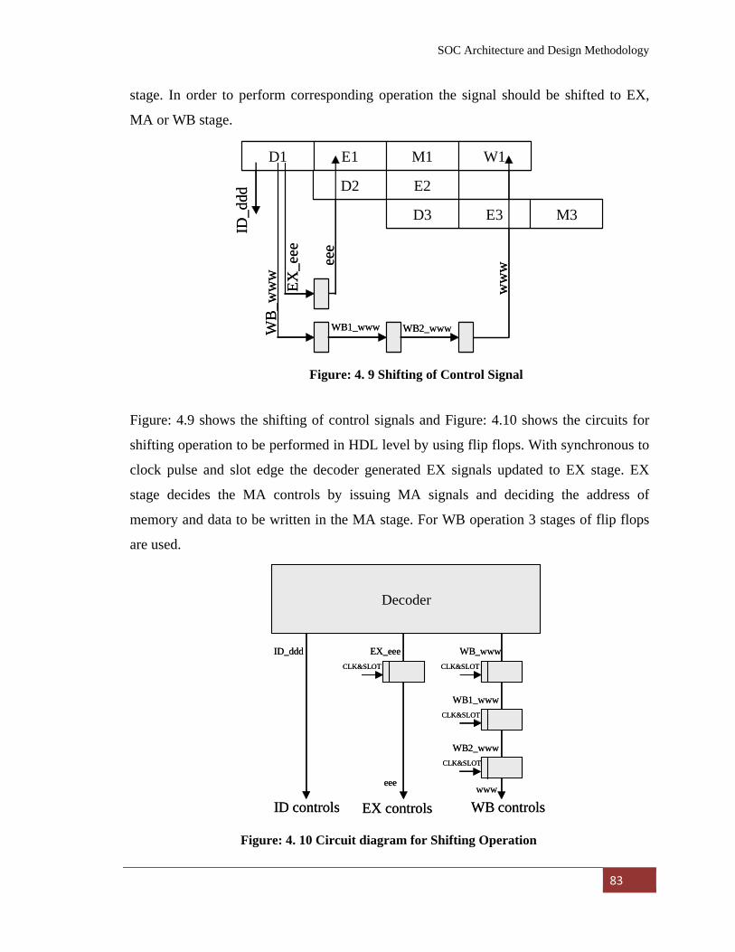
SOC Architecture and Design Methodology
83
D1 E1 M1 W1
D2 E2
E3 M3
EX_e
ee eee
D3
WB_
ww
w
WB1_www WB2_www
ww
w
ID_d
dd
D1 E1 M1 W1
D2 E2
E3 M3
EX_e
ee eee
D3
WB_
ww
w
WB1_www WB2_www
ww
w
ID_d
dd
Decoder
EX controls WB controls
CLK&SLOT CLK&SLOT
CLK&SLOT
CLK&SLOT
EX_eee
eee
WB_www
WB1_www
WB2_www
www
ID controls
ID_ddd
Decoder
EX controls WB controls
CLK&SLOT CLK&SLOT
CLK&SLOT
CLK&SLOT
EX_eee
eee
WB_www
WB1_www
WB2_www
www
ID controls
ID_ddd
stage. In order to perform corresponding operation the signal should be shifted to EX,
MA or WB stage.
Figure: 4.9 shows the shifting of control signals and Figure: 4.10 shows the circuits for
shifting operation to be performed in HDL level by using flip flops. With synchronous to
clock pulse and slot edge the decoder generated EX signals updated to EX stage. EX
stage decides the MA controls by issuing MA signals and deciding the address of
memory and data to be written in the MA stage. For WB operation 3 stages of flip flops
are used.
Figure: 4. 9 Shifting of Control Signal
Figure: 4. 10 Circuit diagram for Shifting Operation
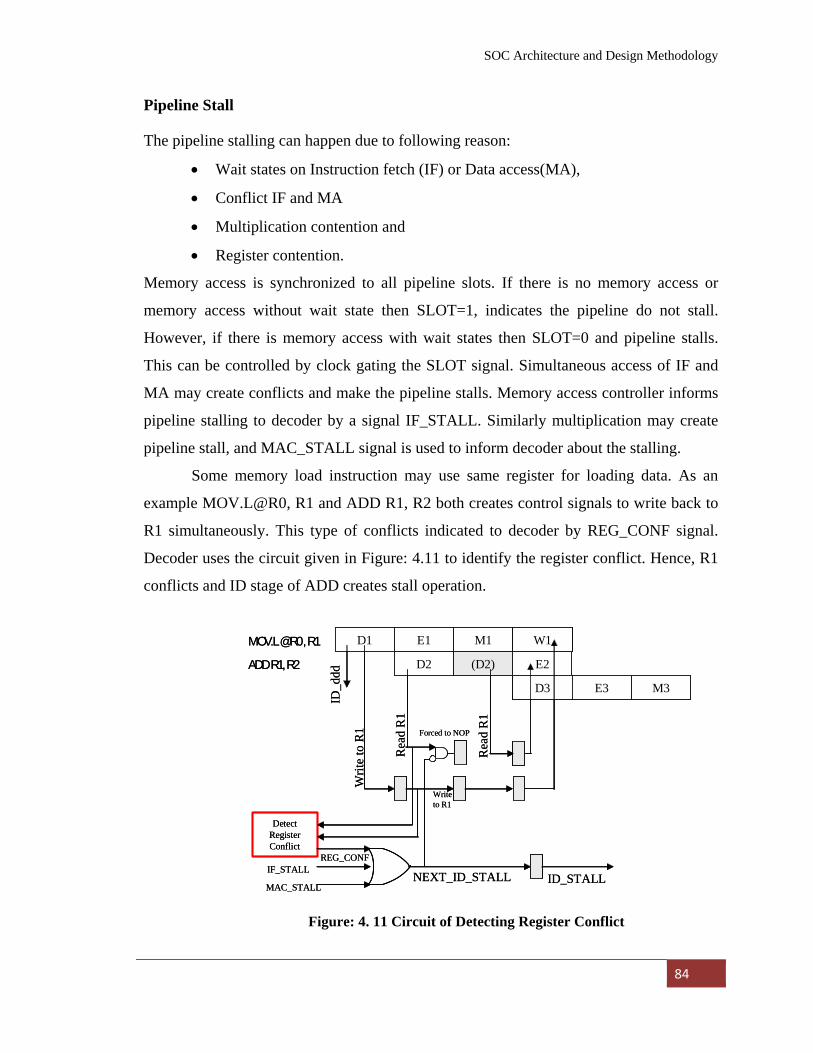
SOC Architecture and Design Methodology
84
D1 E1 M1 W1
D2 E2
E3 M3
Rea
d R
1
D3
Writ
e to
R1
Writeto R1
ID_d
dd
MOV.L @R0, R1
ADD R1, R2
DetectRegisterConflict
(D2)
Rea
d R
1
Forced to NOP
NEXT_ID_STALL ID_STALL
REG_CONFIF_STALL
MAC_STALL
D1 E1 M1 W1
D2 E2
E3 M3
Rea
d R
1
D3
Writ
e to
R1
Writeto R1
ID_d
dd
MOV.L @R0, R1
ADD R1, R2
DetectRegisterConflict
(D2)
Rea
d R
1
Forced to NOP
NEXT_ID_STALL ID_STALL
REG_CONFIF_STALL
MAC_STALL
Pipeline Stall
The pipeline stalling can happen due to following reason:
• Wait states on Instruction fetch (IF) or Data access(MA),
• Conflict IF and MA
• Multiplication contention and
• Register contention.
Memory access is synchronized to all pipeline slots. If there is no memory access or
memory access without wait state then SLOT=1, indicates the pipeline do not stall.
However, if there is memory access with wait states then SLOT=0 and pipeline stalls.
This can be controlled by clock gating the SLOT signal. Simultaneous access of IF and
MA may create conflicts and make the pipeline stalls. Memory access controller informs
pipeline stalling to decoder by a signal IF_STALL. Similarly multiplication may create
pipeline stall, and MAC_STALL signal is used to inform decoder about the stalling.
Some memory load instruction may use same register for loading data. As an
example MOV.L@R0, R1 and ADD R1, R2 both creates control signals to write back to
R1 simultaneously. This type of conflicts indicated to decoder by REG_CONF signal.
Decoder uses the circuit given in Figure: 4.11 to identify the register conflict. Hence, R1
conflicts and ID stage of ADD creates stall operation.
Figure: 4. 11 Circuit of Detecting Register Conflict
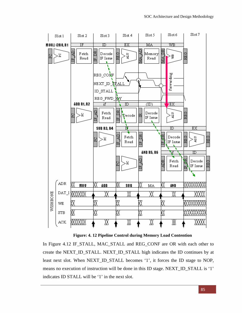
SOC Architecture and Design Methodology
85
In Figure 4.12 IF_STALL, MAC_STALL and REG_CONF are OR with each other to
create the NEXT_ID_STALL. NEXT_ID_STALL high indicates the ID continues by at
least next slot. When NEXT_ID_STALL becomes ‘1’, it forces the ID stage to NOP,
means no execution of instruction will be done in this ID stage. NEXT_ID_STALL is ‘1’
indicates ID STALL will be ‘1’ in the next slot.
Figure: 4. 12 Pipeline Control during Memory Load Contention
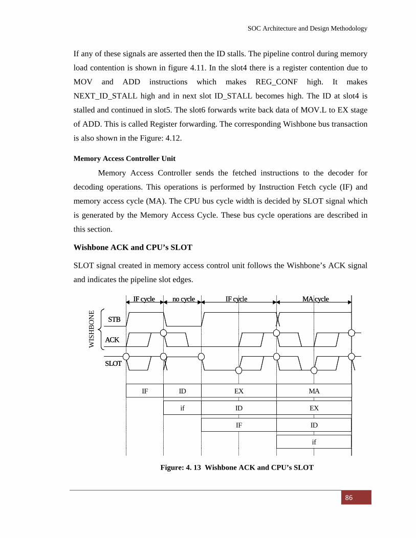
SOC Architecture and Design Methodology
86
STB
IF cycle
ACK
IF cycle MA cycle
SLOT
WIS
HBO
NE
IF ID EX
if ID
IF
MA
EX
ID
no cycle
if
STB
IF cycle
ACK
IF cycle MA cycle
SLOT
WIS
HBO
NE
IF ID EX
if ID
IF
MA
EX
ID
no cycle
if
If any of these signals are asserted then the ID stalls. The pipeline control during memory
load contention is shown in figure 4.11. In the slot4 there is a register contention due to
MOV and ADD instructions which makes REG_CONF high. It makes
NEXT_ID_STALL high and in next slot ID_STALL becomes high. The ID at slot4 is
stalled and continued in slot5. The slot6 forwards write back data of MOV.L to EX stage
of ADD. This is called Register forwarding. The corresponding Wishbone bus transaction
is also shown in the Figure: 4.12.
Memory Access Controller Unit
Memory Access Controller sends the fetched instructions to the decoder for
decoding operations. This operations is performed by Instruction Fetch cycle (IF) and
memory access cycle (MA). The CPU bus cycle width is decided by SLOT signal which
is generated by the Memory Access Cycle. These bus cycle operations are described in
this section.
Wishbone ACK and CPU’s SLOT
SLOT signal created in memory access control unit follows the Wishbone’s ACK signal
and indicates the pipeline slot edges.
Figure: 4. 13 Wishbone ACK and CPU’s SLOT
SOC Architecture and Design Methodology
87
To control the pipeline stall from MA cycle all the flip flop in the CPU are gated with
SLOT signal. Figure 4.13 shows the wave form of the SLOT is similar to the ACK,
except that the SLOT is asserted if no memory access cycle is encountered. During
memory accessed operation the SLOT signal wave form follows to ACK signal.
Instruction Fetch Cycle
The decoder unit requests instruction fetch to the memory access control unit by
issuing IF_ISSUE signal. The instruction fetch starts in the next slot after assertion of
IF_ISSUE. During this time the IF_AD [31:0] and IF_JP should be valid state. The
address value of the fetched instruction is given by IF_AD[31:0].
Figure 4.14 shows the waveform of an instruction fetch cycle. Initially when
IF_ISSUE is asserted, the IF_AD contains the address of second instruction IF(2). At the
next slot the instruction fetch starts and the value is latched to IF_DR. WISHBONE
Signal initiates a single read cycle reflects the data transfer by asserting the STB signal.
ADR contains the address of IF(2). DAT_I read the IF(2) value and latch this value in
IF_DR of decoder for decoding. The ACK shows the termination of this cycle.
If instruction fetch is created by jump or branch instruction, the fetch should access the
memory even if the internal fetch buffer is valid. Hence jumping operation should inform
such state to memory access control unit by asserting IF_JP and IF_ISSUE at a time.
IF_DR [15:0] is valid at the next slot of corresponding IF cycle. The second assertion in
IF_ISSUE in the Figure: 4.14 reflect the same situation. Due to branch instruction IF_DR
gets IF(3) after second IF cycle is completed.
Memory Access Cycle
Similar to instruction fetch, MA starts at next slot of MA_ISSUE becomes high. Some
attribute information such as access size MA_SZ [1:0], access direction MA_RW,
address MA_AD [31:0] and if write access, write data MA_WD [31:0] should be valid
when MA_ISSUE is high.
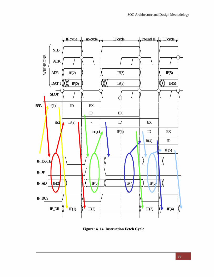
SOC Architecture and Design Methodology
88
STB
IF cycle
ACK
IF cycle IF cycle
SLOT
WIS
HBO
NE
if(1) ID EX
IF(2) ID
IF(3)
EX
ID
no cycle
if(4) ID
EX
IF_ISSUE
Internal IF
IF(2) IF(3)ADR
IF(5)
IF(5)
IF(2) IF(3)DAT_I IF(5)
EX
BRA
slot -
target
ID
IF_JP
IF_AD IF(2) IF(3) IF(4) IF(5)
IF_BUS
IF(2) IF(3) IF(4)IF_DR IF(1)
STB
IF cycle
ACK
IF cycle IF cycle
SLOT
WIS
HBO
NE
if(1) ID EX
IF(2) ID
IF(3)
EX
ID
no cycle
if(4) ID
EX
IF_ISSUE
Internal IF
IF(2) IF(3)ADR
IF(5)
IF(5)
IF(2) IF(3)DAT_I IF(5)
EX
BRA
slot -
target
ID
IF_JP
IF_AD IF(2) IF(3) IF(4) IF(5)
IF_BUS
IF(2) IF(3) IF(4)IF_DR IF(1)
Figure: 4. 14 Instruction Fetch Cycle
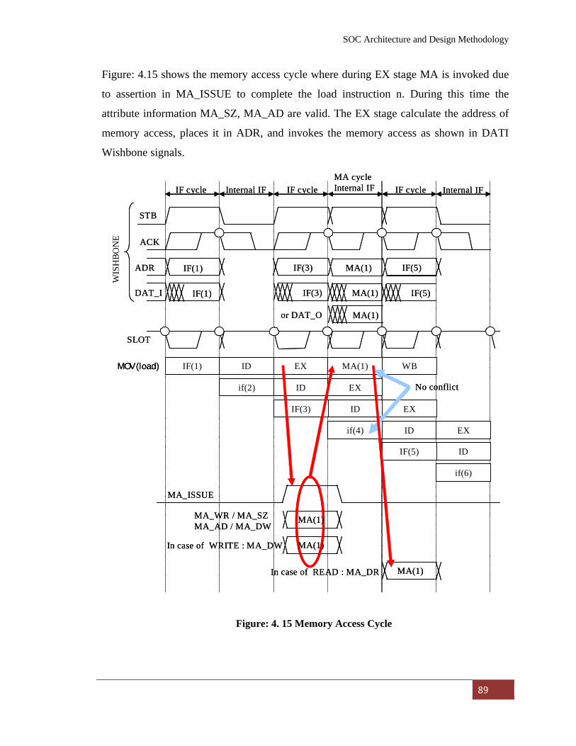
SOC Architecture and Design Methodology
89
STB
IF cycle
ACK
IF cycle IF cycle
SLOT
WIS
HBO
NE
IF(1) ID EX
Internal IF
MA_ISSUE
MA cycleInternal IF
IF(1) IF(3)ADR IF(5)
IF(1) IF(3)DAT_I
MOV (load)
MA_WR / MA_SZMA_AD / MA_DW
MA(1) WB
if(2) ID EX
IF(3) ID EX
if(4) ID EX
IF(5) ID
if(6)
Internal IF
MA(1)
MA(1) IF(5)
MA(1)or DAT_O
No conflict
MA(1)
MA(1)
MA(1)
In case of WRITE : MA_DW
In case of READ : MA_DR
Figure: 4.15 shows the memory access cycle where during EX stage MA is invoked due
to assertion in MA_ISSUE to complete the load instruction n. During this time the
attribute information MA_SZ, MA_AD are valid. The EX stage calculate the address of
memory access, places it in ADR, and invokes the memory access as shown in DATI
Wishbone signals.
Figure: 4. 15 Memory Access Cycle
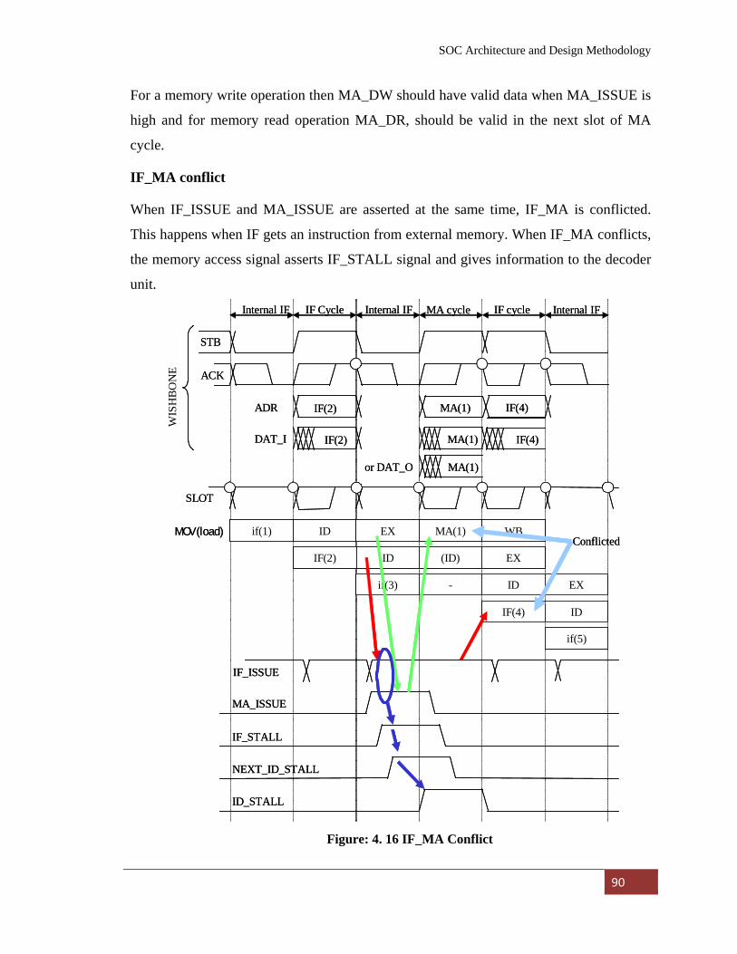
SOC Architecture and Design Methodology
90
STB
Internal IF
ACK
Internal IF IF cycle
SLOT
WIS
HBO
NE
if(1) ID EX
IF Cycle
IF_ISSUE
MA cycle
IF(2)ADR IF(4)
IF(2)DAT_I
MOV (load) MA(1) WB
IF(2) ID EX
if(3) ID EX
IF(4) ID
if(5)
Internal IF
MA(1)
MA(1) IF(4)
MA(1)or DAT_O
(ID)
-
Conflicted
MA_ISSUE
IF_STALL
NEXT_ID_STALL
ID_STALL
STB
Internal IF
ACK
Internal IF IF cycle
SLOT
WIS
HBO
NE
if(1) ID EX
IF Cycle
IF_ISSUE
MA cycle
IF(2)ADR IF(4)
IF(2)DAT_I
MOV (load) MA(1) WB
IF(2) ID EX
if(3) ID EX
IF(4) ID
if(5)
Internal IF
MA(1)
MA(1) IF(4)
MA(1)or DAT_O
(ID)
-
Conflicted
MA_ISSUE
IF_STALL
NEXT_ID_STALL
ID_STALL
For a memory write operation then MA_DW should have valid data when MA_ISSUE is
high and for memory read operation MA_DR, should be valid in the next slot of MA
cycle.
IF_MA conflict
When IF_ISSUE and MA_ISSUE are asserted at the same time, IF_MA is conflicted.
This happens when IF gets an instruction from external memory. When IF_MA conflicts,
the memory access signal asserts IF_STALL signal and gives information to the decoder
unit.
Figure: 4. 16 IF_MA Conflict
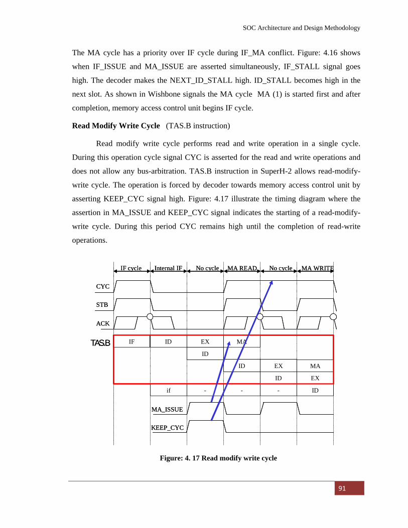
SOC Architecture and Design Methodology
91
IF ID EX
ID
ID EX
MA
MA
ID EX
TAS.B
if ID- - -
CYC
IF cycle No cycle No cycleInternal IF MA READ MA WRITE
ACK
STB
MA_ISSUE
KEEP_CYC
IF ID EX
ID
ID EX
MA
MA
ID EX
TAS.B
if ID- - -
CYC
IF cycle No cycle No cycleInternal IF MA READ MA WRITE
ACK
STB
MA_ISSUE
KEEP_CYC
The MA cycle has a priority over IF cycle during IF_MA conflict. Figure: 4.16 shows
when IF_ISSUE and MA_ISSUE are asserted simultaneously, IF_STALL signal goes
high. The decoder makes the NEXT_ID_STALL high. ID_STALL becomes high in the
next slot. As shown in Wishbone signals the MA cycle MA (1) is started first and after
completion, memory access control unit begins IF cycle.
Read Modify Write Cycle (TAS.B instruction)
Read modify write cycle performs read and write operation in a single cycle.
During this operation cycle signal CYC is asserted for the read and write operations and
does not allow any bus-arbitration. TAS.B instruction in SuperH-2 allows read-modify-
write cycle. The operation is forced by decoder towards memory access control unit by
asserting KEEP_CYC signal high. Figure: 4.17 illustrate the timing diagram where the
assertion in MA_ISSUE and KEEP_CYC signal indicates the starting of a read-modify-
write cycle. During this period CYC remains high until the completion of read-write
operations.
Figure: 4. 17 Read modify write cycle
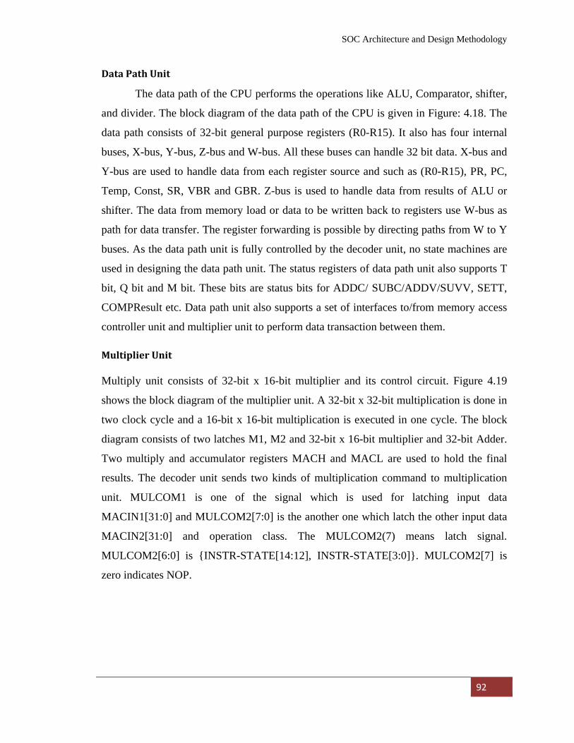
SOC Architecture and Design Methodology
92
Data Path Unit
The data path of the CPU performs the operations like ALU, Comparator, shifter,
and divider. The block diagram of the data path of the CPU is given in Figure: 4.18. The
data path consists of 32-bit general purpose registers (R0-R15). It also has four internal
buses, X-bus, Y-bus, Z-bus and W-bus. All these buses can handle 32 bit data. X-bus and
Y-bus are used to handle data from each register source and such as (R0-R15), PR, PC,
Temp, Const, SR, VBR and GBR. Z-bus is used to handle data from results of ALU or
shifter. The data from memory load or data to be written back to registers use W-bus as
path for data transfer. The register forwarding is possible by directing paths from W to Y
buses. As the data path unit is fully controlled by the decoder unit, no state machines are
used in designing the data path unit. The status registers of data path unit also supports T
bit, Q bit and M bit. These bits are status bits for ADDC/ SUBC/ADDV/SUVV, SETT,
COMPResult etc. Data path unit also supports a set of interfaces to/from memory access
controller unit and multiplier unit to perform data transaction between them.
Multiplier Unit
Multiply unit consists of 32-bit x 16-bit multiplier and its control circuit. Figure 4.19
shows the block diagram of the multiplier unit. A 32-bit x 32-bit multiplication is done in
two clock cycle and a 16-bit x 16-bit multiplication is executed in one cycle. The block
diagram consists of two latches M1, M2 and 32-bit x 16-bit multiplier and 32-bit Adder.
Two multiply and accumulator registers MACH and MACL are used to hold the final
results. The decoder unit sends two kinds of multiplication command to multiplication
unit. MULCOM1 is one of the signal which is used for latching input data
MACIN1[31:0] and MULCOM2[7:0] is the another one which latch the other input data
MACIN2[31:0] and operation class. The MULCOM2(7) means latch signal.
MULCOM2[6:0] is {INSTR-STATE[14:12], INSTR-STATE[3:0]}. MULCOM2[7] is
zero indicates NOP.
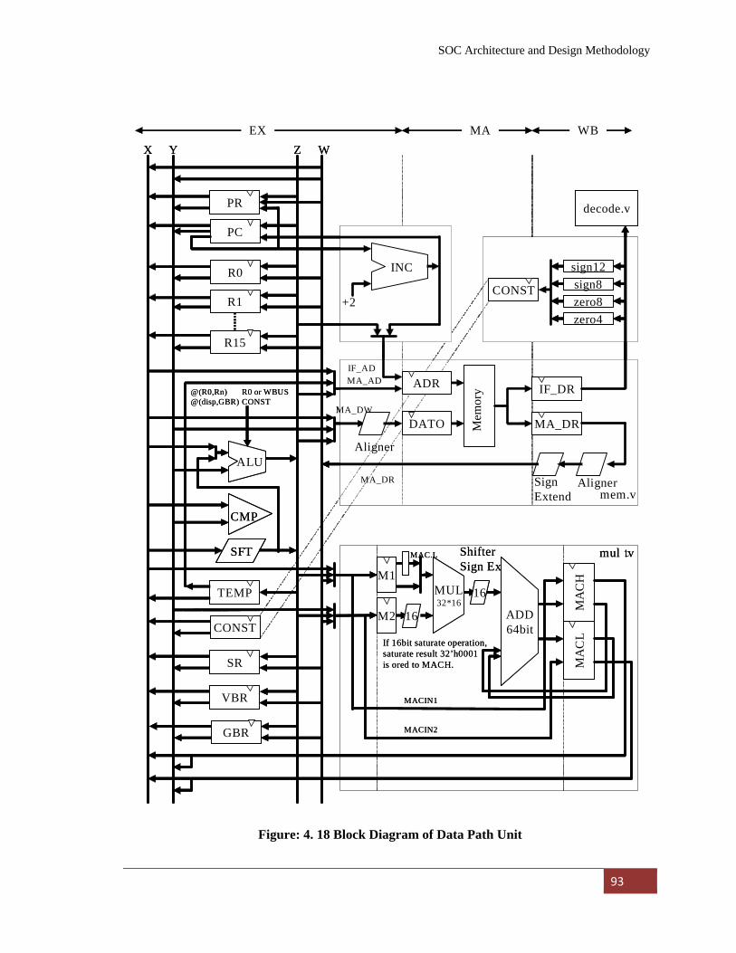
SOC Architecture and Design Methodology
93
16
R0
R1
X Y
R15
ALU
Z
ADR
DATO
Aligner
Mem
ory
MA_DR
AlignerSignExtend
EX MA WBW
M1
M2 ADD64bit
ShifterSign Ex
MA
CH
If 16bit saturate operation,saturate result 32’h0001is ored to MACH. M
AC
L16MUL
32*16
mem.v
mult.v
IF_ADMA_AD
MA_DW
IF_DR
MAC.L
MA_DR
PC
+2
INCsign8zero8zero4
sign12
decode.v
CONST
CONST
SR
VBR
PR
GBR
MACIN1
MACIN2
SFT
CMP
R0 or WBUSCONST
@(R0,Rn)@(disp,GBR)
TEMP
Figure: 4. 18 Block Diagram of Data Path Unit
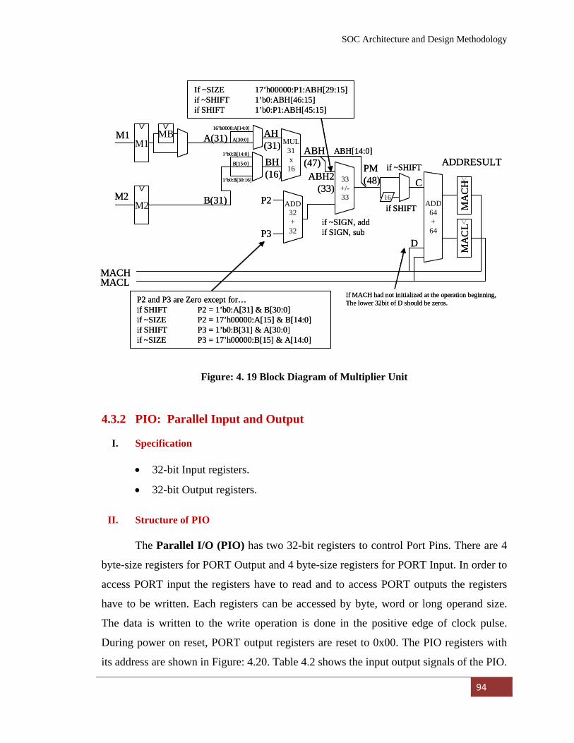
SOC Architecture and Design Methodology
94
MB A(31)
B(31)
B[15:0]
1’b0:B[30:16]
BH(16)
MUL31x
16
ADD64+64
16
MA
CH
MA
CL
MACHMACL
C
D
M1
M2
M1
M2
PM(48)
ADDRESULT
If MACH had not initialized at the operation beginning,The lower 32bit of D should be zeros.
33+/-33
ADD32+32
ABH(47)
P2
P3
P2 and P3 are Zero except for…if SHIFT P2 = 1’b0:A[31] & B[30:0] if ~SIZE P2 = 17’h00000:A[15] & B[14:0]if SHIFT P3 = 1’b0:B[31] & A[30:0]if ~SIZE P3 = 17’h00000:B[15] & A[14:0]
If ~SIZE 17’h00000:P1:ABH[29:15]if ~SHIFT 1’b0:ABH[46:15]if SHIFT 1’b0:P1:ABH[45:15]
if ~SIGN, addif SIGN, sub
ABH[14:0]
if SHIFT
if ~SHIFT
1’b0:B[14:0]
AH(31)
A[30:0]
16’h0000:A[14:0]
ABH2(33)
Figure: 4. 19 Block Diagram of Multiplier Unit
4.3.2 PIO: Parallel Input and Output
I. Specification
• 32-bit Input registers.
• 32-bit Output registers.
II. Structure of PIO
The Parallel I/O (PIO) has two 32-bit registers to control Port Pins. There are 4
byte-size registers for PORT Output and 4 byte-size registers for PORT Input. In order to
access PORT input the registers have to read and to access PORT outputs the registers
have to be written. Each registers can be accessed by byte, word or long operand size.
The data is written to the write operation is done in the positive edge of clock pulse.
During power on reset, PORT output registers are reset to 0x00. The PIO registers with
its address are shown in Figure: 4.20. Table 4.2 shows the input output signals of the PIO.
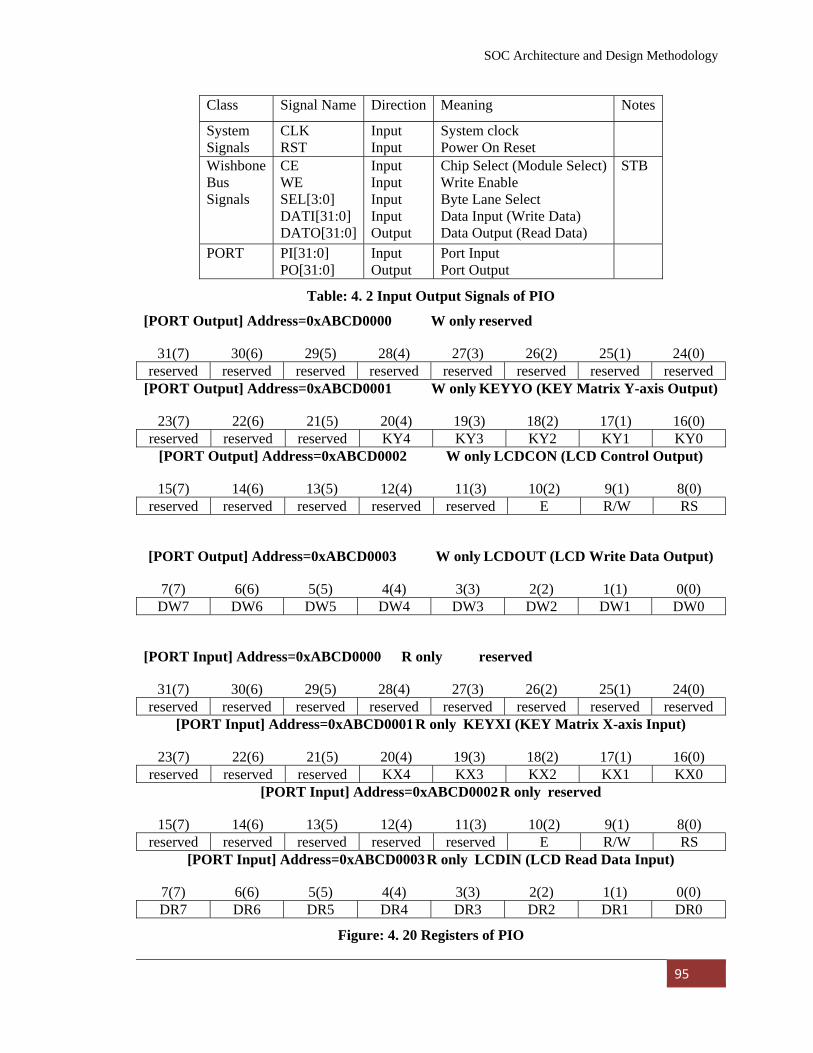
SOC Architecture and Design Methodology
95
Class Signal Name Direction Meaning Notes
System Signals
CLK RST
Input Input
System clock Power On Reset
Wishbone Bus Signals
CE WE SEL[3:0] DATI[31:0] DATO[31:0]
Input Input Input Input Output
Chip Select (Module Select) Write Enable Byte Lane Select Data Input (Write Data) Data Output (Read Data)
STB
PORT PI[31:0] PO[31:0]
Input Output
Port Input Port Output
Table: 4. 2 Input Output Signals of PIO
[PORT Output] Address=0xABCD0000 W only reserved
31(7) 30(6) 29(5) 28(4) 27(3) 26(2) 25(1) 24(0) reserved reserved reserved reserved reserved reserved reserved reserved
[PORT Output] Address=0xABCD0001 W only KEYYO (KEY Matrix Y-axis Output)
23(7) 22(6) 21(5) 20(4) 19(3) 18(2) 17(1) 16(0) reserved reserved reserved KY4 KY3 KY2 KY1 KY0
[PORT Output] Address=0xABCD0002 W only LCDCON (LCD Control Output)
15(7) 14(6) 13(5) 12(4) 11(3) 10(2) 9(1) 8(0) reserved reserved reserved reserved reserved E R/W RS
[PORT Output] Address=0xABCD0003 W only LCDOUT (LCD Write Data Output)
7(7) 6(6) 5(5) 4(4) 3(3) 2(2) 1(1) 0(0) DW7 DW6 DW5 DW4 DW3 DW2 DW1 DW0
[PORT Input] Address=0xABCD0000 R only reserved
31(7) 30(6) 29(5) 28(4) 27(3) 26(2) 25(1) 24(0) reserved reserved reserved reserved reserved reserved reserved reserved
[PORT Input] Address=0xABCD0001 R only KEYXI (KEY Matrix X-axis Input)
23(7) 22(6) 21(5) 20(4) 19(3) 18(2) 17(1) 16(0) reserved reserved reserved KX4 KX3 KX2 KX1 KX0
[PORT Input] Address=0xABCD0002 R only reserved
15(7) 14(6) 13(5) 12(4) 11(3) 10(2) 9(1) 8(0) reserved reserved reserved reserved reserved E R/W RS
[PORT Input] Address=0xABCD0003 R only LCDIN (LCD Read Data Input)
7(7) 6(6) 5(5) 4(4) 3(3) 2(2) 1(1) 0(0) DR7 DR6 DR5 DR4 DR3 DR2 DR1 DR0
Figure: 4. 20 Registers of PIO
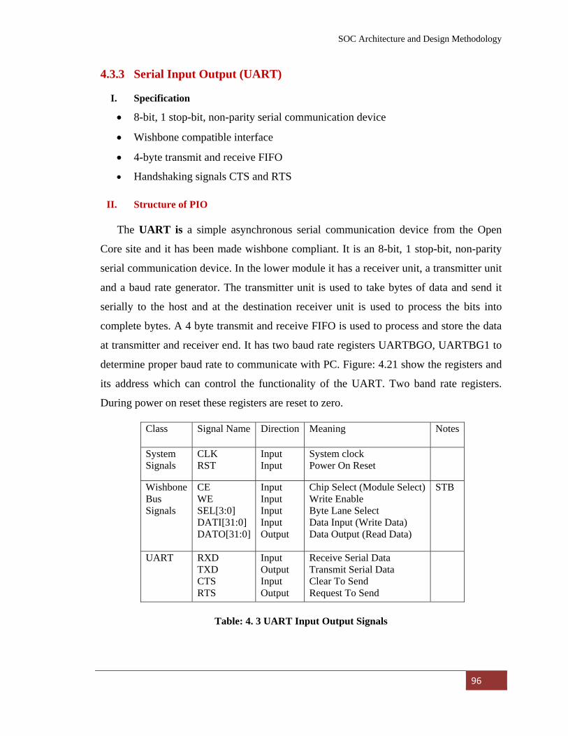
SOC Architecture and Design Methodology
96
4.3.3 Serial Input Output (UART)
I. Specification
• 8-bit, 1 stop-bit, non-parity serial communication device
• Wishbone compatible interface
• 4-byte transmit and receive FIFO
• Handshaking signals CTS and RTS
II. Structure of PIO
The UART is a simple asynchronous serial communication device from the Open
Core site and it has been made wishbone compliant. It is an 8-bit, 1 stop-bit, non-parity
serial communication device. In the lower module it has a receiver unit, a transmitter unit
and a baud rate generator. The transmitter unit is used to take bytes of data and send it
serially to the host and at the destination receiver unit is used to process the bits into
complete bytes. A 4 byte transmit and receive FIFO is used to process and store the data
at transmitter and receiver end. It has two baud rate registers UARTBGO, UARTBG1 to
determine proper baud rate to communicate with PC. Figure: 4.21 show the registers and
its address which can control the functionality of the UART. Two band rate registers.
During power on reset these registers are reset to zero.
Table: 4. 3 UART Input Output Signals
Class Signal Name Direction Meaning Notes
System Signals
CLK RST
Input Input
System clock Power On Reset
Wishbone Bus Signals
CE WE SEL[3:0] DATI[31:0] DATO[31:0]
Input Input Input Input Output
Chip Select (Module Select) Write Enable Byte Lane Select Data Input (Write Data) Data Output (Read Data)
STB
UART RXD TXD CTS RTS
Input Output Input Output
Receive Serial Data Transmit Serial Data Clear To Send Request To Send
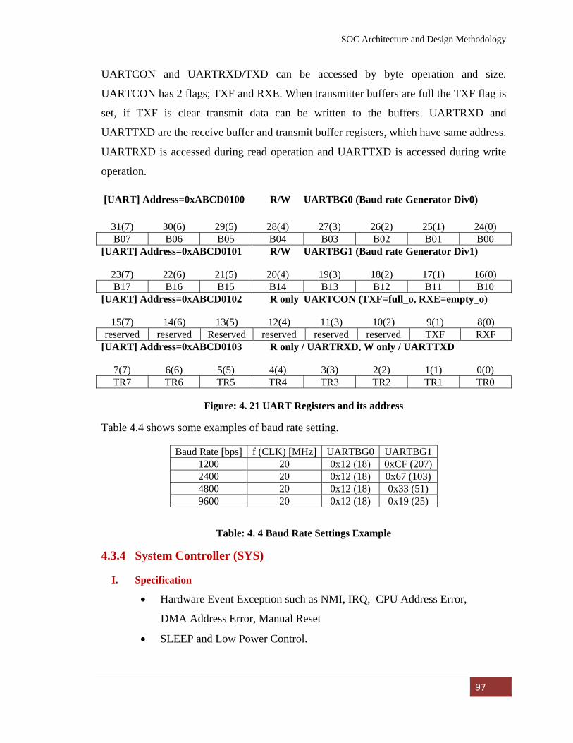
SOC Architecture and Design Methodology
97
UARTCON and UARTRXD/TXD can be accessed by byte operation and size.
UARTCON has 2 flags; TXF and RXE. When transmitter buffers are full the TXF flag is
set, if TXF is clear transmit data can be written to the buffers. UARTRXD and
UARTTXD are the receive buffer and transmit buffer registers, which have same address.
UARTRXD is accessed during read operation and UARTTXD is accessed during write
operation.
[UART] Address=0xABCD0100 R/W UARTBG0 (Baud rate Generator Div0)
31(7) 30(6) 29(5) 28(4) 27(3) 26(2) 25(1) 24(0) B07 B06 B05 B04 B03 B02 B01 B00
[UART] Address=0xABCD0101 R/W UARTBG1 (Baud rate Generator Div1)
23(7) 22(6) 21(5) 20(4) 19(3) 18(2) 17(1) 16(0) B17 B16 B15 B14 B13 B12 B11 B10
[UART] Address=0xABCD0102 R only UARTCON (TXF=full_o, RXE=empty_o)
15(7) 14(6) 13(5) 12(4) 11(3) 10(2) 9(1) 8(0) reserved reserved Reserved reserved reserved reserved TXF RXF
[UART] Address=0xABCD0103 R only / UARTRXD, W only / UARTTXD
7(7) 6(6) 5(5) 4(4) 3(3) 2(2) 1(1) 0(0) TR7 TR6 TR5 TR4 TR3 TR2 TR1 TR0
Figure: 4. 21 UART Registers and its address
Table 4.4 shows some examples of baud rate setting.
Baud Rate [bps] f (CLK) [MHz] UARTBG0 UARTBG1 1200 20 0x12 (18) 0xCF (207) 2400 20 0x12 (18) 0x67 (103) 4800 20 0x12 (18) 0x33 (51) 9600 20 0x12 (18) 0x19 (25)
Table: 4. 4 Baud Rate Settings Example
4.3.4 System Controller (SYS)
I. Specification
• Hardware Event Exception such as NMI, IRQ, CPU Address Error,
DMA Address Error, Manual Reset
• SLEEP and Low Power Control.
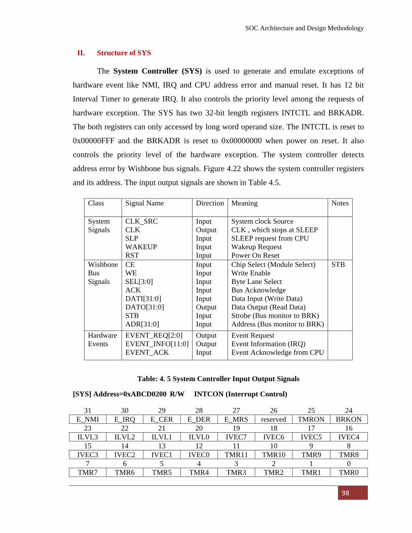
SOC Architecture and Design Methodology
98
II. Structure of SYS
The System Controller (SYS) is used to generate and emulate exceptions of
hardware event like NMI, IRQ and CPU address error and manual reset. It has 12 bit
Interval Timer to generate IRQ. It also controls the priority level among the requests of
hardware exception. The SYS has two 32-bit length registers INTCTL and BRKADR.
The both registers can only accessed by long word operand size. The INTCTL is reset to
0x00000FFF and the BRKADR is reset to 0x00000000 when power on reset. It also
controls the priority level of the hardware exception. The system controller detects
address error by Wishbone bus signals. Figure 4.22 shows the system controller registers
and its address. The input output signals are shown in Table 4.5.
Class Signal Name Direction Meaning Notes
System Signals
CLK_SRC CLK SLP WAKEUP RST
Input Output Input Input Input
System clock Source CLK , which stops at SLEEP SLEEP request from CPU Wakeup Request Power On Reset
Wishbone Bus Signals
CE WE SEL[3:0] ACK DATI[31:0] DATO[31:0] STB ADR[31:0]
Input Input Input Input Input Output Input Input
Chip Select (Module Select) Write Enable Byte Lane Select Bus Acknowledge Data Input (Write Data) Data Output (Read Data) Strobe (Bus monitor to BRK) Address (Bus monitor to BRK)
STB
Hardware Events
EVENT_REQ[2:0] EVENT_INFO[11:0] EVENT_ACK
Output Output Input
Event Request Event Information (IRQ) Event Acknowledge from CPU
Table: 4. 5 System Controller Input Output Signals
[SYS] Address=0xABCD0200 R/W INTCON (Interrupt Control)
31 30 29 28 27 26 25 24 E_NMI E_IRQ E_CER E_DER E_MRS reserved TMRON BRKON
23 22 21 20 19 18 17 16 ILVL3 ILVL2 ILVL1 ILVL0 IVEC7 IVEC6 IVEC5 IVEC4
15 14 13 12 11 10 9 8 IVEC3 IVEC2 IVEC1 IVEC0 TMR11 TMR10 TMR9 TMR8
7 6 5 4 3 2 1 0 TMR7 TMR6 TMR5 TMR4 TMR3 TMR2 TMR1 TMR0
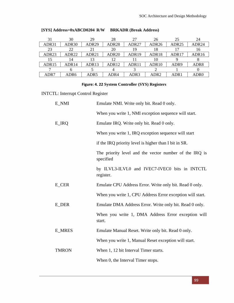
SOC Architecture and Design Methodology
99
[SYS] Address=0xABCD0204 R/W BRKADR (Break Address)
31 30 29 28 27 26 25 24 ADR31 ADR30 ADR29 ADR28 ADR27 ADR26 ADR25 ADR24
23 22 21 20 19 18 17 16 ADR23 ADR22 ADR21 ADR20 ADR19 ADR18 ADR17 ADR16
15 14 13 12 11 10 9 8 ADR15 ADR14 ADR13 ADR12 ADR11 ADR10 ADR9 ADR8
7 6 5 4 3 2 1 0 ADR7 ADR6 ADR5 ADR4 ADR3 ADR2 ADR1 ADR0
Figure: 4. 22 System Controller (SYS) Registers
INTCTL: Interrupt Control Register
E_NMI Emulate NMI. Write only bit. Read 0 only.
When you write 1, NMI exception sequence will start.
E_IRQ Emulate IRQ. Write only bit. Read 0 only.
When you write 1, IRQ exception sequence will start
if the IRQ priority level is higher than I bit in SR.
The priority level and the vector number of the IRQ is specified
by ILVL3-ILVL0 and IVEC7-IVEC0 bits in INTCTL register.
E_CER Emulate CPU Address Error. Write only bit. Read 0 only.
When you write 1, CPU Address Error exception will start.
E_DER Emulate DMA Address Error. Write only bit. Read 0 only.
When you write 1, DMA Address Error exception will start.
E_MRES Emulate Manual Reset. Write only bit. Read 0 only.
When you write 1, Manual Reset exception will start.
TMRON When 1, 12 bit Interval Timer starts.
When 0, the Interval Timer stops.
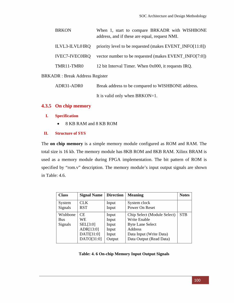
SOC Architecture and Design Methodology
100
BRKON When 1, start to compare BRKADR with WISHBONE address, and if these are equal, request NMI.
ILVL3-ILVL0 IRQ priority level to be requested (makes EVENT_INFO[11:8])
IVEC7-IVEC0 IRQ vector number to be requested (makes EVENT_INFO[7:0])
TMR11-TMR0 12 bit Interval Timer. When 0x000, it requests IRQ.
BRKADR : Break Address Register
ADR31-ADR0 Break address to be compared to WISHBONE address.
It is valid only when BRKON=1.
4.3.5 On chip memory
I. Specification
• 8 KB RAM and 8 KB ROM
II. Structure of SYS
The on chip memory is a simple memory module configured as ROM and RAM. The
total size is 16 kb. The memory module has 8KB ROM and 8KB RAM. Xilinx BRAM is
used as a memory module during FPGA implementation. The bit pattern of ROM is
specified by “rom.v” description. The memory module’s input output signals are shown
in Table: 4.6.
Class Signal Name Direction Meaning Notes
System Signals
CLK RST
Input Input
System clock Power On Reset
Wishbone Bus Signals
CE WE SEL[3:0] ADR[13:0] DATI[31:0] DATO[31:0]
Input Input Input Input Input Output
Chip Select (Module Select) Write Enable Byte Lane Select Address Data Input (Write Data) Data Output (Read Data)
STB
Table: 4. 6 On-chip Memory Input Output Signals
SOC Architecture and Design Methodology
101
4.4 Conclusions A SOC architecture proposed which consisting of 32-bit RISC CPU, UART, PIO,
System controller and on chip memory. These cores were collected from Open Core site.
A design methodology is described is used to implement this SOC architecture on FPGA.
The design methodology consists of hardware and software design flow. The hardware
design flow implement the SOC architecture into target FPGA. Software design flow is to
develop application program which can be ported in the system to verify the final
functionality of the system. Finally, the internal structures of the cores were discussed.
102
Integration of IP Cores
Verification of SOC
Synthesis results
FPGA Implementation
ChipScope Pro Result
Conclusions
Chapter 5
SOC Integration, Verification and FPGA Implementation
SOC Integration, Verification and FPGA Implementation
103
After defining the SOC architecture model and the design methodology to design
the SOC, the next step is to integrate all the IP cores to form the final architecture. The
steps of integrating the IP cores are described in this section. A test bench is used to
verify the top module of SOC using Xilinx ISE Simulator. A set of real time debugging
signals are presented to illustrate the internal architecture functionality of the SOC. The
steps involving FPGA implementation of the SOC architecture in Virtex–II Pro FPGA is
demonstrated. Finally, application codes are developed and ported on to SOC architecture
by a monitor program to observe, the SOC functionality.
5.1 Integration of IP Cores After the completion of both the hardware flow and the software flow, we obtained
a hardware model of SOC architecture. The next step is to implement the SOC model on
a target FPGA and to port application software on the SOC to verify the functionality of
the model. One of the most important tasks in this process is to integrate all the cores
collected. Hence there is a need of a top module HDL code which comprises a structural
modeling of the IP cores used for the implementation. All the Verilog files of the cores
are collected and a top module HDL code is written where Wishbone is the main
communicating interface between the IP cores and all the IP cores are interconnected
with the point to point interconnection. The 32-bit RISC CPU is the master for all the
components. All other component cores are configured as slaves to this master processor.
The integration process of point to point interconnection is easier than other types of
interconnection architectures described earlier. A set of steps has been considered for the
final integration is as follows:
1) Each slave component is defined by a specific address value. As the design uses a 32-
bit address space, the CPU can access the slaves by their respective addresses. To
implement this in the top module an address decoder is designed whose function is to
decode the address of slaves and enable the corresponding CE signal of the slave. As
described in the IN/OUT signals earlier, each slave is provided by a CE input signal
in the design. This helps in avoiding the address conflict and selecting the
corresponding slave according to the requirements. The peripheral devices are located
in 0xABCDxxxx area. The address map of the peripherals is shown in the Table: 5.1.
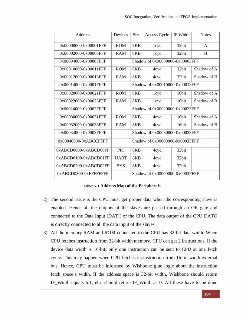
SOC Integration, Verification and FPGA Implementation
104
2) The second issue is the CPU must get proper data when the corresponding slave is
enabled. Hence all the outputs of the slaves are passed through an OR gate and
connected to the Data Input (DATI) of the CPU. The data output of the CPU DATO
is directly connected to all the data input of the slaves.
3) All the memory RAM and ROM connected to the CPU has 32-bit data width. When
CPU fetches instruction from 32-bit width memory, CPU can get 2 instructions. If the
device data width is 16-bit, only one instruction can be sent to CPU at one fetch
cycle. This may happen when CPU fetches its instruction from 16-bit width external
bus. Hence, CPU must be informed by Wishbone glue logic about the instruction
fetch space’s width. If the address space is 32-bit width, Wishbone should return
IF_Width equals to1, else should return IF_Width as 0. All these have to be done
Address Devices Size Access Cycle IF Width Notes
0x00000000-0x00001FFF ROM 8KB 1cyc 32bit A
0x00002000-0x00003FFF RAM 8KB 1cyc 32bit B
0x00004000-0x0000FFFF Shadow of 0x00000000-0x00003FFF
0x00010000-0x00011FFF ROM 8KB 4cyc 32bit Shadow of A
0x00012000-0x00013FFF RAM 8KB 4cyc 32bit Shadow of B
0x00014000-0x0001FFFF Shadow of 0x00010000-0x00013FFF
0x00020000-0x00021FFF ROM 8KB 1cyc 16bit Shadow of A
0x00022000-0x00023FFF RAM 8KB 1cyc 16bit Shadow of B
0x00024000-0x0002FFFF Shadow of 0x00020000-0x00023FFF
0x00030000-0x00031FFF ROM 8KB 4cyc 16bit Shadow of A
0x00032000-0x00033FFF RAM 8KB 4cyc 16bit Shadow of B
0x00034000-0x0003FFFF Shadow of 0x00030000-0x00033FFF
0x00040000-0xABCCFFFF Shadow of 0x00000000-0x0003FFFF
0xABCD0000-0xABCD00FF PIO 8KB 4cyc 32bit
0xABCD0100-0xABCD01FF UART 8KB 4cyc 32bit
0xABCD0200-0xABCD02FF SYS 8KB 4cyc 32bit
0xABCD0300-0xFFFFFFFF Shadow of 0x00000000-0x0003FFFF
Table: 5. 1 Address Map of the Peripherals
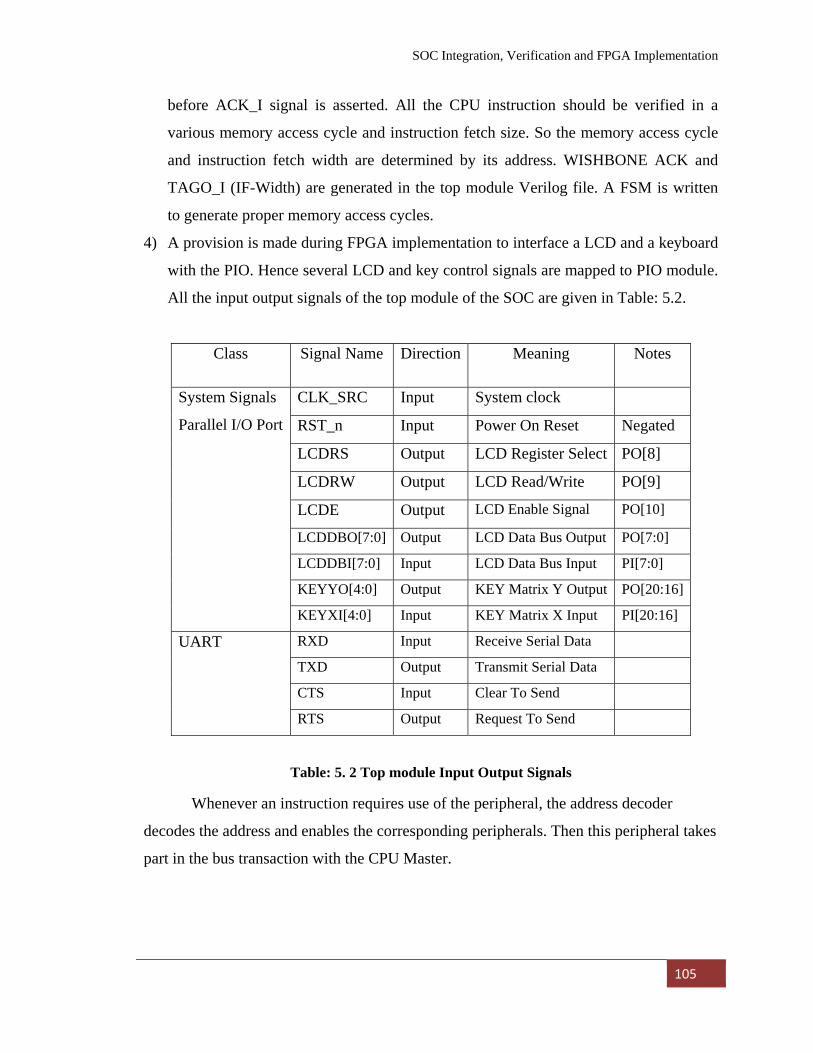
SOC Integration, Verification and FPGA Implementation
105
before ACK_I signal is asserted. All the CPU instruction should be verified in a
various memory access cycle and instruction fetch size. So the memory access cycle
and instruction fetch width are determined by its address. WISHBONE ACK and
TAGO_I (IF-Width) are generated in the top module Verilog file. A FSM is written
to generate proper memory access cycles.
4) A provision is made during FPGA implementation to interface a LCD and a keyboard
with the PIO. Hence several LCD and key control signals are mapped to PIO module.
All the input output signals of the top module of the SOC are given in Table: 5.2.
Class Signal Name Direction Meaning Notes
System Signals
Parallel I/O Port
CLK_SRC Input System clock
RST_n Input Power On Reset Negated
LCDRS Output LCD Register Select PO[8]
LCDRW Output LCD Read/Write PO[9]
LCDE Output LCD Enable Signal PO[10]
LCDDBO[7:0] Output LCD Data Bus Output PO[7:0]
LCDDBI[7:0] Input LCD Data Bus Input PI[7:0]
KEYYO[4:0] Output KEY Matrix Y Output PO[20:16]
KEYXI[4:0] Input KEY Matrix X Input PI[20:16]
UART RXD Input Receive Serial Data
TXD Output Transmit Serial Data
CTS Input Clear To Send
RTS Output Request To Send
Table: 5. 2 Top module Input Output Signals
Whenever an instruction requires use of the peripheral, the address decoder
decodes the address and enables the corresponding peripherals. Then this peripheral takes
part in the bus transaction with the CPU Master.
SOC Integration, Verification and FPGA Implementation
106
5.2 Verification of SOC A verification step plays an important role in SOC design flow. The peripheral
cores used are pre-verified cores, which function accurately. Hence, a test bench is
written in Verilog that verifies the CPU’s operation. The instructions of the CPU are
simulated considering bus transactions, signal levels and register contents, etc. This is
done by using an open source simulator Icarus Verilog [19].
5.2.1 Verification Environment
The environment used for verifying the instructions are described in this section.
The verification program and application program has been developed with the help of
GNU [24] assembler and C compiler for Super H-2. SuperH-2 assembler/compiler and
simulator for Verilog HDL runs on the UNIX environment. Hence Cygwin [21] is
selected as a preferred environment so that all the UNIX based tools can be operated in
windows platform. Hence the packages like GNU “Binutils”, “GCC”, “Newlib” and
“GDB” are downloaded and installed in the Cygwin environment. Three script files
“asm”, “sim”, “genrom” have been provided in the with the project in Open Core site. A
verification program is written which contains the CPU instructions. The S-Format object
file for this program is created by using “asm” script. After compiling the “genrom” file,
a “genrom” executable file is created which converts the S-Format object file to “rom.v”
file. The “rom.v” is the rom module which contains the CPU verification instructions.
After the “rom.v” file has been created the entire Verilog source file for CPU, UART,
SYS and PIO, integrated in a top module, and collected in the home directory of Cygwin
environment along with the script files and test bench file. Finally, with the help of “sim”
script simulation is accomplished using Icarus Verilog simulator. The writing of test-
bench and the outputs simulation are discussed in the next section.
5.2.2 Test Bench Development A test bench is a model which is used to verify the correctness of the design. It generally
consists of three parts. It generally consists of three parts:
• To Generate of stimulus for simulation
• To apply the stimulus to “design under test” (DUT), and
• To monitor the output and compare with the expected values.
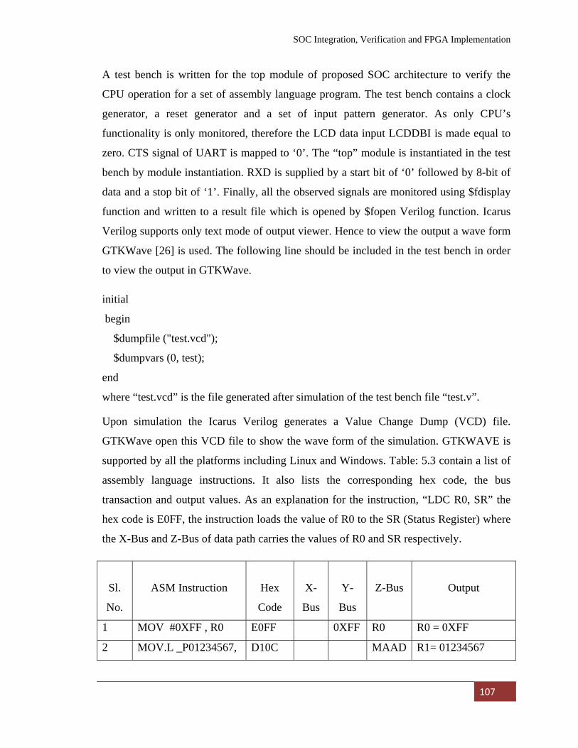
SOC Integration, Verification and FPGA Implementation
107
A test bench is written for the top module of proposed SOC architecture to verify the
CPU operation for a set of assembly language program. The test bench contains a clock
generator, a reset generator and a set of input pattern generator. As only CPU’s
functionality is only monitored, therefore the LCD data input LCDDBI is made equal to
zero. CTS signal of UART is mapped to ‘0’. The “top” module is instantiated in the test
bench by module instantiation. RXD is supplied by a start bit of ‘0’ followed by 8-bit of
data and a stop bit of ‘1’. Finally, all the observed signals are monitored using $fdisplay
function and written to a result file which is opened by $fopen Verilog function. Icarus
Verilog supports only text mode of output viewer. Hence to view the output a wave form
GTKWave [26] is used. The following line should be included in the test bench in order
to view the output in GTKWave.
initial
begin
$dumpfile ("test.vcd");
$dumpvars (0, test);
end
where “test.vcd” is the file generated after simulation of the test bench file “test.v”.
Upon simulation the Icarus Verilog generates a Value Change Dump (VCD) file.
GTKWave open this VCD file to show the wave form of the simulation. GTKWAVE is
supported by all the platforms including Linux and Windows. Table: 5.3 contain a list of
assembly language instructions. It also lists the corresponding hex code, the bus
transaction and output values. As an explanation for the instruction, “LDC R0, SR” the
hex code is E0FF, the instruction loads the value of R0 to the SR (Status Register) where
the X-Bus and Z-Bus of data path carries the values of R0 and SR respectively.
Sl.
No.
ASM Instruction
Hex
Code
X-
Bus
Y-
Bus
Z-Bus
Output
1 MOV #0XFF , R0 E0FF 0XFF R0 R0 = 0XFF
2 MOV.L _P01234567, D10C MAAD R1= 01234567
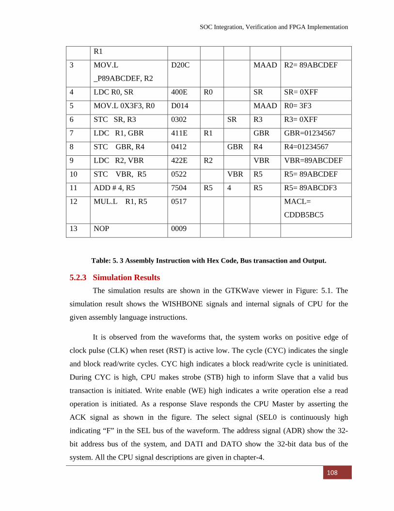
SOC Integration, Verification and FPGA Implementation
108
R1
3 MOV.L
_P89ABCDEF, R2
D20C MAAD R2= 89ABCDEF
4 LDC R0, SR 400E R0 SR SR= 0XFF
5 MOV.L 0X3F3, R0 D014 MAAD R0= 3F3
6 STC SR, R3 0302 SR R3 R3= 0XFF
7 LDC R1, GBR 411E R1 GBR GBR=01234567
8 STC GBR, R4 0412 GBR R4 R4=01234567
9 LDC R2, VBR 422E R2 VBR VBR=89ABCDEF
10 STC VBR, R5 0522 VBR R5 R5= 89ABCDEF
11 ADD # 4, R5 7504 R5 4 R5 R5= 89ABCDF3
12 MUL.L R1, R5 0517 MACL=
CDDB5BC5
13 NOP 0009
Table: 5. 3 Assembly Instruction with Hex Code, Bus transaction and Output.
5.2.3 Simulation Results The simulation results are shown in the GTKWave viewer in Figure: 5.1. The
simulation result shows the WISHBONE signals and internal signals of CPU for the
given assembly language instructions.
It is observed from the waveforms that, the system works on positive edge of
clock pulse (CLK) when reset (RST) is active low. The cycle (CYC) indicates the single
and block read/write cycles. CYC high indicates a block read/write cycle is uninitiated.
During CYC is high, CPU makes strobe (STB) high to inform Slave that a valid bus
transaction is initiated. Write enable (WE) high indicates a write operation else a read
operation is initiated. As a response Slave responds the CPU Master by asserting the
ACK signal as shown in the figure. The select signal (SEL0 is continuously high
indicating “F” in the SEL bus of the waveform. The address signal (ADR) show the 32-
bit address bus of the system, and DATI and DATO show the 32-bit data bus of the
system. All the CPU signal descriptions are given in chapter-4.
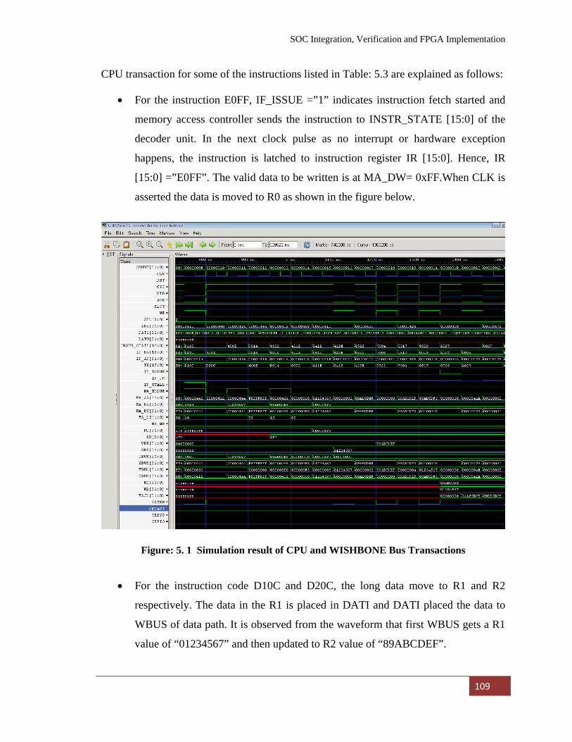
SOC Integration, Verification and FPGA Implementation
109
CPU transaction for some of the instructions listed in Table: 5.3 are explained as follows:
• For the instruction E0FF, IF_ISSUE =”1” indicates instruction fetch started and
memory access controller sends the instruction to INSTR_STATE [15:0] of the
decoder unit. In the next clock pulse as no interrupt or hardware exception
happens, the instruction is latched to instruction register IR [15:0]. Hence, IR
[15:0] =”E0FF”. The valid data to be written is at MA_DW= 0xFF.When CLK is
asserted the data is moved to R0 as shown in the figure below.
• For the instruction code D10C and D20C, the long data move to R1 and R2
respectively. The data in the R1 is placed in DATI and DATI placed the data to
WBUS of data path. It is observed from the waveform that first WBUS gets a R1
value of “01234567” and then updated to R2 value of “89ABCDEF”.
Figure: 5. 1 Simulation result of CPU and WISHBONE Bus Transactions
SOC Integration, Verification and FPGA Implementation
110
• Similarly for instruction code 411E, the value of R1 is loaded to GBR. The data
path uses Z-bus to contain the value of GBR and X-Bus to contain the value of R1
and we can see from the figure that after IR [15:0] = 411E, GBR updated with a
value of “01234567”.
• For the ADD instruction, the immediate value “4” is added to the content of R5.
During IR [15:0] = 7504 YBUS contain the immediate value “4” and XBUS
contains the old value of R5= “89ABCDEF”. After the instruction is completed
the value of R5 (XBUS) is incremented by “4” and gets updated to new value
“89ABCDF3”.
• For the MUL instruction R1 and R5 are multiplied. The R1 value from YBUS and
R5 value from XBUS are transferred to multiplier latch M1 and M2. Hence, M1=
“89ABCDF3” and M2=”01234567”. In the next clock pulse when ACK is high
M1 and M2 multiplied and the output register MACL contains the value of
“CDDB5BC5”.
• It is also observed that during when MA_ISSUE and IF_ISSUE are both high
(IF_MA conflict), memory access (MA) gets a priority than instruction fetch (IF).
In the final instruction “NOP” no operation is performed by the CPU.
• We can also observe that all the chip enable signal of peripherals such as, CEPIO,
CEUART, CESYS are low. The assertion in CEMEM indicates CPU memory
transactions are only taken place.
5.3 Synthesis results
One of the important steps in hardware design flow described earlier is synthesis
of the top module design. The synthesis is the process where RTL level code is converted
to real hardware. For this a synthesis tool is required. Xilinx XST is used to compile the
RTL behavior of the design to generate a gate level net list for the FPGA. Xilinx Virtex-
II pro FPGA is used as a platform for synthesis. The operating frequency is set as 20
MHz.
The synthesis has been done with taking constraints of minimum area and
maximum speed. Table: 5.4 and Table: 5.5 show the synthesis results of the designed
SOC with area and speed constraints. Table: 5.6 show the comparison of device
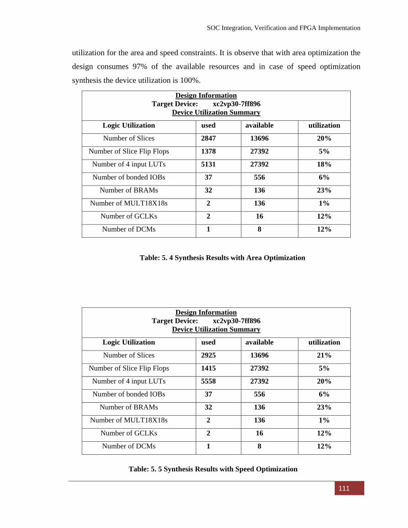
SOC Integration, Verification and FPGA Implementation
111
utilization for the area and speed constraints. It is observe that with area optimization the
design consumes 97% of the available resources and in case of speed optimization
synthesis the device utilization is 100%.
Design Information Target Device: xc2vp30-7ff896
Device Utilization Summary Logic Utilization used available utilization
Number of Slices 2847 13696 20%
Number of Slice Flip Flops 1378 27392 5%
Number of 4 input LUTs 5131 27392 18%
Number of bonded IOBs 37 556 6%
Number of BRAMs 32 136 23%
Number of MULT18X18s 2 136 1%
Number of GCLKs 2 16 12%
Number of DCMs 1 8 12%
Table: 5. 4 Synthesis Results with Area Optimization
Design Information Target Device: xc2vp30-7ff896
Device Utilization Summary Logic Utilization used available utilization
Number of Slices 2925 13696 21%
Number of Slice Flip Flops 1415 27392 5%
Number of 4 input LUTs 5558 27392 20%
Number of bonded IOBs 37 556 6%
Number of BRAMs 32 136 23%
Number of MULT18X18s 2 136 1%
Number of GCLKs 2 16 12%
Number of DCMs 1 8 12%
Table: 5. 5 Synthesis Results with Speed Optimization
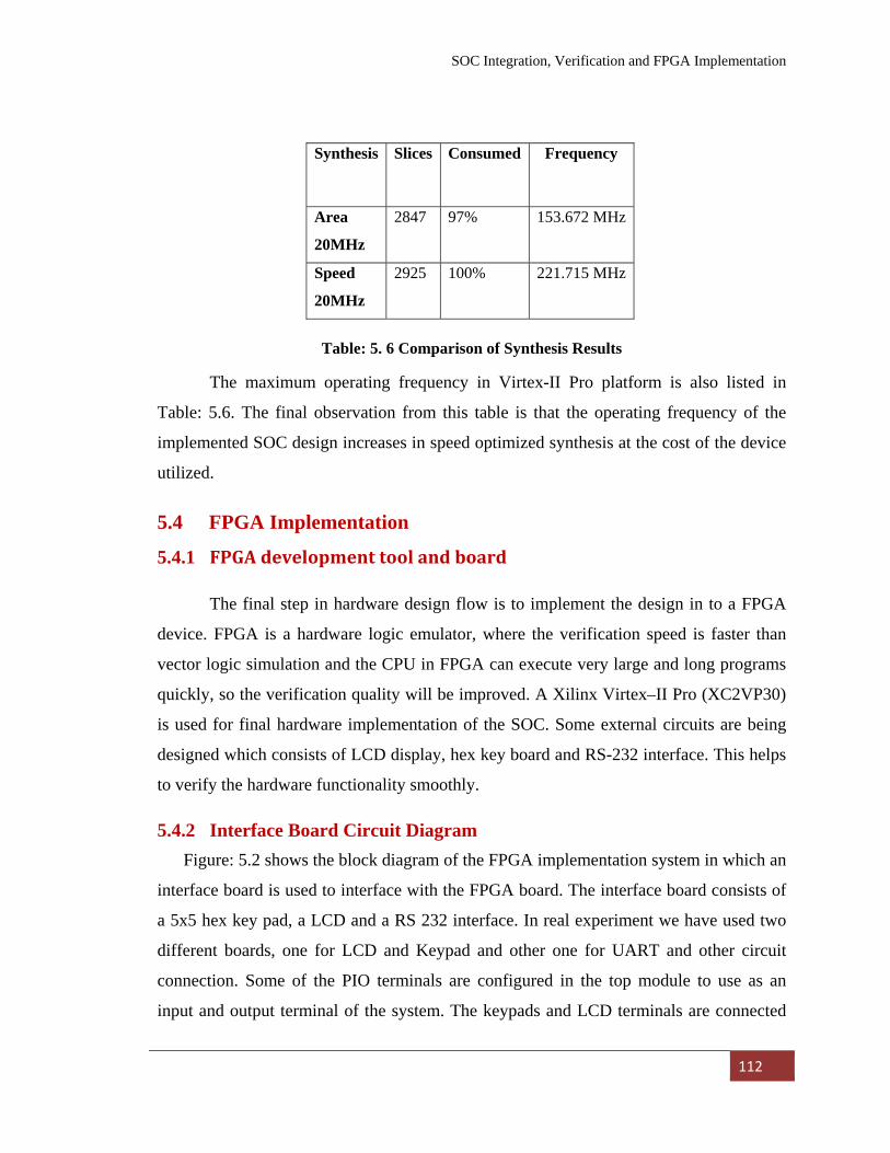
SOC Integration, Verification and FPGA Implementation
112
Table: 5. 6 Comparison of Synthesis Results
The maximum operating frequency in Virtex-II Pro platform is also listed in
Table: 5.6. The final observation from this table is that the operating frequency of the
implemented SOC design increases in speed optimized synthesis at the cost of the device
utilized.
5.4 FPGA Implementation
5.4.1 FPGA development tool and board
The final step in hardware design flow is to implement the design in to a FPGA
device. FPGA is a hardware logic emulator, where the verification speed is faster than
vector logic simulation and the CPU in FPGA can execute very large and long programs
quickly, so the verification quality will be improved. A Xilinx Virtex–II Pro (XC2VP30)
is used for final hardware implementation of the SOC. Some external circuits are being
designed which consists of LCD display, hex key board and RS-232 interface. This helps
to verify the hardware functionality smoothly.
5.4.2 Interface Board Circuit Diagram Figure: 5.2 shows the block diagram of the FPGA implementation system in which an
interface board is used to interface with the FPGA board. The interface board consists of
a 5x5 hex key pad, a LCD and a RS 232 interface. In real experiment we have used two
different boards, one for LCD and Keypad and other one for UART and other circuit
connection. Some of the PIO terminals are configured in the top module to use as an
input and output terminal of the system. The keypads and LCD terminals are connected
Synthesis Slices Consumed Frequency
Area
20MHz
2847 97% 153.672 MHz
Speed
20MHz
2925 100% 221.715 MHz
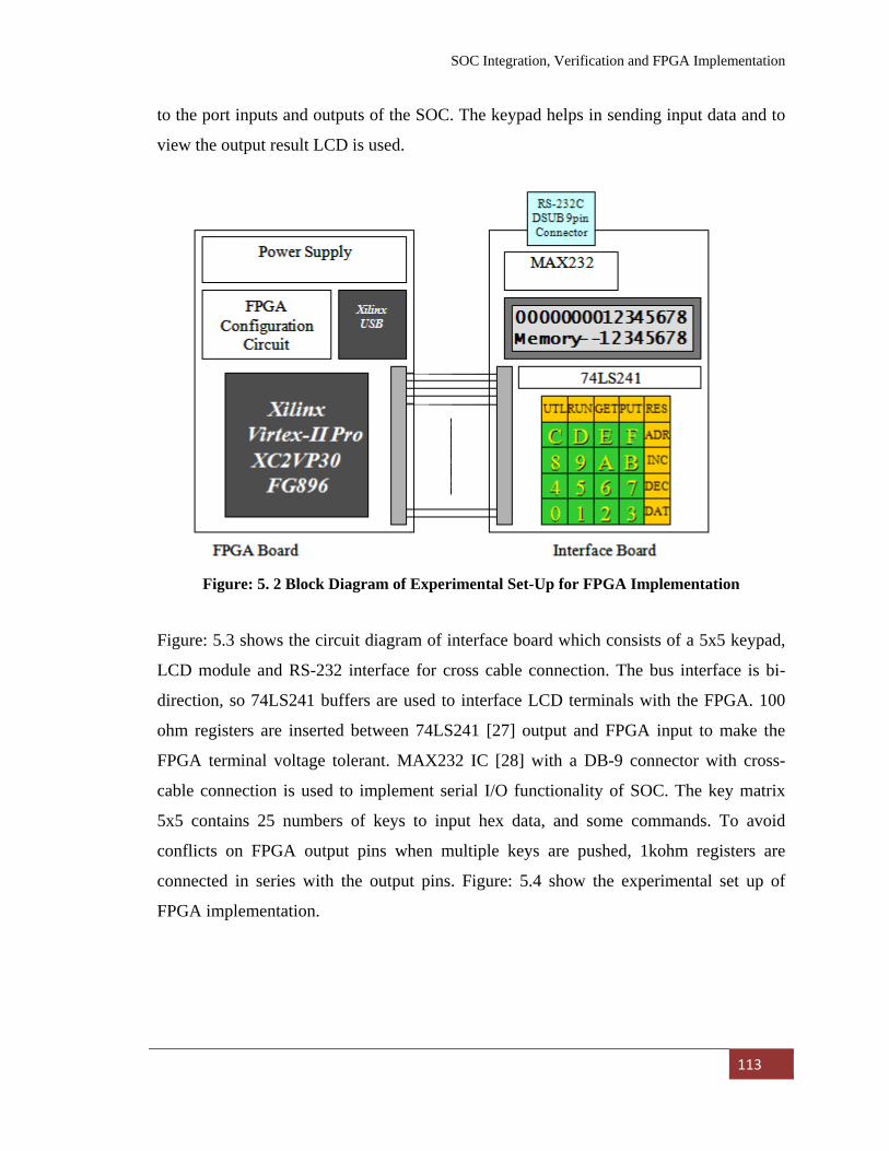
SOC Integration, Verification and FPGA Implementation
113
to the port inputs and outputs of the SOC. The keypad helps in sending input data and to
view the output result LCD is used.
Figure: 5. 2 Block Diagram of Experimental Set-Up for FPGA Implementation
Figure: 5.3 shows the circuit diagram of interface board which consists of a 5x5 keypad,
LCD module and RS-232 interface for cross cable connection. The bus interface is bi-
direction, so 74LS241 buffers are used to interface LCD terminals with the FPGA. 100
ohm registers are inserted between 74LS241 [27] output and FPGA input to make the
FPGA terminal voltage tolerant. MAX232 IC [28] with a DB-9 connector with cross-
cable connection is used to implement serial I/O functionality of SOC. The key matrix
5x5 contains 25 numbers of keys to input hex data, and some commands. To avoid
conflicts on FPGA output pins when multiple keys are pushed, 1kohm registers are
connected in series with the output pins. Figure: 5.4 show the experimental set up of
FPGA implementation.
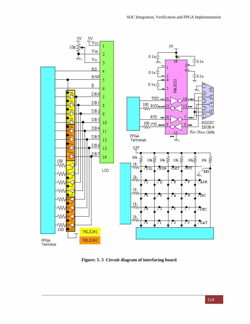
SOC Integration, Verification and FPGA Implementation
114
Figure: 5. 3 Circuit diagram of interfacing board
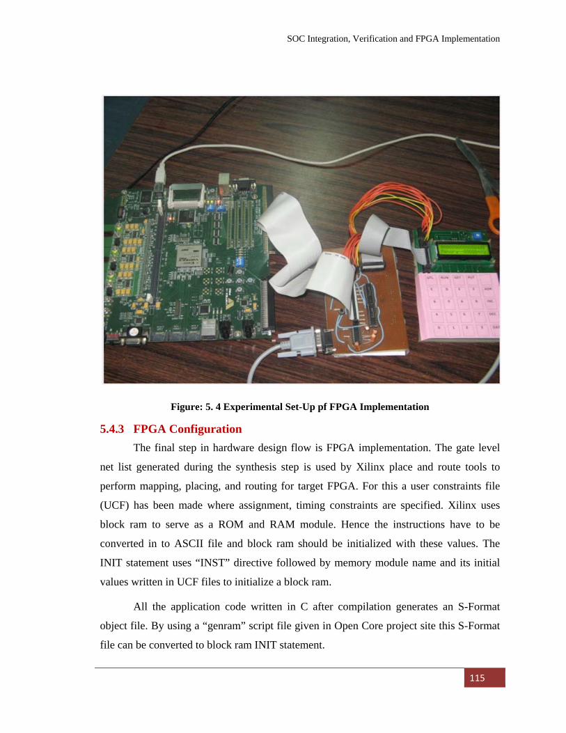
SOC Integration, Verification and FPGA Implementation
115
Figure: 5. 4 Experimental Set-Up pf FPGA Implementation
5.4.3 FPGA Configuration The final step in hardware design flow is FPGA implementation. The gate level
net list generated during the synthesis step is used by Xilinx place and route tools to
perform mapping, placing, and routing for target FPGA. For this a user constraints file
(UCF) has been made where assignment, timing constraints are specified. Xilinx uses
block ram to serve as a ROM and RAM module. Hence the instructions have to be
converted in to ASCII file and block ram should be initialized with these values. The
INIT statement uses “INST” directive followed by memory module name and its initial
values written in UCF files to initialize a block ram.
All the application code written in C after compilation generates an S-Format
object file. By using a “genram” script file given in Open Core project site this S-Format
file can be converted to block ram INIT statement.
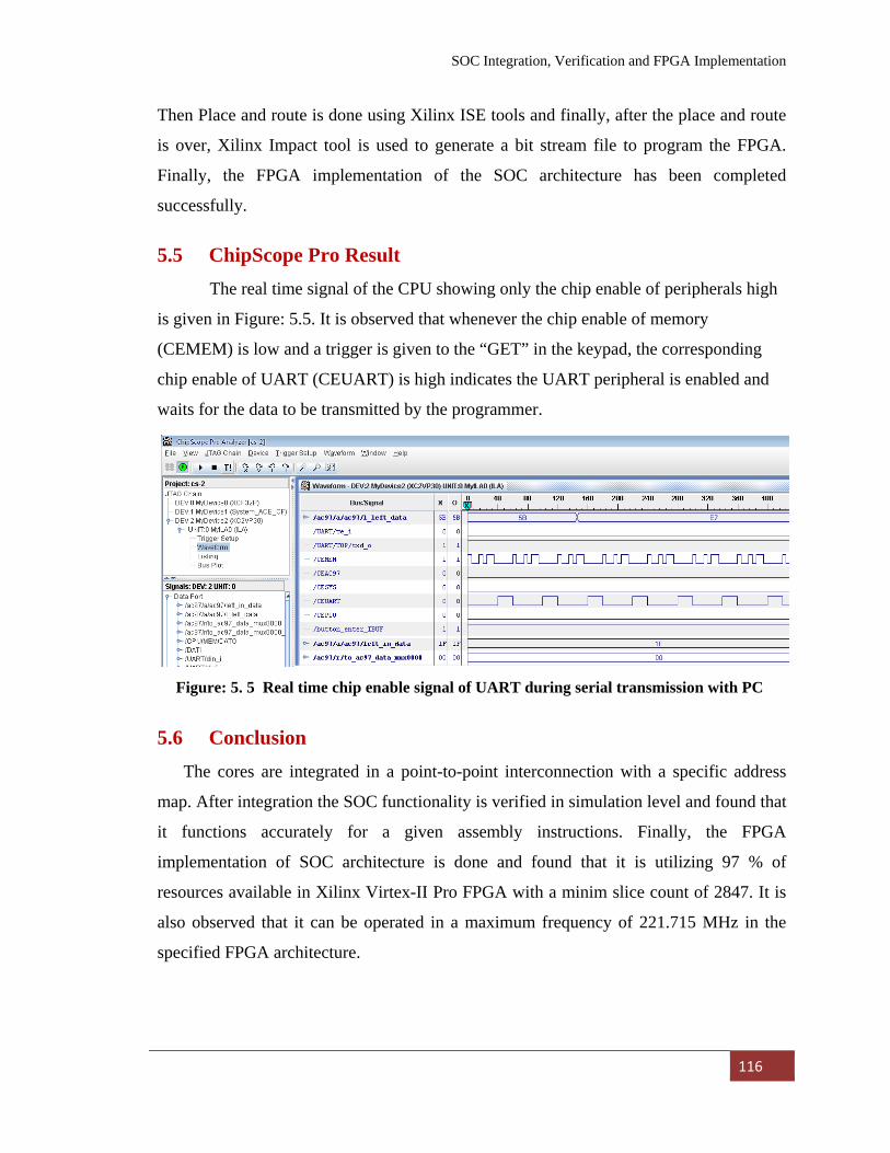
SOC Integration, Verification and FPGA Implementation
116
Then Place and route is done using Xilinx ISE tools and finally, after the place and route
is over, Xilinx Impact tool is used to generate a bit stream file to program the FPGA.
Finally, the FPGA implementation of the SOC architecture has been completed
successfully.
5.5 ChipScope Pro Result The real time signal of the CPU showing only the chip enable of peripherals high
is given in Figure: 5.5. It is observed that whenever the chip enable of memory
(CEMEM) is low and a trigger is given to the “GET” in the keypad, the corresponding
chip enable of UART (CEUART) is high indicates the UART peripheral is enabled and
waits for the data to be transmitted by the programmer.
5.6 Conclusion The cores are integrated in a point-to-point interconnection with a specific address
map. After integration the SOC functionality is verified in simulation level and found that
it functions accurately for a given assembly instructions. Finally, the FPGA
implementation of SOC architecture is done and found that it is utilizing 97 % of
resources available in Xilinx Virtex-II Pro FPGA with a minim slice count of 2847. It is
also observed that it can be operated in a maximum frequency of 221.715 MHz in the
specified FPGA architecture.
Figure: 5. 5 Real time chip enable signal of UART during serial transmission with PC
117
Application Programs
Monitor Program Application
Digital Clock Application
Audio Processing Application
Conclusions
Chapter 6
Application Development for SOC
Application Development for SOC Architecture
118
The final stage of SOC design flow is the real time functionality verification of
designed SOC architecture. A set of applications are developed in order to verify the
functionality. The application includes are monitor program, and clock application.
Finally, an AC97 WISHBONE compatible controller core is designed and integrated with
SOC for audio processing application.
6.1 Application Programs
One of the important flows in SOC design methodology is development of
application program which when loaded on the SOC architecture implemented in FPGA
performs some specific operations. The application program development requires a
software environment to develop it. Cygwin [21] is selected as the preferred environment
for this purpose. SuperH-2 assembler, compiler and debugger are used to build the
application program. Application program written in ‘C’ is compiled by GNU GCC [24]
and then debug by GNU GDB debugger. Finally by using monitor program provided by
Open Core the application is loaded in the SOC architecture and the functionality of SOC
is verified. The monitor program is converted to ASCII values and the values are written
to BRAM during FPGA implementation. Two programs written in C used for the
application development are
• Monitor program for memory editing and program loading.
• Timer application code for verification of functionality of the SOC.
While compiling the ‘C’ codes a start up program (crt0.s) and linker script (sh.x)
provided in Open Core project site is used along with a C complier header file files. A
make file is used to compile and link the C files.
6.2 Monitor Program Application
6.2.1 Algorithm for monitor program
The monitor program along with LCD display, keyboard and RS-232 interface
circuit performs debugging operation such as memory editor and program loader from PC
to SOC architecture. It also has additional capabilities like jumping to program and
debugging features such as setting of break point and reading registers. To write the
monitor program many functions are created in “C” and in a main program this functions
are called. Some of the functions are written below in the Table: 6.1.
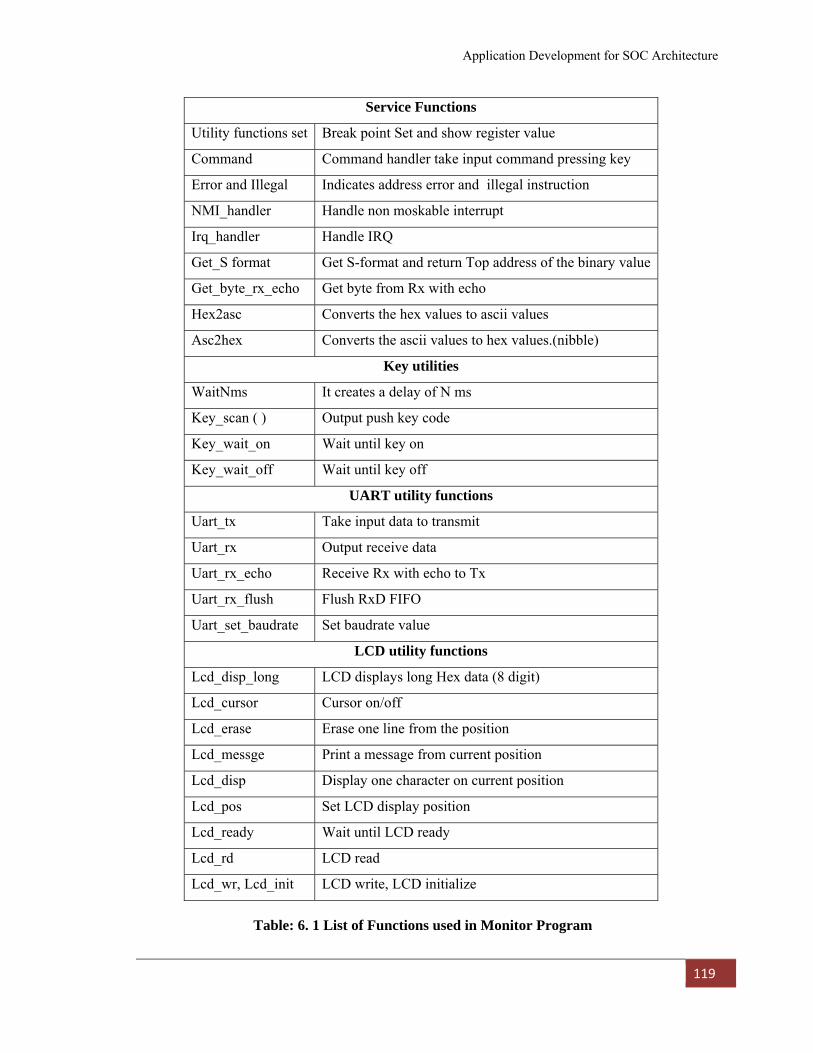
Application Development for SOC Architecture
119
Service Functions
Utility functions set Break point Set and show register value
Command Command handler take input command pressing key
Error and Illegal Indicates address error and illegal instruction
NMI_handler Handle non moskable interrupt
Irq_handler Handle IRQ
Get_S format Get S-format and return Top address of the binary value
Get_byte_rx_echo Get byte from Rx with echo
Hex2asc Converts the hex values to ascii values
Asc2hex Converts the ascii values to hex values.(nibble)
Key utilities
WaitNms It creates a delay of N ms
Key_scan ( ) Output push key code
Key_wait_on Wait until key on
Key_wait_off Wait until key off
UART utility functions
Uart_tx Take input data to transmit
Uart_rx Output receive data
Uart_rx_echo Receive Rx with echo to Tx
Uart_rx_flush Flush RxD FIFO
Uart_set_baudrate Set baudrate value
LCD utility functions
Lcd_disp_long LCD displays long Hex data (8 digit)
Lcd_cursor Cursor on/off
Lcd_erase Erase one line from the position
Lcd_messge Print a message from current position
Lcd_disp Display one character on current position
Lcd_pos Set LCD display position
Lcd_ready Wait until LCD ready
Lcd_rd LCD read
Lcd_wr, Lcd_init LCD write, LCD initialize
Table: 6. 1 List of Functions used in Monitor Program
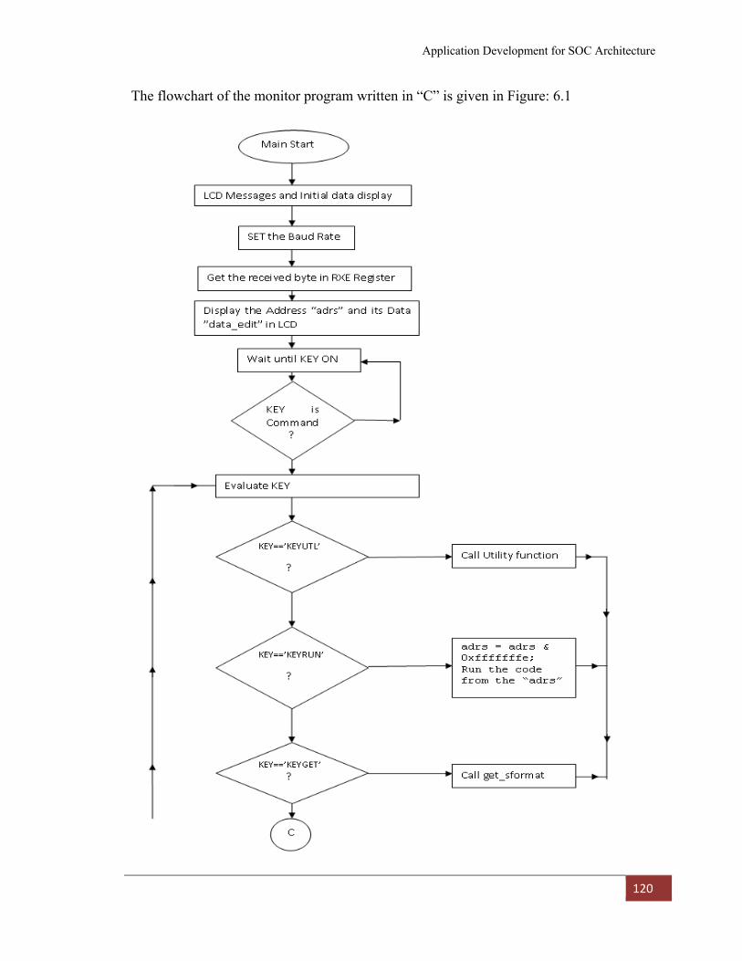
Application Development for SOC Architecture
120
The flowchart of the monitor program written in “C” is given in Figure: 6.1
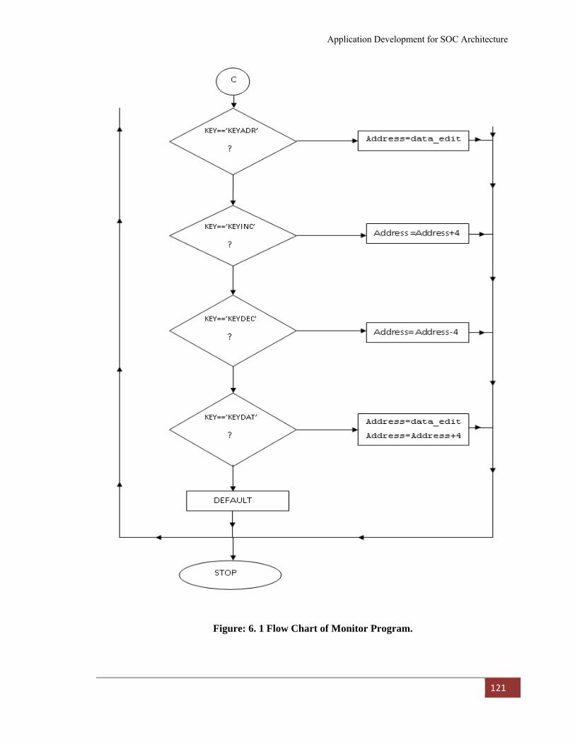
Application Development for SOC Architecture
121
Figure: 6. 1 Flow Chart of Monitor Program.

Application Development for SOC Architecture
122
6.2.2 How Monitor Program Works
The working procedure of how the monitor program works in real time environment is
described as follows. The corresponding LCD outputs in pictorial form are presented in
Figure: 6.2.
A. Memory editor:
a. Power On Reset (Start Up):
It shows a long-word sized data in the LCD. In the top line the left 8 hex numbers
shows memory address and right 8 hex numbers shows the data at this addresses.
b. Increment Address:
The “INC” key on the hex key pad increases the address by 4-byte and the
corresponding data at this address appears at the right side hex numbers.
c. Decrement Address:
The “DEC” key on the key pad decreases the address by ‐4‐byte, and the
corresponding data at this address appears at the right side hex numbers.
d. Enter And Set Address:
In order to view a data at other address location, enter a 4-byte address at the
bottom and push “ADR” key and the data will appear at the right side of the
top line. If address entered is not multiple of 4, the lower 2-bits of address are
cleared to 0, to avoid address error.
e. Enter And Write Data:
In order to change the data displayed in an address location, enter the new
data at the bottom line and press “DAT” key will update the new data and
increases the address by 4-byte. To verify the data written press “DEC” key.
B. Program Loader.
f. Program Loading From PC
g. Loading
h. Finish Loading
The S-Format (S3) object file can be downloaded to PC via RS-232 interface. The
default baud rate used for this is 1200 bps. The baud rate can be changed by changing
UARTBG0 and UARTBG1 register values in monitor program. The S-Format
records comprises S0 (comment), S3 (actual object), and S7 (end of record). By using

Application Development for SOC Architecture
123
the Makefile and “asm” script file the S-Format file can be generated. Pressing
“GET” key in the key pad, the FPGA system waits for sending data. The data can be
sent to FPGA by using hyper terminal application of PC. During the transfer of
objects the top address of every record is shown in the LCD. If any check sum error is
found by the monitor, the transfer will stop. When S7 is received by the monitor, the
program loading is stopped.
C. Run
i. Target Address Set And Goes To Program
j. Running Program
An application code for LCD display is developed and the S-Format file is loaded to
the FPGA system. This program is located at 0x00003000 (vector table present here)
and to start the program jump to the actual address 0x00003008 by pressing “ADR”
key. To start running the program “RUN” button is used and the LCD displays some
preset characters such as “SOC @ NIT RKL”. “RST” is used to make the system
power on reset.
D. Debug Utility
k. Select Register Reading And Check All CPU Registers
Pressing “UTL” and “1” key all register content can be checked.
l. Enter Break Address
Pressing “UTL” key and “2” and the break address from the key pad t
m. Set Break Point, Try A Break,
n. Break Happens.
Pressing ‘UTL’ key and entering “2” and the break address from the key pad can
be sent to the FPGA system. Then pressing DAT confirms the break operation. If
a value 0x00003800 is set as break point, then accessing 0x00003800 monitor
reports BRK has happened.
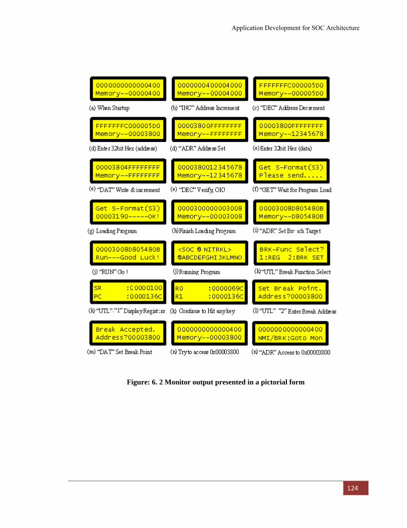
Application Development for SOC Architecture
124
Figure: 6. 2 Monitor output presented in a pictorial form
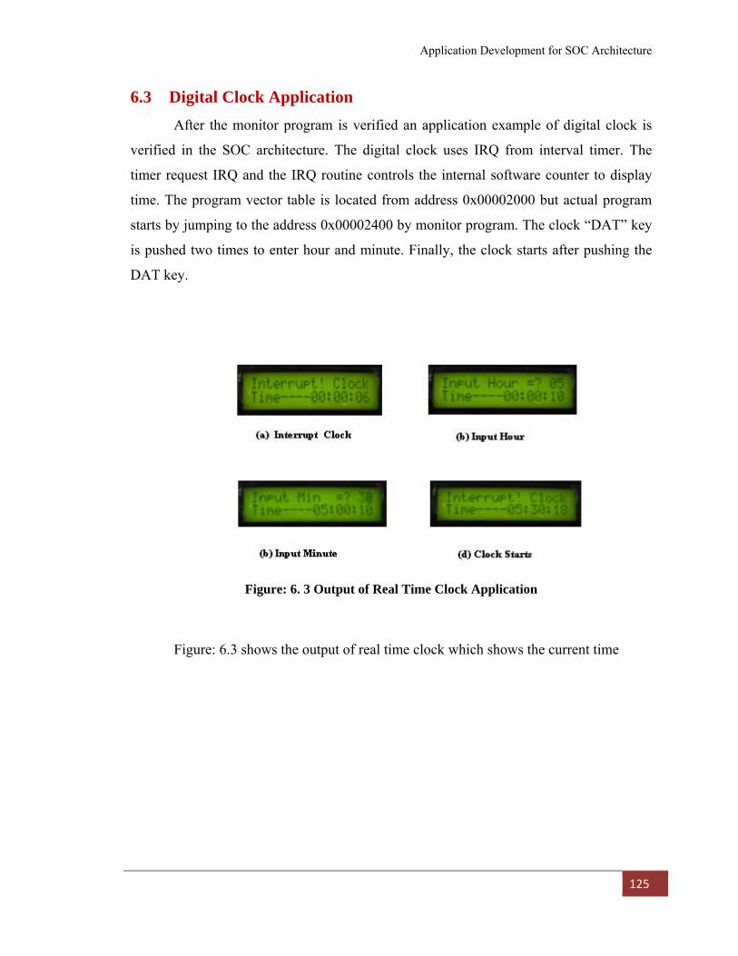
Application Development for SOC Architecture
125
6.3 Digital Clock Application After the monitor program is verified an application example of digital clock is
verified in the SOC architecture. The digital clock uses IRQ from interval timer. The
timer request IRQ and the IRQ routine controls the internal software counter to display
time. The program vector table is located from address 0x00002000 but actual program
starts by jumping to the address 0x00002400 by monitor program. The clock “DAT” key
is pushed two times to enter hour and minute. Finally, the clock starts after pushing the
DAT key.
Figure: 6. 3 Output of Real Time Clock Application
Figure: 6.3 shows the output of real time clock which shows the current time
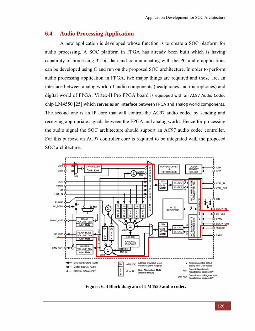
Application Development for SOC Architecture
126
6.4 Audio Processing Application A new application is developed whose function is to create a SOC platform for
audio processing. A SOC platform in FPGA has already been built which is having
capability of processing 32-bit data and communicating with the PC and e applications
can be developed using C and run on the proposed SOC architecture. In order to perform
audio processing application in FPGA, two major things are required and those are, an
interface between analog world of audio components (headphones and microphones) and
digital world of FPGA. Virtex-II Pro FPGA board is equipped with an AC97 Audio Codec
chip LM4550 [25] which serves as an interface between FPGA and analog world components.
The second one is an IP core that will control the AC97 audio codec by sending and
receiving appropriate signals between the FPGA and analog world. Hence for processing
the audio signal the SOC architecture should support an AC97 audio codec controller.
For this purpose an AC97 controller core is required to be integrated with the proposed
SOC architecture.
Figure: 6. 4 Block diagram of LM4550 audio codec.
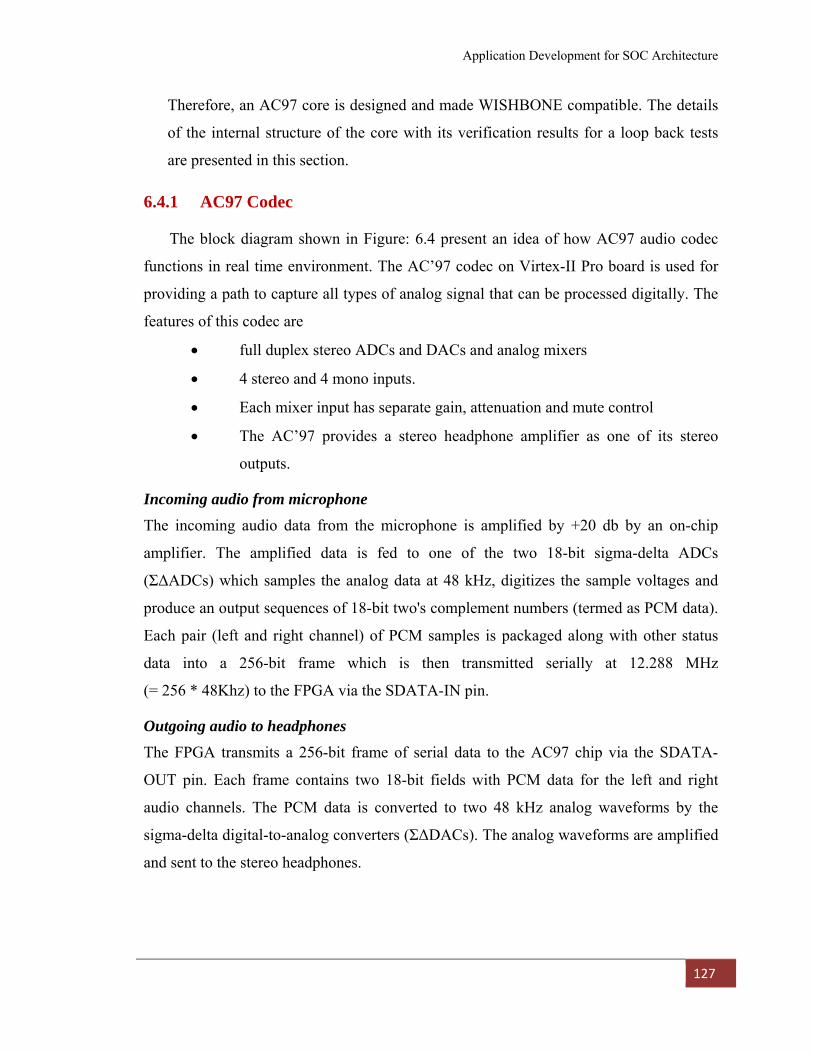
Application Development for SOC Architecture
127
Therefore, an AC97 core is designed and made WISHBONE compatible. The details
of the internal structure of the core with its verification results for a loop back tests
are presented in this section.
6.4.1 AC97 Codec
The block diagram shown in Figure: 6.4 present an idea of how AC97 audio codec
functions in real time environment. The AC’97 codec on Virtex-II Pro board is used for
providing a path to capture all types of analog signal that can be processed digitally. The
features of this codec are
• full duplex stereo ADCs and DACs and analog mixers
• 4 stereo and 4 mono inputs.
• Each mixer input has separate gain, attenuation and mute control
• The AC’97 provides a stereo headphone amplifier as one of its stereo
outputs.
Incoming audio from microphone The incoming audio data from the microphone is amplified by +20 db by an on-chip
amplifier. The amplified data is fed to one of the two 18-bit sigma-delta ADCs
(ΣΔADCs) which samples the analog data at 48 kHz, digitizes the sample voltages and
produce an output sequences of 18-bit two's complement numbers (termed as PCM data).
Each pair (left and right channel) of PCM samples is packaged along with other status
data into a 256-bit frame which is then transmitted serially at 12.288 MHz
(= 256 * 48Khz) to the FPGA via the SDATA-IN pin.
Outgoing audio to headphones The FPGA transmits a 256-bit frame of serial data to the AC97 chip via the SDATA-
OUT pin. Each frame contains two 18-bit fields with PCM data for the left and right
audio channels. The PCM data is converted to two 48 kHz analog waveforms by the
sigma-delta digital-to-analog converters (ΣΔDACs). The analog waveforms are amplified
and sent to the stereo headphones.
Application Development for SOC Architecture
128
Figure: 6.5 shows the AC link serial interface protocol where SDATA_OUT and
SDATA_IN signal carries AC link outgoing frames and AC link incoming frames
respectively. SDATA_IN is an output signal from the AC97 controller and input to the
codec. Output frames are consists of one Tag SLOT and twelve data SLOTs. Output
frame starts with a low-to-high transition of SYNC which should be clocked from the
controller on a rising edge of BIT_CLK (not shown in the figure).Each frame consists of
256-bits with each of the twelve data SLOTs containing 20-bits. The first bit of SLOT 0
is designated as “valid frame”. If this bit is 1, it indicates that the current output frame
contains at least one slot of valid data and the codec will check further tag bits for valid
data in the expected data SLOTs. SLOT 1 is used by a controller to indicate both the
address of a target register in the codec and whether the access operation is register read
or register write. SLOT 2 is used to transmit 16-bit control data to the codec when the
access operation is “write”. SLOTs 3 and 4 are 20-bit fields used to transmit PCM data
to the left and right channels of the stereo DAC when the codec is in Primary mode or
Secondary mode 1. SLOTs 7 and 8 are 20-bit fields used to transmit PCM data to the left
and right channels of the stereo DAC when the codec is in Secondary mode 2. Any
unused bits should be stuffed with zeros. SLOTs 6 and 9 are 20-bit fields used to
transmit PCM data to the left and right channels of the stereo DAC when the codec is in
Secondary mode 3. Any unused bits should be stuffed with zeros. SLOTs 5, 10, 11, 12
are reserved SLOTs, are not used by the codec and should all be stuffed with zeros by
the AC97 Controller.
Figure: 6. 5 AC link serial interface protocol
Application Development for SOC Architecture
129
SDATA_IN signal is an input to the AC97 Digital Audio Controller and an output from
the codec. Input Frames consists of one Tag SLOT followed by twelve Data SLOTs.
SLOT 1 echoes (in bits 18 – 12) the 7-bit address of the codec control/status register
received from the controller as part of a read-request in the previous frame. By default,
data is requested in every frame, corresponding to a sample rate equal to the frame rate
(SYNC frequency) – 48 kHz when XTAL_IN = 24.576 MHz.
The SLOT 2 returns 16-bit status data read from a codec control/ status register.
The codec sends the data in the frame following a read-request by the controller. This
SLOT 3 and SLOT 4 contain sampled data from the left and right channel of the stereo
ADC. The signal to be digitized is selected using the Record Select register (1Ah) and
subsequently routed through the Record Select Multiplexer and the Record Gain
amplifier to the ADC. This is a 20-bit SLOT and the digitized 18-bit PCM data is
transmitted in MSB justified format. The remaining 2 LSBs are stuffed with zeros. Slots
5-12 of the AC Link Input Frame are reserved slot not used for data by the codec and are
always stuffed with zeros.
6.4.2 Wishbone compatible AC97 Controller core design and Verification AC97 codec follows the AC serial link protocol to send or receive the PCM data.
Therefore, an AC97 controller core is required to keep up with the codec's data rates.
With considering these design criteria, AC97 controller is being designed that has the
following components:
Top: This module is the top module that includes instances of the AC97_top and recorder
blocks. This also has the WISHBONE bus interface.
AC97_Top: This block is a wrapper around the AC97_interface and AC97_commands.
This module has three ports: a ready output which indicates that a new sample is ready,
and two 8-bit data ports, one for incoming PCM data and one for outgoing PCM data.
AC97_Interface: This block has ports for incoming and outgoing 18-bit stereo PCM data.
It provides interface to the AC97 codec and transmit and receive the 256-bit serial data
streams.
AC97_Commands: This block generates commands to write to the AC97 command
registers for performing the appropriate initialization. The various commands are
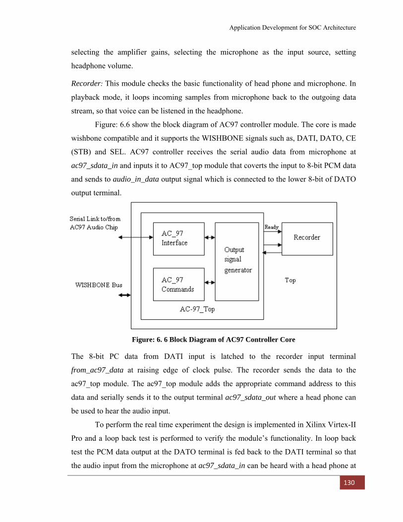
Application Development for SOC Architecture
130
selecting the amplifier gains, selecting the microphone as the input source, setting
headphone volume.
Recorder: This module checks the basic functionality of head phone and microphone. In
playback mode, it loops incoming samples from microphone back to the outgoing data
stream, so that voice can be listened in the headphone.
Figure: 6.6 show the block diagram of AC97 controller module. The core is made
wishbone compatible and it supports the WISHBONE signals such as, DATI, DATO, CE
(STB) and SEL. AC97 controller receives the serial audio data from microphone at
ac97_sdata_in and inputs it to AC97_top module that coverts the input to 8-bit PCM data
and sends to audio_in_data output signal which is connected to the lower 8-bit of DATO
output terminal.
Figure: 6. 6 Block Diagram of AC97 Controller Core
The 8-bit PC data from DATI input is latched to the recorder input terminal
from_ac97_data at raising edge of clock pulse. The recorder sends the data to the
ac97_top module. The ac97_top module adds the appropriate command address to this
data and serially sends it to the output terminal ac97_sdata_out where a head phone can
be used to hear the audio input.
To perform the real time experiment the design is implemented in Xilinx Virtex-II
Pro and a loop back test is performed to verify the module’s functionality. In loop back
test the PCM data output at the DATO terminal is fed back to the DATI terminal so that
the audio input from the microphone at ac97_sdata_in can be heard with a head phone at
Application Development for SOC Architecture
131
ac97_sdata_out. The verification of the functionally of the core for loop back test is
observed using Xilinx ChipScope Pro tools.
Figure: 6.7 shows the real time signals of the loop back test performed. The audio signal
at ac97_sdata_in is converted to 8-bit PCM data by A97_Top module and available at
left_in_data which is again latched to the input of the recorder module at the rising edge
of clock pulse. During playback mode the recorder module the data is routed to the
to_ac97_data_mux0000 terminal of AC97_Top module. AC97_Top module adds the
PCM data with appropriate command address and the audio signal can available for
hearing at ac97_sdata_out. Hence it is observed from the figure that the data input and
output are same set of PCM data.
Figure: 6. 7 real time signals of AC 97 Controller for the loop back test performed
Figure: 6. 8 SOC Architecture for Audio Processing Application
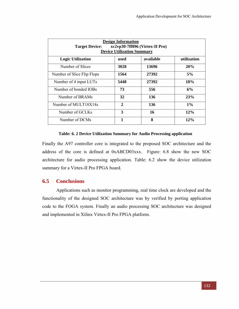
Application Development for SOC Architecture
132
Finally the A97 controller core is integrated to the proposed SOC architecture and the
address of the core is defined at 0xABCD03xxx. Figure: 6.8 show the new SOC
architecture for audio processing application. Table: 6.2 show the device utilization
summary for a Virtex-II Pro FPGA board.
6.5 Conclusions Applications such as monitor programming, real time clock are developed and the
functionality of the designed SOC architecture was by verified by porting application
code to the FOGA system. Finally an audio processing SOC architecture was designed
and implemented in Xilinx Virtex-II Pro FPGA platform.
Table: 6. 2 Device Utilization Summary for Audio Processing application
Design Information Target Device: xc2vp30-7ff896 (Virtex-II Pro)
Device Utilization Summary Logic Utilization used available utilization
Number of Slices 3028 13696 20%
Number of Slice Flip Flops 1564 27392 5%
Number of 4 input LUTs 5448 27392 18%
Number of bonded IOBs 73 556 6%
Number of BRAMs 32 136 23%
Number of MULT18X18s 2 136 1%
Number of GCLKs 3 16 12%
Number of DCMs 1 8 12%
Conclusions
Scope for Future Work
Chapter 7
Conclusions
133
7.1 Conclusions The recent advances in silicon technology now enable new levels of system
integration onto a single chip and allow building of chips consisting of millions of
transistors. With the evolution of technology and the increase in demands of more
powerful products System-on-chip (SOC) design has moved from leading edge to main-
stream design practice. Hence, there is a need of SOC design methodologies that are
reliable and requires shorter time to market. After a complete literature survey we
observe that “Design-reuse” is the key factor behind SOC design. This thesis investigated
two design methodologies such as PBD and open core based SOC design methodology.
PBD design is an emerging technology that utilizes previously design platform of
abstraction level to design the SOC, but it requires a library of platform which can only
be possible in industry environment. On the other hand open core SOC design utilizes
standard WISHBONE bus interface for design reuse and help in plug and play integration
of freely available IP cores to produce low cost, reliable, time-to-market SOC design.
The complete Wishbone literature has been reviewed and compared with two standard
bus interface AMBA and CoreConnect and the following conclusions are made:
• It is a standard interface available freely and can be used SOC integration without
any additional cost.
• It supports variable interconnection and variable time-specification.
• It supports single Read/Write; block Read/Write bus cycles. It also supports
RMW cycle as compared to split transaction of AMBA and core connect to share
memory used in multiprocessor SOC environment.
• It can be coded using any hardware description language like VHDL and Verilog
and for implementation it takes simple logic gates supported by most of the
FPGA and ASIC devices.
Two small system designs have been developed using both point-to-point and share-bus
interconnections. The issues related to design and integration of point-to-point and shared
bus interconnections are discussed and verification of the designs has been done using
Xilinx ISE Simulator. Here two types of FPGA devices have been used as emulation
platforms for validation of the functionality of the systems.
134
The following points are observed from these experiments:
• Point-to-point interconnection is the simplest interconnection architecture where
a single Master communicates with many Slaves. An address decoder is used by
the Master to decode the Slaves to communicate. The minimum size required to
form this system is 40 slices in FPGA. The operating frequency is more than
100 MHz. Operating frequency depends on the target platform. For high speed
FPGA like Virtex-II Pro the operating frequency is higher than that of low
speed FPGA Spartan3e with almost same implementation size.
• The shared bus interconnection is very useful for more than one Masters. It
requires an arbiter which grants the access to the requesting Master. For this a
round robin arbiter has been chosen than a priority arbiter. Multiplexor bus
logic is used for interconnection logic as multiplexors are supported by most of
the FPGA and ASIC devices.
It is observed that the operating frequency of this type of interconnection is more than
100 MHz and depends on the target platform technology. In Virtex-II Pro the frequency
is higher than the Spantan3e FPGA but it uses an approximately 292 slices to implement
the interconnection in the two FPGAs.
Finally, SOC architecture is proposed and the design methodology for designing
the SOC is presented. The SOC design utilizes reusable IP cores from Open Core. The
various issues related to the integration, verification, and FPGA implementation in
Virtex-II Pro has been discussed. It is observed from the area optimized synthesis results
that the SOC is utilizing 97% of the available resources of FPGA. In case synthesis is
done using speed optimization the device utilization is 100 %. The power consumption as
calculated by Xilinx XPower is 43 mw. The operating frequency is 20 MHz but it can be
operated to a maximum frequency of 221.715 MHz in Virtex –II Pro FPGA Platform. The
final validation of the SOC architecture has been done by developing a monitor program
in C which performs memory editing and program loading from the PC to FPGA. An
interrupt clock program is developed that displays the current time. An audio processing
SOC platform has been made by integrating an AC97 controller core to the proposed
SOC architecture and the device utilization is 3028 slice count. We have successfully
135
implemented the proposed SOC architecture and developed a few applications that
validate the SOC concept.
7.2 Scope for Future Work
Solving the problems faced by industry in designing System on Chip research like:
1. More complex architectures like multi master multi slave configuration using
shared bus interconnection can be designed.
2. Verification of the complete SOC system using professional verification
techniques like Constraint random coverage driven methods.
3. Adding more complex IP’s in both digital and Analog arena like Ethernet and
high speed ADC’s will give more applications for designed SoC.
4. Designing better Testability features to SoC.
136
References:
[1] Resve Saleh, Steve Wilton, System-on-chip: Reuse and integration, Proceedings
of the IEEE vol.94, No.6, June 2006.
[2] M. Keating and P. Bricaud , Reuse Methodology Manual: For System-on-a-Chip
Designs, 3rd ed. MA: Kluwer,2002.
[3] S.Titri, N.Izebdjen, L.Sahli, D.Lazib, F.Louiz, Open Cores based System on Chip
Platform for Telecommunication Applications: VOIP , IEEE conference 2007
[4] Open Cores project site http://www.opencores.org
[5] Wishbone Specification site www.opencores.org/downloads/wbspec_b3.pdf
[6] Aquarius user manual site http://www.opencores.org/project,aquarius
[7] E. Ostúa, J. Juan Chico, J. Viejo, M. J. Bellido, D. Guerrero, A. Millán & P. Ruiz-
de-Clavijo, A SOC DESIGN METHODOLOGY FOR LEON2 ON FPGA.
[8] Open Collector site http://collector.hscs.wmin.ac.uk
[9] Lesley Shannon, Paul Chow, SIMPPL: An Adaptable SoC Framework using a
Programmable Controller IP Interface to Facilitate Design Reuse, IEEE
Transactions ON VLSI SYSTEMS, vol. 15, No.4, April 2007.
[10] Mohamed A. Salem,Jamil Khatib, “An introduction to open-source hardware
development”, EEDesign.com
[11] www.arm.com
[12] www.ibm.com
[13] www.itrs.com
[14] http://www.computerhistory.org/semiconductor/timeline/1974-digital-watch-is-
first-system-on-chip-integrated-circuit-52.html
[15] Surviving the SoC Revolution by Henry Chang, Merrill Hunt, Larry Cooke,
Pub.Date: July 2008, Publisher: Springer-Verlag New York, LLC, ISBN:
0792386795
[16] Daniel Akerlund, Master’s thesis, Implementation of 2x2 NoC with Wishbone
Interface, Royal Institute of Technology (KTH), Sweden, Nov-2005.
[17] Open Cores SoC Bus Review, Rudolf Usselmen, www.opencores.org, Jan 2009.
[18] http://www.pldworld.com/_hdl/2/_ip/-silicore.net/index.htm
137
[19] Icarus Verilog Manual, http://www.icarus.com/eda/verilog/
[20] www.xilinx.com
[21] www.cygwin.com
[22] www.renesas.com
[23] Aquarius user manual site http://www.opencores.org/project,aquarius
[24] www.gnu.org
[25] LM45550 User Manual, www.fairchildsemi.com/ds/LM/LM4550.pdf
[26] GTK Wave User Manual, gtkwave.sourceforge.net.
[27] 74LS 242 User Manual, www.alldatasheet.com/view.jsp?Searchword=74LS242
[28] MAX 232 User Manual, focus.ti.com/lit/ds/symlink/max232.pdf
[29] P.Coussy, E.Casseau, P.Bomel, A. Baganne, E.Martin, Constrained algorithmic
IP design for system –on-chip, Integration, The VLSI Journal, Elseveir-2007.
[30] Hartwig Jeschke, Efficiency measures for SOC concepts, Journal of Systems
Architecture, pages 1039–1045, Elseveir-2008.
[31] David W. Hsiao , Amy J.C. Trappey , Lin Ma, Pei-Shun Ho, An integrated
platform of collaborative project management and silicon intellectual property
management for IC design industry, Journal of Information Sciences, Elseveir-
2009.

138
DISSEMINATION OF THE RESEARCH WORK :
1. A. K. Swain and K. K. Mahapatra “Low Cost System on Chip design for Audio
Processing”, International MultiConference of Engineers and Computer
Scientists- DATICS-IMECS’10, Hong Kong, 17-19 March, 2010 [ACCEPTED].