fundamentals of 4th generation multi- carrier code...
TRANSCRIPT
Fundamentals of 4th Generation Multi-Carrier Code Division Multiple Access (MC-CDMA)
Minh-Quang Nguyen, Ph.D. candidate Paul Fortier, Ph.D., ing. Sébastien Roy, Ph.D., ing. Prepared by: Laboratoire de radiocommunications et de traitement du signal Département de génie électrique et de génie informatique Faculté des sciences et de génie Université Laval Québec Project Manager: Jean-François Beaumont Contract number: W7714-5-0942 Contract Scientific Authority: Jean-François Beaumont The scientific or technical validity of this Contract Report is entirely the responsibility of the contractor and the contents do not necessarily have the approval or endorsement of Defence R&D Canada.
Defence R&D Canada – Ottawa Contract Report DRDC Ottawa CR 2006-078 March 2006

DRDC Ottawa CR 2006-078
This page intentionally left blank.
TH GENERATION FUNDAMENTALS OF 4MULTI-CARRIER CODE DIVISION MULTIPLE ACCESS (MC-CDMA)
Minh-Quang Nguyen, Ph.D. candidate
Paul Fortier, Ph.D., ing. Sébastien Roy, Ph.D., ing.
DÉPARTEMENT DE GÉNIE ÉLECTRIQUE ET DE GÉNIE INFORMATIQUE
FACULTE DES SCIENCES ET DE GENIE UNIVERSITÉ LAVAL
QUÉBEC
MARCH 2006
ii
Executive summary Multi-Carrier Code Division Multiple Access (MC-CDMA) is being considered for
4th generation wireless cellular systems (4G). 4G systems are expected to provide
higher data rates, in the 100’s of Mbps and greater flexibility for voice, data, video,
and internet services to the customers.
This report describes the fundamentals of MC-CDMA for 4G. MC-CDMA is the
combination of Orthogonal Frequency Division Multiplexing (OFDM) with Code
Division Multiple Access (CDMA). The structure of an MC-CDMA receiver is much
more complex than the structure of an OFDM receiver. In MC-CDMA systems the
performance is not only degraded by inter-symbol interference (ISI) but also by the
loss of orthogonality between subcarriers and inter-carrier interference (ICI) if the
carrier frequency offset is not compensated accurately. Hence, synchronization
between transmitter and receiver is crucial, i.e. the estimation of symbol timing and
carrier frequency offset is an function of the receiver. Coherent MC-CDMA systems
require channel estimation and channel equalization. Thus, MC-CDMA receiver must
accurately perform channel estimation and equalization in both time and frequency
domains. Thus, pilot-symbol-aided channel estimation by optimum Wiener filtering
is discussed in this report.
Finally, this report will also introduce the current state-of-the art trends for
implementation of OFDM and CDMA using Field Programmable Gate Array
(FPGA) devices. The implementation of OFDM and CDMA will be categorized
according to modulation/demodulation, spreading, detection, channel estimation,
synchronization, frequency offset estimation, timing recovery, and equalization. We
will concentrate to the implementation based on the Xilinx’s FPGA structure in order
to optimize performance and resource utilization.
iii
Table of contents 1. Introduction .........................................................................................................1 2. Fundamentals of MC-CDMA.............................................................................2
2.1 Overview of multi-carrier modulation and OFDM .......................................2 2.2 Overview of CDMA......................................................................................5 2.3 Fundamentals of MC-CDMA........................................................................8
2.3.1 MC-CDMA transmitter model ..............................................................8 2.3.2 MC-CDMA receiver model.................................................................10
3. OFDM implementation.....................................................................................13 3.1 Modulation and demodulation.....................................................................13 3.2 Synchronization...........................................................................................15
3.2.1 Estimators for time and frequency offset ............................................15 3.2.2 Efficient timing and frequency synchronization method ....................16
3.3 Channel estimation and equalization...........................................................21 4. CDMA implementation.....................................................................................26
4.1 PN generator................................................................................................26 4.2 Matched filter ..............................................................................................27 4.3 Scrambling codes ........................................................................................32 4.4 Channelization codes...................................................................................34 4.5 Architecture for WCDMA Rake receiver ...................................................35
4.5.1 Conventional Rake receiver ................................................................36 4.5.2 FlexRake receiver................................................................................36 4.5.3 Post-buffer Rake receiver....................................................................38
5. Conclusions ........................................................................................................40 References ..................................................................................................................41
iv
List of figures Figure 2.1: Basic blocks of an OFDM transmitter. .......................................................2 Figure 2.2: Orthogonal overlapping spectral shapes for OFDM...................................3 Figure 2.3: Cyclic prefix of the OFDM symbol. ...........................................................4 Figure 2.4: Basic blocks of an OFDM receiver.............................................................4 Figure 2.5: Example of a simple CDMA transmitter. ...................................................5 Figure 2.6: Example of the pseudonoise spreading.......................................................5 Figure 2.7: Power spectrum of the spread signal versus the data signal. ......................6 Figure 2.8: Tree structure of the orthogonal variable spreading factor.........................7 Figure 2.9: MC-CDMA transmitter...............................................................................8 Figure 2.10: Modification of the MC-CDMA transmitter. ...........................................9 Figure 2.11: Example of a rectangular pilot symbols grid. .........................................10 Figure 2.12: MC-CDMA receiver. ..............................................................................11 Figure 3.1: Pipelined streaming I/O. ...........................................................................14 Figure 3.2: Radix-4 burst I/O. .....................................................................................14 Figure 3.3: Example of the ML estimator structure. ...................................................16 Figure 3.4: Timing metric for double autocorrelation.................................................17 Figure 3.5: Block diagram of the timing estimator. ....................................................18 Figure 3.6: Architecture of the correlator using iterative calculations........................18 Figure 3.7: State diagram for the peak detector. .........................................................19 Figure 3.8: Block diagram for frequency synchronization..........................................21 Figure 3.9: Pilot and data carriers pattern for 2k and 8k modes. .................................22 Figure 3.10: Flowchart for pilot equalization using fixed point coefficients. .............23 Figure 3.11: Block diagram of the channel equalizer. ................................................24 Figure 3.12: Block diagram of the channel estimator. ................................................24 Figure 3.13: Block diagram for phase tracking...........................................................25 Figure 3.14: Block diagram of the data equalizer. ......................................................25 Figure 4.1: 41-stage, 2-tap LFSR with three SRL16s. ................................................27 Figure 4.2: CDMA matched filter basic operation......................................................27 Figure 4.3: Manual matching. .....................................................................................28 Figure 4.4: Implementation of a matched filter using an FIR structure. .....................28 Figure 4.5: Correct sequence order of the code sequence...........................................29 Figure 4.6: Matched filter with a 4x over-sample rate. ...............................................29 Figure 4.7: Transposed form of the FIR filter with over-sampling.............................30 Figure 4.8: Processing element with an SRL16E........................................................30 Figure 4.9: Parallel matched filter with 4x and 16x over-sampling............................31 Figurfe 4.10: Four different code sequences applied to the control pin of a processing
element. ...............................................................................................................32 Figure 4.11: Division of scrambling sequences into different groups and sets...........33 Figure 4.12: Downlink scrambling code generator. ....................................................33 Figure 4.13: OVSF generator architecture. .................................................................34 Figure 4.14: Illustration of the RAKE receiver...........................................................35 Figure 4.15: Conventional Rake receiver architecture................................................36 Figure 4.16: Block diagram of the FlexRake receiver. ...............................................37 Figure 4.17: Block diagram of the Sample Buffer. ....................................................38
v Figure 4.18: Block diagram of the Post-buffer Rake receiver. ...................................38
vi
List of symbols N : Number of subcarriers W : Signal bandwidth T : Symbol length
ST : OFDM symbol duration : Guard interval (cyclic prefix) Δ
m : Length of linear feedback shift registers P : Number of parallel output sequences of the serial to parallel converter
vii
List of acronyms ADC : Analog to Digital Converter CDMA : Code Division Multiple Access CORDIC : COrdinate Rotation DIgital Computer CTF : Channel Transfer Function DAC : Digital to Analog Converter DS-CDMA : Direct Sequence Code Division Multiple Access FFT : Fast Fourier Transform FPGA : Field Programmable Gate Array ICI : Inter-Carrier Interference IFFT : Inverse Fast Fourier Transform ISI : Inter-Symbol Interference LFSR : Linear Feedback Shift Register MC-CDMA : Multi-Carrier Code Division Multiple Access MRC : Maximum Ratio Combiner MT-CDMA : Multi-Tone Code Division Multiple Access OFDM : Orthogonal Frequency Division Multiplexing P/S : Parallel to Serial S/P : Serial to Parallel SQNR : Signal-to-Quantization-Noise-Ratio WH : Walsh-Hadamard
1. Introduction
The demand for wireless communications services has grown tremendously.
Although the deployment of 3rd generation cellular systems has been slower than was
first anticipated, researchers are already investigating 4th generation (4G) systems.
These systems will transmit at much higher rates than the actual 2G systems, and
even 3G systems, in an ever crowded frequency spectrum.
Signals in wireless communication environments are impaired by fading and
multipath delay spread. This leads to a degradation of the overall performance of the
systems. Hence, several avenues are available to mitigate these impairments and
fulfill the increasing demands.
Multiple access schemes based on a combination of code division and OFDM
techniques have already proven to be strong candidates for future 4G systems.
Several techniques have been proposed. The three most popular proposals are
multicarrier (MC-) CDMA, multicarrier modulation with direct sequence (DS-)
CDMA, and multitone (MT-) CDMA [1].
In this report, we concentrate on MC-CDMA, a novel digital modulation and multi
access scheme [1, 2], and a very promising technique for 4th generation cellular
mobile radio systems. MC-CDMA allows high-capacity networks and robustness in
frequency selective channels [2]. MC-CDMA is a combination of OFDM and code
division techniques. Hence, we will study the current state-of-the art trends for
implementation of OFDM and CDMA using Field Programmable Gate Array
(FPGA) devices. The implementation of OFDM and CDMA have been categorized
according to modulation/demodulation, detection, channel estimation,
synchronization, interference suppression, frequency offset estimation, timing
recovery, and equalization.
2. Fundamentals of MC-CDMA
Before studying MC-CDMA, we review multi-carrier modulation, OFDM and
CDMA. Then, we will explore the fundamentals of MC-CDMA.
2.1 Overview of multi-carrier modulation and OFDM
In multi-carrier modulation, the data stream is divided into N subcarriers or
subchannels of lower data rate. This can be seen as parallel transmission in the
frequency domain. This scheme does not affect the total bandwidth W Hz. Each
subcarrier is spaced NW Hz apart, while the symbol duration is increased by a
factor of N [3]. This leads to the key idea to understand OFDM which is the
orthogonality of the subcarriers which allows simultaneous transmission on N
subcarriers without interference from each other. Figure 2.1 illustrates the basic
blocks of an OFDM transmitter.
ST
S/P IFFT P/SInsertCyclic Prefix
DAC Upconverter
Data input
Figure 2.1: Basic blocks of an OFDM transmitter.
In OFDM, the input data is sent to a serial to parallel converter (S/P block). Then, the
N parallel outputs of the S/P block feed the inputs of the inverse fast Fourier
transform (IFFT) block in order to create the OFDM symbol, sometimes called the
OFDM modulator. Since the subcarriers are orthogonal to each another, the OFDM
symbol has an overlapping sinc spectra centered at the subcarrier frequencies as
shown in Figure 2.2 (Figure 4.5 in [3]). As can be seen on this figure, the individual
subcarriers are separated and they do not mutually interfere.
3
Figure 2.2: Orthogonal overlapping spectral shapes for OFDM.
After the IFFT has been computed, the N complex numbers at the output of the IFFT
block are parallel to serial converted (P/S block). Then, the cyclic prefix is inserted in
order to combat the inter-symbol interference (ISI) and inter-carrier interference (ICI)
caused by the multipath channel. This cyclic prefix is sometimes called the guard
interval. In order to create the cyclic prefix, the complex vector of length Δ at the
end of the symbol length of T is copied and pasted to the front of the signal block.
The OFDM symbol length will become Δ+= TTS as shown in Figure 2.3 (Figure
4.8 in [3]). The cyclic prefix is longer than the maximum delay spread of the channel.
4
Figure 2.3: Cyclic prefix of the OFDM symbol.
Finally, the output of the cyclic prefix block is fed to the digital to analog converter
(DAC) and lowpass filtered for each real and imaginary stream. The output of the
DAC will be upconverted and send through a bandpass filter and then sent to the
antenna for transmission.
At the receiver side, the received signal is the convolution of the transmitted sequence
and the channel impulse response. Figure 2.4 illustrates the basic blocks of an OFDM
receiver.
S/P FFT P/SRemoveCyclic Prefix
ADCDownconverter
Data output
Figure 2.4: Basic blocks of an OFDM receiver.
First, the received signals are down-converted and fed to an analog to digital
converter (ADC). Then, the removal of the cyclic prefix is performed by circular
convolution [4] and the remaining samples are serial to parallel converted. The FFT
block performs demodulation in order to obtain the transmitted symbols with the
amplitude and the phase corrupted by the channel response and the additive noise.
5 The output bit stream is obtained by converting the output of the FFT block into a
serial bit stream.
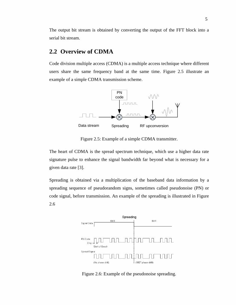
2.2 Overview of CDMA
Code division multiple access (CDMA) is a multiple access technique where different
users share the same frequency band at the same time. Figure 2.5 illustrate an
example of a simple CDMA transmission scheme.
Data stream
PN code
Spreading RF upconversion
Figure 2.5: Example of a simple CDMA transmitter.
The heart of CDMA is the spread spectrum technique, which use a higher data rate
signature pulse to enhance the signal bandwidth far beyond what is necessary for a
given data rate [3].
Spreading is obtained via a multiplication of the baseband data information by a
spreading sequence of pseudorandom signs, sometimes called pseudonoise (PN) or
code signal, before transmission. An example of the spreading is illustrated in Figure
2.6
Figure 2.6: Example of the pseudonoise spreading.
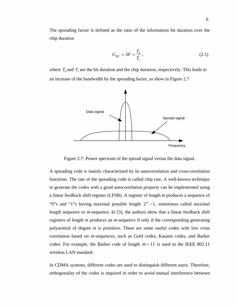
6 The spreading factor is defined as the ratio of the information bit duration over the
chip duration
,c
bMC T
TSFG == (2.1)
where T and T are the bit duration and the chip duration, respectively. This leads to
an increase of the bandwidth by the spreading factor, as show in Figure 2.7
b c
Frequency
Spread signal
Data signal
Figure 2.7: Power spectrum of the spread signal versus the data signal.
A spreading code is mainly characterized by its autocorrelation and cross-correlation
functions. The rate of the spreading code is called chip rate. A well-known technique
to generate the codes with a good autocorrelation property can be implemented using
a linear feedback shift register (LFSR). A register of length m produces a sequence of
“0”s and “1”s having maximal possible length 12 −m , sometimes called maximal
length sequence or m-sequence. In [3], the authors show that a linear feedback shift
registers of length m produces an m-sequence if only if the corresponding generating
polynomial of degree m is primitive. There are some useful codes with low cross
correlation based on m-sequences, such as Gold codes, Kasami codes, and Barker
codes. For example, the Barker code of length 11=m is used in the IEEE 802.11
wireless LAN standard.
In CDMA systems, different codes are used to distinguish different users. Therefore,
orthogonality of the codes is required in order to avoid mutual interference between
7
]the users. Walsh functions [3] have an important role in CDMA signaling. The Walsh
functions , are functions defined on a time interval that is
piecewise constant on time sub-intervals (called chips) of duration . The sign of
the function on the time sub-interval
[ STt 0∈( )tgk Mk ,...,1=
CT
( )Mi ,...,1=thi is given by the component
of the column vector in the Walsh–Hadamard matrix . The
thi
MHikh thk MM ×
Walsh–Hadamard matrices , where M is a power of two, are defined by MH 11 =H
and the recursive relation
⎥⎥
⎦
⎤
⎢⎢
⎣
⎡
−=22
22
MM
MM
M HHHH
H . (2.2)
Walsh function may also be used for orthogonal signaling, sometimes called Walsh
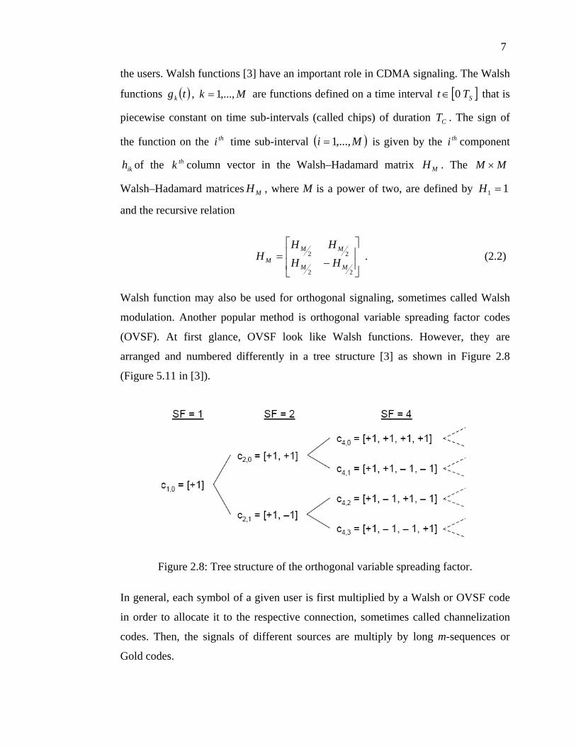
modulation. Another popular method is orthogonal variable spreading factor codes
(OVSF). At first glance, OVSF look like Walsh functions. However, they are
arranged and numbered differently in a tree structure [3] as shown in Figure 2.8
(Figure 5.11 in [3]).
Figure 2.8: Tree structure of the orthogonal variable spreading factor.
In general, each symbol of a given user is first multiplied by a Walsh or OVSF code
in order to allocate it to the respective connection, sometimes called channelization
codes. Then, the signals of different sources are multiply by long m-sequences or
Gold codes.

8 2.3 Fundamentals of MC-CDMA
MC-CDMA, a novel digital modulation and multiple access scheme [1, 2], is a
combination of OFDM and CDMA. Such a combination has the benefits of both
OFDM and CDMA [3]. In MC-CDMA, symbols are modulated on many subcarriers
to introduce frequency diversity instead of using only one carrier like in CDMA.
Thus, MC-CDMA is robust against deep frequency selective fading compared to DS-
CDMA [5]. Each user data is first spread using a given high rate spreading code in
the frequency domain [1]. A fraction of the symbol corresponding to a chip of the
spreading code is transmitted through a different subcarrier [1].
2.3.1 MC-CDMA transmitter model The MC-CDMA transmitter configuration for the user is shown in Figure 2.9. thj
jC1 ( )tf12cos π
jC2 ( )tf22cos π
jGMC
C ( )tfMCGπ2cos
ja
ja
( )tS jMC
( )tf02cos π
jC
1j
C3j
C2
jGM
CC
Figure 2.9: MC-CDMA transmitter.
In this figure, the main difference is that the MC-CDMA scheme transmits the same
symbol in parallel through several subcarriers whereas the OFDM scheme transmits
different symbols. is the spreading code of the user in
the frequency domain, denotes the processing gain, sometimes called the
( ) ⎥⎦⎤
⎢⎣⎡= j
Gjj
j MCCCCtC L21
thj
MCG
9 spreading factor. The input data stream is multiplied by the spreading code with
length . Each chip of the code modulates one subcarrier. The number of
subcarriers is
MCG
MCN G= . The users are separated by different codes. All data
corresponding to the total number of subcarriers are modulated in baseband by an
inverse fast Fourier transform (IFFT) and converted back into serial data. Then, a
cyclic prefix is inserted between the symbols to combat the inter-symbol interference
(ISI) and the inter-carrier interference (ICI) caused by multipath fading. Finally, the
signal is digital to analog converted and upconverted for transmission.
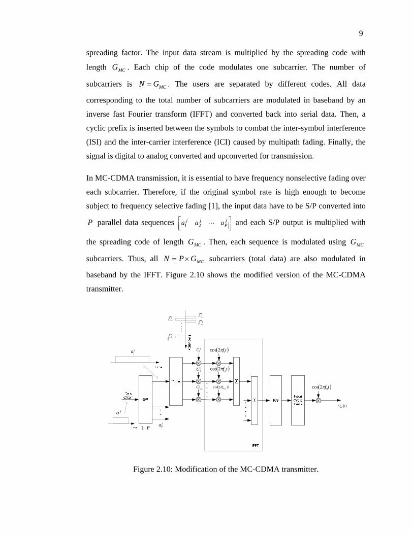
In MC-CDMA transmission, it is essential to have frequency nonselective fading over
each subcarrier. Therefore, if the original symbol rate is high enough to become
subject to frequency selective fading [1], the input data have to be S/P converted into
P parallel data sequences and each S/P output is multiplied with
the spreading code of length . Then, each sequence is modulated using
subcarriers. Thus, all
⎥⎦⎤
⎢⎣⎡ j
Pjj aaa L21
MCG MCG
MCGPN ×= subcarriers (total data) are also modulated in
baseband by the IFFT. Figure 2.10 shows the modified version of the MC-CDMA
transmitter.
jC1 ( )tf12cos π
jC2 ( )tf22cos π
jGMC
C ( )tfMCGπ2cos
ja1
ja( )tS j
MC
( )tf02cos π
jPaP:1
jC
1j
C3
jC
2jGM
CC
Figure 2.10: Modification of the MC-CDMA transmitter.
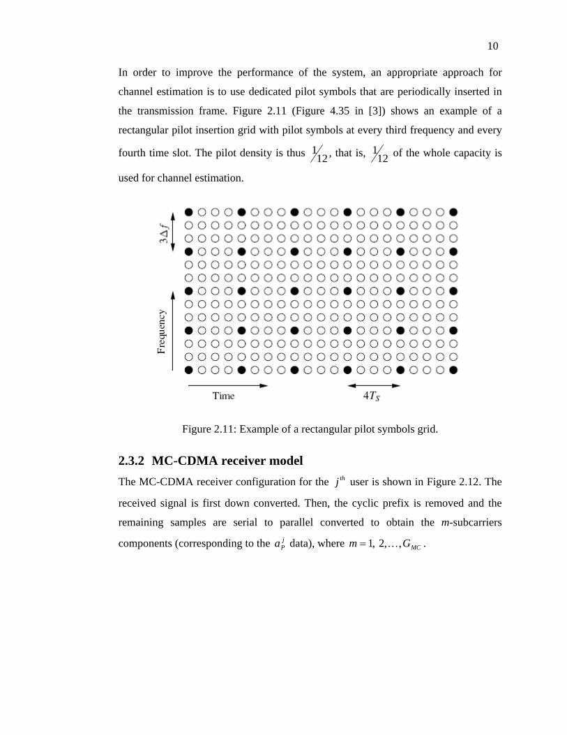
10 In order to improve the performance of the system, an appropriate approach for
channel estimation is to use dedicated pilot symbols that are periodically inserted in
the transmission frame. Figure 2.11 (Figure 4.35 in [3]) shows an example of a
rectangular pilot insertion grid with pilot symbols at every third frequency and every
fourth time slot. The pilot density is thus 121
121, that is, of the whole capacity is
used for channel estimation.
Figure 2.11: Example of a rectangular pilot symbols grid.
2.3.2 MC-CDMA receiver model The MC-CDMA receiver configuration for the user is shown in Figure 2.12. The
received signal is first down converted. Then, the cyclic prefix is removed and the
remaining samples are serial to parallel converted to obtain the m-subcarriers
components (corresponding to the data), where
thj
jPa MCGm ,,2,1 K= .
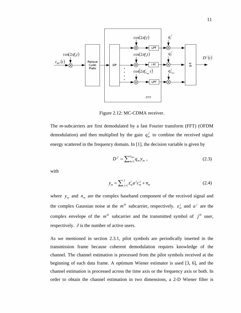
11
( )tf02cos π
( )trMC
( )tf12cos π
( )tf22cos π
( )tfMCGπ2cos
'1jq
'2jq
'jGMC
q
( )tD j '
Figure 2.12: MC-CDMA receiver.
The m-subcarriers are first demodulated by a fast Fourier transform (FFT) (OFDM
demodulation) and then multiplied by the gain to combine the received signal
energy scattered in the frequency domain. In [1], the decision variable is given by
'jmq
,1
' ∑ == MCG
m mmj yqD (2.3)
with
1
J i j jm m mj my z a c n
== +∑ (2.4)
where and are the complex baseband component of the received signal and
the complex Gaussian noise at the subcarrier, respectively. and are the
complex envelope of the subcarrier and the transmitted symbol of user,
respectively. is the number of active users.
my mn
jmzthm ja
thjthm
J
As we mentioned in section 2.3.1, pilot symbols are periodically inserted in the
transmission frame because coherent demodulation requires knowledge of the
channel. The channel estimation is processed from the pilot symbols received at the
beginning of each data frame. A optimum Wiener estimator is used [3, 6], and the
channel estimation is processed across the time axis or the frequency axis or both. In
order to obtain the channel estimation in two dimensions, a 2-D Wiener filter is
12 derived and analyzed given an arbitrary sampling grid, an arbitrary selection of
observations, and the possibility of a model mismatch [6]. Fortunately, the 2-D
Wiener filter is simply implemented by using two cascaded orthogonal 1-D filters and
shown to be virtually as good as a true 2-D filter. That is, the 1-D channel estimation
is first performed, for example, along the frequency axis at the time slots where the
pilots are located. At these time slots, there is a channel estimate available for every
frequency. Then, the 1-D channel estimation along the time axis can be performed
and an estimate for all time-frequency positions is available.
Other important aspects of the MC-CDMA receiver such as timing synchronization,
frequency synchronization, frame synchronization, frequency offset estimation,
interference cancellation, timing recovery, channel coding, and channel equalization
will be reviewed in the following sections dealing with implementation.
3. OFDM implementation
3.1 Modulation and demodulation
In OFDM modulation, the input serial data stream is serial to parallel converted into
the symbol size required for transmission, e.g. 1 bit/symbol, 2 bits/symbol, 4
bits/symbol for BPSK, QPSK, 16-QAM, respectively. The data on each symbol is
mapped to a suitable phase and amplitude based on the given modulation method. In
[7], a new efficient implementation for OFDM, offset QAM, is proposed. This
method uses nearly half the number of the computations required for each symbol
period by exploiting the symmetries in the transmitted sequences [7]. The parallel
mapped data is modulated by using the inverse fast Fourier transform. A number of
IFFT architectures have been introduced to reduce the power consumption, or the
complexity.
In [8], a novel 64-point FFT low power pipelined radix-4 architecture is presented
for MC-CDMA receivers. The use of coefficient ordering and clock gating is
employed, thus providing a power reduction for the receiver.
Fortunately, there are some high performance commercial FFT/IFFT cores provided
by companies such as Xilinx, Altera, or Actel. The FFT/IFFT core provides several
architecture options to offer a trade-off between core size and transform time. Thus,
the use of the FFT/IFFT core is very efficient for the implementation of MC-CDMA
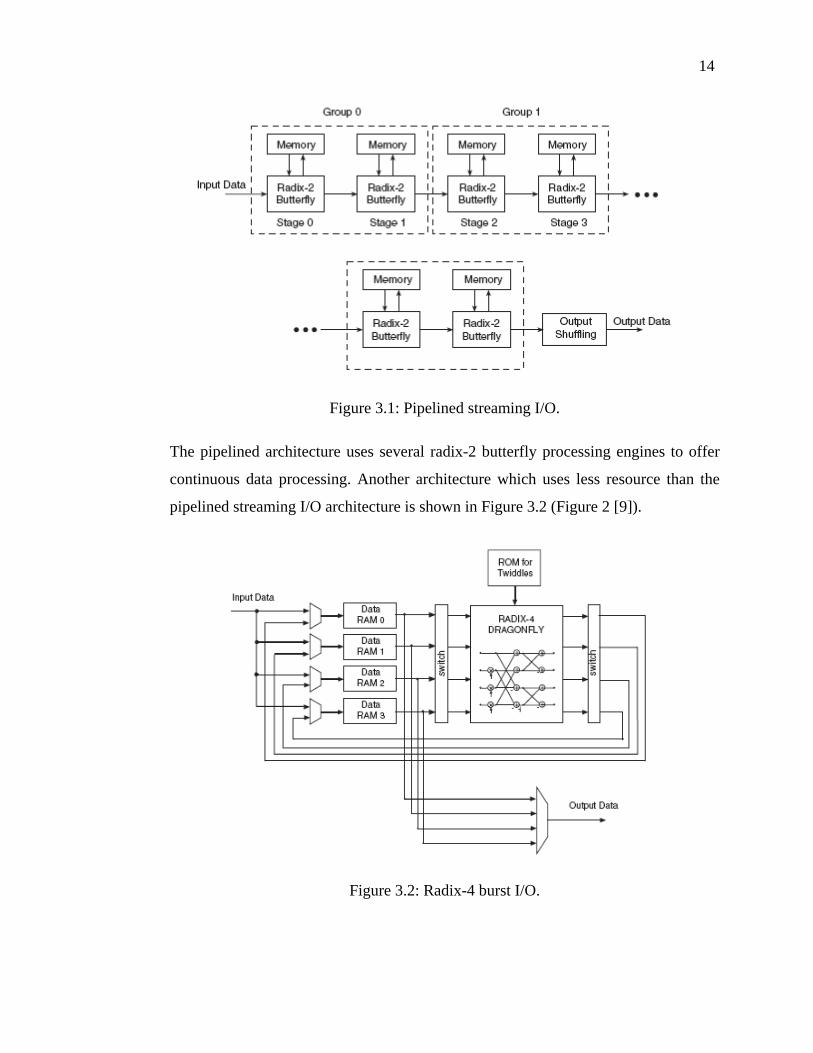
systems. Figure 3.1 (Figure 1 in [9]) illustrates the pipelined streaming I/O
architecture which is provided by Xilinx.
14
Figure 3.1: Pipelined streaming I/O.
The pipelined architecture uses several radix-2 butterfly processing engines to offer
continuous data processing. Another architecture which uses less resource than the
pipelined streaming I/O architecture is shown in Figure 3.2 (Figure 2 [9]).
Figure 3.2: Radix-4 burst I/O.
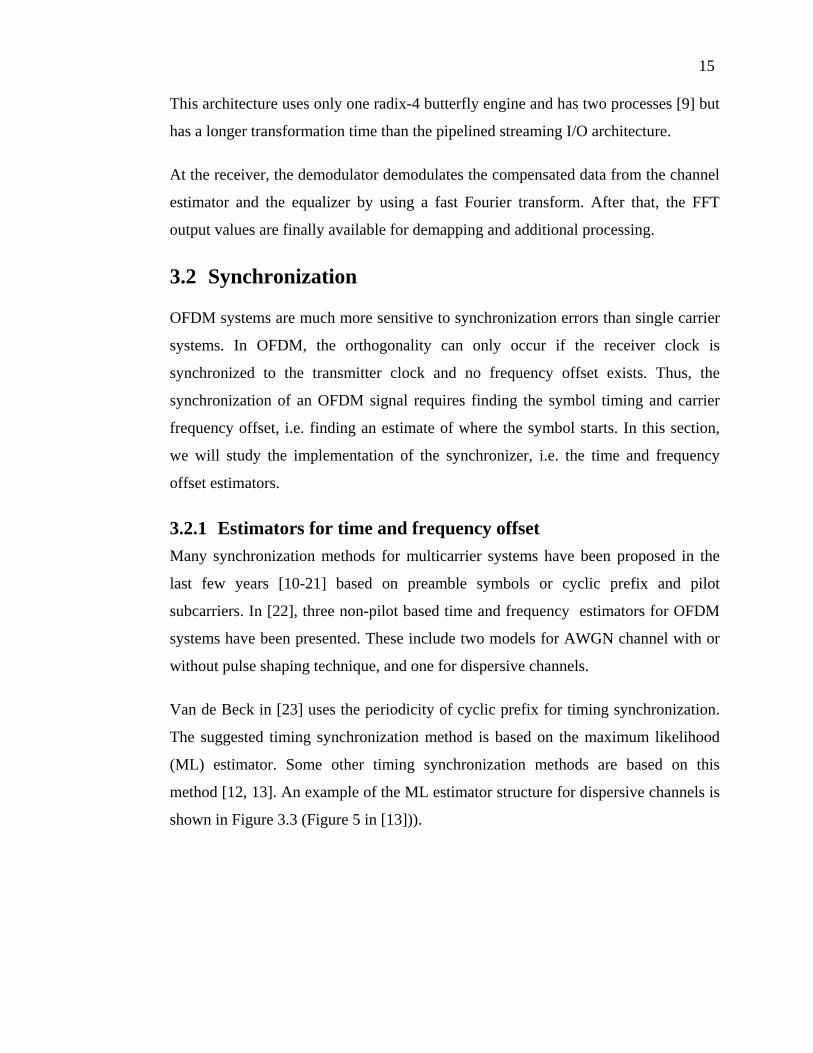
15 This architecture uses only one radix-4 butterfly engine and has two processes [9] but
has a longer transformation time than the pipelined streaming I/O architecture.
At the receiver, the demodulator demodulates the compensated data from the channel
estimator and the equalizer by using a fast Fourier transform. After that, the FFT
output values are finally available for demapping and additional processing.
3.2 Synchronization
OFDM systems are much more sensitive to synchronization errors than single carrier
systems. In OFDM, the orthogonality can only occur if the receiver clock is
synchronized to the transmitter clock and no frequency offset exists. Thus, the
synchronization of an OFDM signal requires finding the symbol timing and carrier
frequency offset, i.e. finding an estimate of where the symbol starts. In this section,
we will study the implementation of the synchronizer, i.e. the time and frequency
offset estimators.
3.2.1 Estimators for time and frequency offset Many synchronization methods for multicarrier systems have been proposed in the
last few years [10-21] based on preamble symbols or cyclic prefix and pilot
subcarriers. In [22], three non-pilot based time and frequency estimators for OFDM
systems have been presented. These include two models for AWGN channel with or
without pulse shaping technique, and one for dispersive channels.
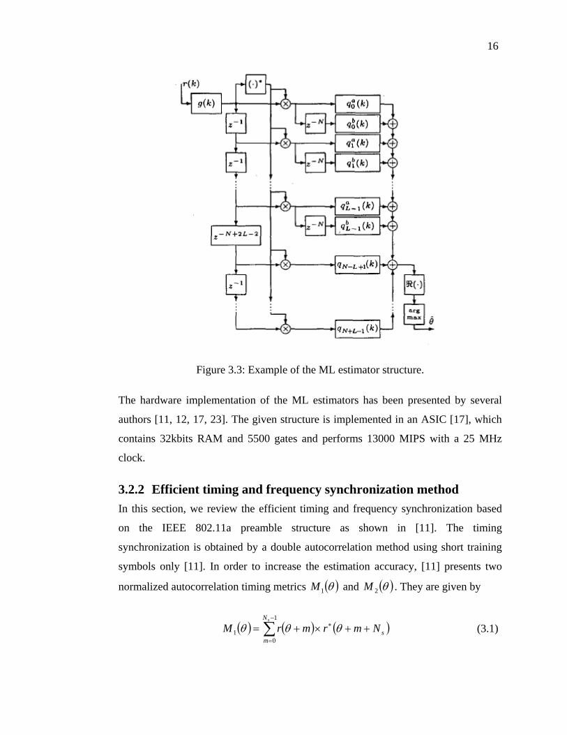
Van de Beck in [23] uses the periodicity of cyclic prefix for timing synchronization.
The suggested timing synchronization method is based on the maximum likelihood
(ML) estimator. Some other timing synchronization methods are based on this
method [12, 13]. An example of the ML estimator structure for dispersive channels is
shown in Figure 3.3 (Figure 5 in [13])).
16
Figure 3.3: Example of the ML estimator structure.
The hardware implementation of the ML estimators has been presented by several
authors [11, 12, 17, 23]. The given structure is implemented in an ASIC [17], which
contains 32kbits RAM and 5500 gates and performs 13000 MIPS with a 25 MHz
clock.
3.2.2 Efficient timing and frequency synchronization method In this section, we review the efficient timing and frequency synchronization based
on the IEEE 802.11a preamble structure as shown in [11]. The timing
synchronization is obtained by a double autocorrelation method using short training
symbols only [11]. In order to increase the estimation accuracy, [11] presents two
normalized autocorrelation timing metrics ( )θ1M ( )θ2M and . They are given by
(3.1) ( ) ( ) ( )∑−
=
∗ ++×+=1
01
sN
msNmrmrM θθθ

17 and
(3.2) ( ) ( ) ( )∑−
=
∗ ++×+=1
02 2
sN
msNmrmrM θθθ
where is the delay of one short symbol. We can see that the second metric 16=sN
( )θ2M is defined as the correlation between the received signal and itself with a
delay of two short symbols . The triangular shaped timing metric is obtained by
subtracting
sN2
( )θ2M ( )θ1M ( ) ( )θθ 21 MM − from . The peak value of the difference
indicates the start of the 9th short symbol. That is, the timing estimate is given by
( ) ( )( θθθθ 21maxarg MM −=
∧ ) (3.3)
Figure 3.4 (Figure 2 in [16]) shows an example of the timing metric for double
autocorrelation
Figure 3.4: Timing metric for double autocorrelation.
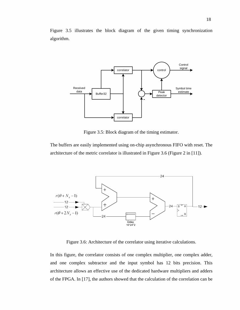
18 Figure 3.5 illustrates the block diagram of the given timing synchronization
algorithm.
Buffer32
correlator
correlator
Peak detector
control
-
Received data
Control signal
Symbol time estimate
Figure 3.5: Block diagram of the timing estimator.
The buffers are easily implemented using on-chip asynchronous FIFO with reset. The
architecture of the metric correlator is illustrated in Figure 3.6 (Figure 2 in [11]).
Figure 3.6: Architecture of the correlator using iterative calculations.
In this figure, the correlator consists of one complex multiplier, one complex adder,
and one complex subtractor and the input symbol has 12 bits precision. This
architecture allows an effective use of the dedicated hardware multipliers and adders
of the FPGA. In [17], the authors showed that the calculation of the correlation can be
19 done with fewer bits. In a hardware implementation, choosing the correct word length
will improve the performance of the design. Thus, the use of four bits from every
input symbol is enough to calculate the correlation with 12 bits accuracy. The peak
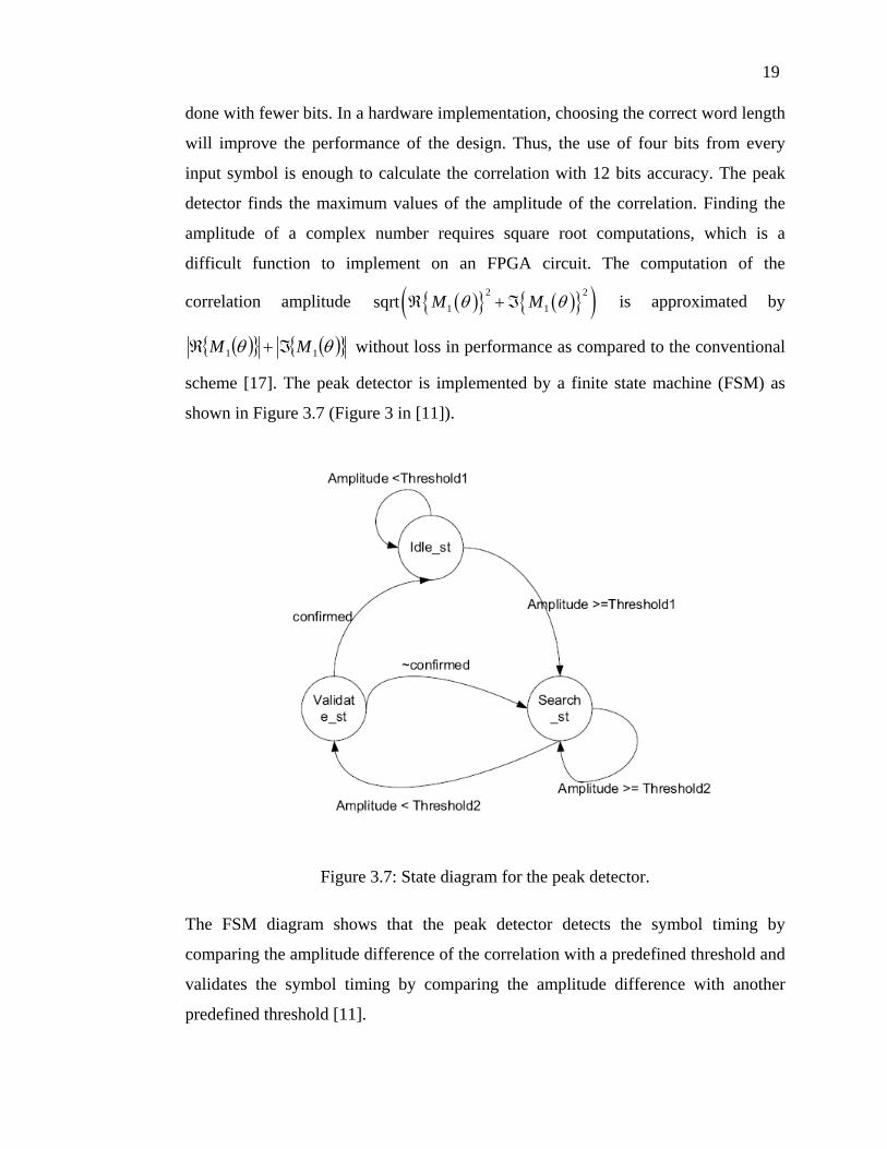
detector finds the maximum values of the amplitude of the correlation. Finding the
amplitude of a complex number requires square root computations, which is a
difficult function to implement on an FPGA circuit. The computation of the
correlation amplitude ( ){ } ( ){ }( )21 1sqrt M Mθℜ + ℑ
2θ is approximated by
( ){ } ( ){ }θθ 11 MM ℑ+ℜ without loss in performance as compared to the conventional
scheme [17]. The peak detector is implemented by a finite state machine (FSM) as
shown in Figure 3.7 (Figure 3 in [11]).
Figure 3.7: State diagram for the peak detector.
The FSM diagram shows that the peak detector detects the symbol timing by
comparing the amplitude difference of the correlation with a predefined threshold and
validates the symbol timing by comparing the amplitude difference with another
predefined threshold [11].
20 At the receiver side, the main difference between two consecutive short training
symbol is the phase difference caused by carrier frequency offset [11]. Thus, the
coarse frequency estimation using the ( )θ1M can be expressed as
1angle M θε
π
∧
∧
⎛ ⎞⎛ ⎞⎜ ⎟⎜ ⎟⎝ ⎠⎝ ⎠= (3.4)
where and are frequency estimate and symbol timing estimate, respectively. In
order to improve the accuracy of the frequency estimation, the autocorrelation over
four short training symbols must be performed [11]. The averaging autocorrelation is
given by
∧
ε∧
θ
(3.5) ( ) ( ) ( )∑−
=
∗ ++×+=14
0
sN
msNmrmrM θθθ
and the frequency estimate is
angle.f
M θε
π
∧
∧
⎛ ⎞⎛ ⎞⎜ ⎟⎜ ⎟⎝ ⎠⎝ ⎠= (3.6)
Finally, the frequency offset compensation is given by
( ) ( ) Nnf
enrnr
∧
−×=
επ2' (3.7)
where and are the received sample and the frequency offset compensated
sample, respectively. Figure 3.8 (Figure 1 in [11]) illustrates the block diagram of the
given frequency synchronization algorithm.
( )nr ( )nr '
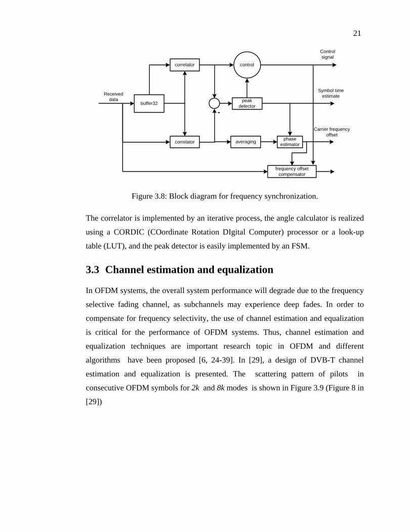
21
buffer32
correlator
correlator
peak detector
control
-
Received data
signal
Symbol time estimate
Control
averaging phase estimator
frequency offset compensator
Carrier frequency offset
Figure 3.8: Block diagram for frequency synchronization.
The correlator is implemented by an iterative process, the angle calculator is realized
using a CORDIC (COordinate Rotation DIgital Computer) processor or a look-up
table (LUT), and the peak detector is easily implemented by an FSM.
3.3 Channel estimation and equalization
In OFDM systems, the overall system performance will degrade due to the frequency
selective fading channel, as subchannels may experience deep fades. In order to
compensate for frequency selectivity, the use of channel estimation and equalization
is critical for the performance of OFDM systems. Thus, channel estimation and
equalization techniques are important research topic in OFDM and different
algorithms have been proposed [6, 24-39]. In [29], a design of DVB-T channel
estimation and equalization is presented. The scattering pattern of pilots in
consecutive OFDM symbols for 2k and 8k modes is shown in Figure 3.9 (Figure 8 in
[29])
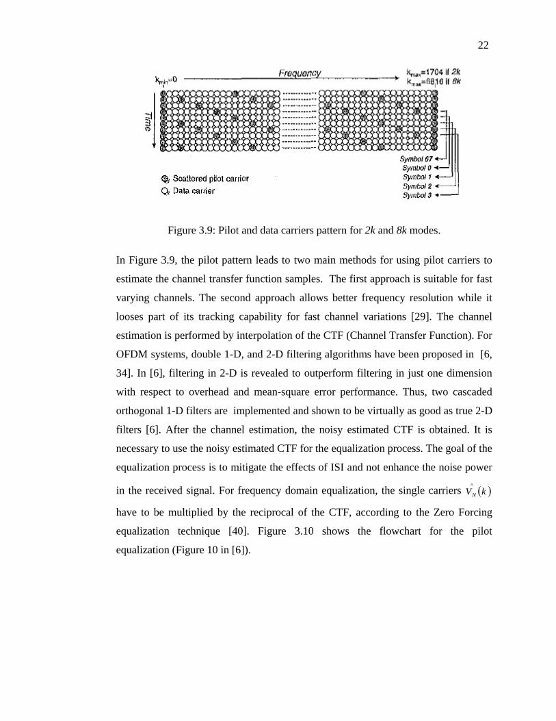
22
Figure 3.9: Pilot and data carriers pattern for 2k and 8k modes.
In Figure 3.9, the pilot pattern leads to two main methods for using pilot carriers to
estimate the channel transfer function samples. The first approach is suitable for fast
varying channels. The second approach allows better frequency resolution while it
looses part of its tracking capability for fast channel variations [29]. The channel
estimation is performed by interpolation of the CTF (Channel Transfer Function). For
OFDM systems, double 1-D, and 2-D filtering algorithms have been proposed in [6,
34]. In [6], filtering in 2-D is revealed to outperform filtering in just one dimension
with respect to overhead and mean-square error performance. Thus, two cascaded
orthogonal 1-D filters are implemented and shown to be virtually as good as true 2-D
filters [6]. After the channel estimation, the noisy estimated CTF is obtained. It is
necessary to use the noisy estimated CTF for the equalization process. The goal of the
equalization process is to mitigate the effects of ISI and not enhance the noise power
in the received signal. For frequency domain equalization, the single carriers
have to be multiplied by the reciprocal of the CTF, according to the Zero Forcing
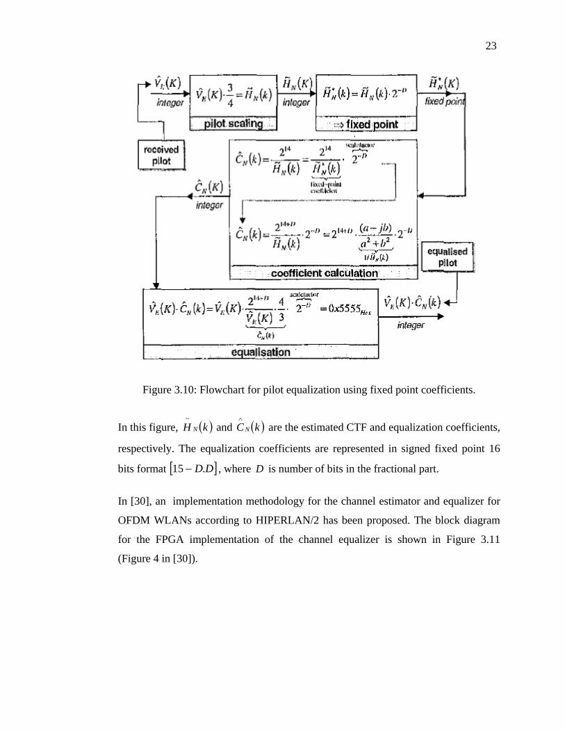
equalization technique [40]. Figure 3.10 shows the flowchart for the pilot
equalization (Figure 10 in [6]).
( )kVN
∧
23
Figure 3.10: Flowchart for pilot equalization using fixed point coefficients.
In this figure, and are the estimated CTF and equalization coefficients,
respectively. The equalization coefficients are represented in signed fixed point 16
bits format
( )kH N
~( )kC N
∧
[ ]DD.15 − , where is number of bits in the fractional part. D
In [30], an implementation methodology for the channel estimator and equalizer for
OFDM WLANs according to HIPERLAN/2 has been proposed. The block diagram
for the FPGA implementation of the channel equalizer is shown in Figure 3.11
(Figure 4 in [30]).
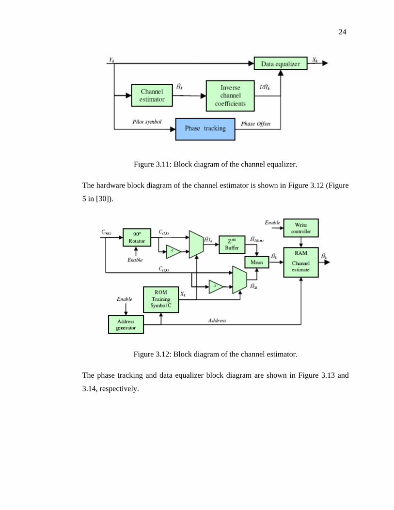
24
Figure 3.11: Block diagram of the channel equalizer.
The hardware block diagram of the channel estimator is shown in Figure 3.12 (Figure
5 in [30]).
Figure 3.12: Block diagram of the channel estimator.
The phase tracking and data equalizer block diagram are shown in Figure 3.13 and
3.14, respectively.

25
Figure 3.13: Block diagram for phase tracking.
Figure 3.14: Block diagram of the data equalizer.
The data equalizer corrects the distortion phase and the attenuation of the received
signal using the inverse of the estimated channel coefficients. The inverse of the
estimated channel coefficients can be obtained by the CORDIC or Hung algorithms
[30]. The Hung algorithm is a high radix division algorithm based on a Taylor series
expansion. It combines the first two terms of the Taylor series, and requires only a
small look-up table to generate accurate results [41].
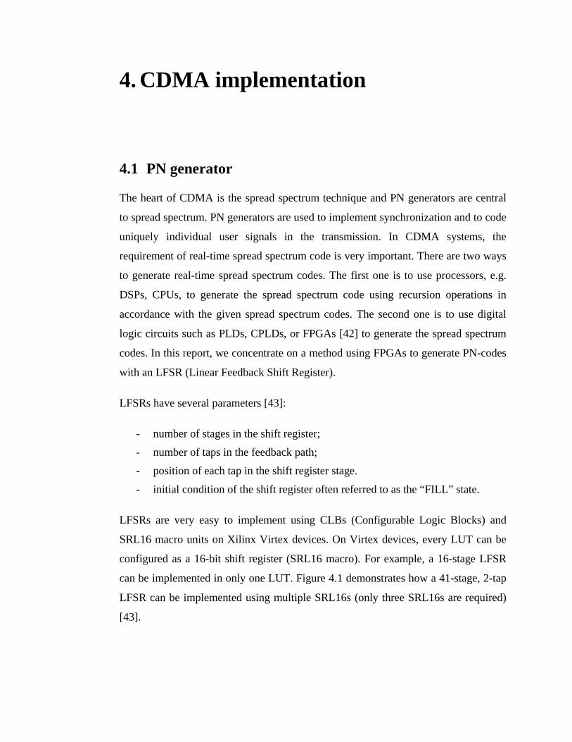
4. CDMA implementation
4.1 PN generator
The heart of CDMA is the spread spectrum technique and PN generators are central
to spread spectrum. PN generators are used to implement synchronization and to code
uniquely individual user signals in the transmission. In CDMA systems, the
requirement of real-time spread spectrum code is very important. There are two ways
to generate real-time spread spectrum codes. The first one is to use processors, e.g.
DSPs, CPUs, to generate the spread spectrum code using recursion operations in
accordance with the given spread spectrum codes. The second one is to use digital
logic circuits such as PLDs, CPLDs, or FPGAs [42] to generate the spread spectrum
codes. In this report, we concentrate on a method using FPGAs to generate PN-codes
with an LFSR (Linear Feedback Shift Register).
LFSRs have several parameters [43]:
- number of stages in the shift register;
- number of taps in the feedback path;
- position of each tap in the shift register stage.
- initial condition of the shift register often referred to as the “FILL” state.
LFSRs are very easy to implement using CLBs (Configurable Logic Blocks) and
SRL16 macro units on Xilinx Virtex devices. On Virtex devices, every LUT can be
configured as a 16-bit shift register (SRL16 macro). For example, a 16-stage LFSR
can be implemented in only one LUT. Figure 4.1 demonstrates how a 41-stage, 2-tap
LFSR can be implemented using multiple SRL16s (only three SRL16s are required)
[43].

27
Figure 4.1: 41-stage, 2-tap LFSR with three SRL16s.
In CDMA, the overall FPGA utilization can be reduced considerably by taking
advantage of SRLs.
4.2 Matched filter
In CDMA systems, the operation of matched filtering is the same as correlating the
input signal with a copy of itself. The matched filter indicates when a code sequence
is detected in the input data stream. The output of a matched filter will be the score
value. The peak of the score value indicates a good correlation with the code
sequence of interest. Figure 4.2 illustrates the basic operation of a matched filter
(Figure 1 in [44]).
Figure 4.2: CDMA matched filter basic operation.
The input data stream is slid past the desired code sequence until the highest score
value is obtained. For example, with a code sequence of 16 chips, a perfect match is
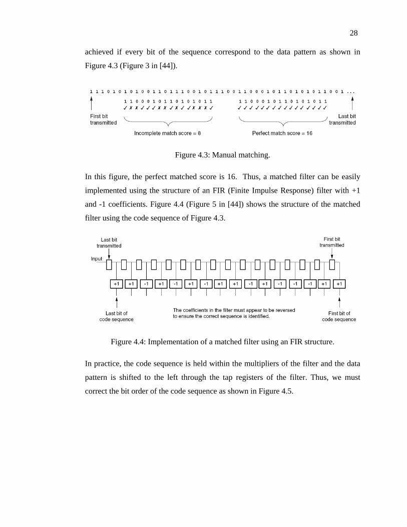
28 achieved if every bit of the sequence correspond to the data pattern as shown in
Figure 4.3 (Figure 3 in [44]).
Figure 4.3: Manual matching.
In this figure, the perfect matched score is 16. Thus, a matched filter can be easily
implemented using the structure of an FIR (Finite Impulse Response) filter with +1
and -1 coefficients. Figure 4.4 (Figure 5 in [44]) shows the structure of the matched
filter using the code sequence of Figure 4.3.
Figure 4.4: Implementation of a matched filter using an FIR structure.
In practice, the code sequence is held within the multipliers of the filter and the data
pattern is shifted to the left through the tap registers of the filter. Thus, we must
correct the bit order of the code sequence as shown in Figure 4.5.
29
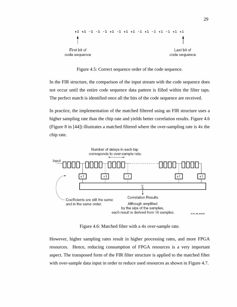
Figure 4.5: Correct sequence order of the code sequence.
In the FIR structure, the comparison of the input stream with the code sequence does
not occur until the entire code sequence data pattern is filled within the filter taps.
The perfect match is identified once all the bits of the code sequence are received.
In practice, the implementation of the matched filtered using an FIR structure uses a
higher sampling rate than the chip rate and yields better correlation results. Figure 4.6
(Figure 8 in [44]) illustrates a matched filtered where the over-sampling rate is 4x the
chip rate.
Figure 4.6: Matched filter with a 4x over-sample rate.
However, higher sampling rates result in higher processing rates, and more FPGA
resources. Hence, reducing consumption of FPGA resources is a very important
aspect. The transposed form of the FIR filter structure is applied to the matched filter
with over-sample data input in order to reduce used resources as shown in Figure 4.7.
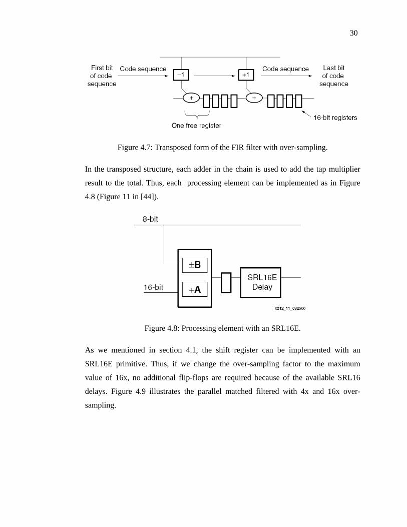
30
Figure 4.7: Transposed form of the FIR filter with over-sampling.
In the transposed structure, each adder in the chain is used to add the tap multiplier
result to the total. Thus, each processing element can be implemented as in Figure
4.8 (Figure 11 in [44]).
Figure 4.8: Processing element with an SRL16E.
As we mentioned in section 4.1, the shift register can be implemented with an
SRL16E primitive. Thus, if we change the over-sampling factor to the maximum
value of 16x, no additional flip-flops are required because of the available SRL16
delays. Figure 4.9 illustrates the parallel matched filtered with 4x and 16x over-
sampling.
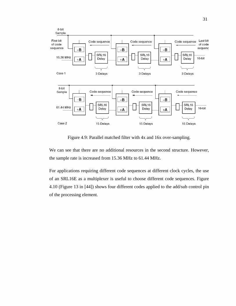
31
Figure 4.9: Parallel matched filter with 4x and 16x over-sampling.
We can see that there are no additional resources in the second structure. However,
the sample rate is increased from 15.36 MHz to 61.44 MHz.
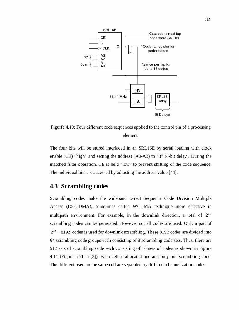
For applications requiring different code sequences at different clock cycles, the use
of an SRL16E as a multiplexer is useful to choose different code sequences. Figure
4.10 (Figure 13 in [44]) shows four different codes applied to the add/sub control pin
of the processing element.
32
Figurfe 4.10: Four different code sequences applied to the control pin of a processing
element.
The four bits will be stored interlaced in an SRL16E by serial loading with clock
enable (CE) “high” and setting the address (A0-A3) to “3” (4-bit delay). During the
matched filter operation, CE is held “low” to prevent shifting of the code sequence.
The individual bits are accessed by adjusting the address value [44].
4.3 Scrambling codes
Scrambling codes make the wideband Direct Sequence Code Division Multiple
Access (DS-CDMA), sometimes called WCDMA technique more effective in
multipath environment. For example, in the downlink direction, a total of
scrambling codes can be generated. However not all codes are used. Only a part of
codes is used for downlink scrambling. These 8192 codes are divided into
64 scrambling code groups each consisting of 8 scrambling code sets. Thus, there are
512 sets of scrambling code each consisting of 16 sets of codes as shown in Figure
4.11 (Figure 5.51 in [3]). Each cell is allocated one and only one scrambling code.
The different users in the same cell are separated by different channelization codes.
182
8192213 =
33
Figure 4.11: Division of scrambling sequences into different groups and sets.
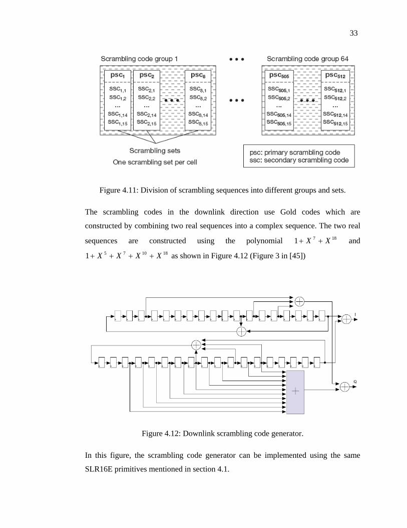
The scrambling codes in the downlink direction use Gold codes which are
constructed by combining two real sequences into a complex sequence. The two real
sequences are constructed using the polynomial 1871 XX ++ and 1810751 XXXX ++++ as shown in Figure 4.12 (Figure 3 in [45])
Figure 4.12: Downlink scrambling code generator.
In this figure, the scrambling code generator can be implemented using the same
SLR16E primitives mentioned in section 4.1.
34 4.4 Channelization codes
Transmissions from a single user are separated by channelization codes, i.e.,
download connections within one sector and the dedicated physical channel on the
uplink [45]. The channelization codes used both uplink and downlink and OVSF
codes preserve the orthogonality between the downlink channels of different rates
and spreading codes. As we mentioned in section 2.2, the OVSF codes are recursively
generated. Thus, the OVSF codes can be implemented using software in a PowerPC
embedded processor in a Virtex device, on a special-purpose processor or in a
combinational logic circuit [46]. Furthermore, OVSF codes can be obtained using a
look-up table or embedded block RAM within FPGA which stores the code
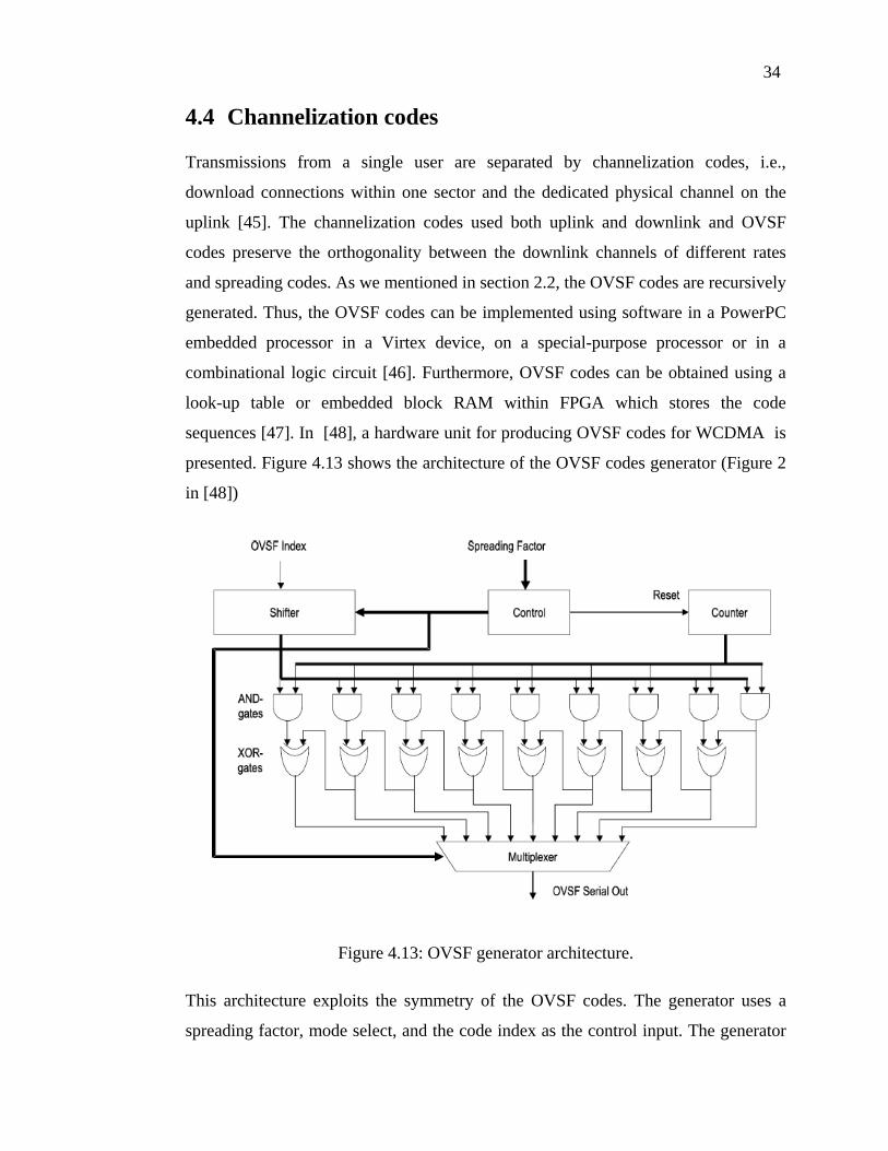
sequences [47]. In [48], a hardware unit for producing OVSF codes for WCDMA is
presented. Figure 4.13 shows the architecture of the OVSF codes generator (Figure 2
in [48])
Figure 4.13: OVSF generator architecture.
This architecture exploits the symmetry of the OVSF codes. The generator uses a
spreading factor, mode select, and the code index as the control input. The generator
35 consists of five blocks: control, shifter, counter, generator-array and multiplexer [48].
The control block receives the spreading factor and converts it into 3-bit control
signal for the Shifter block and the Multiplexer for selecting the desired OVSF code.
The shifter block stores the 9-bit (0-511) OVSF-index of the desired code. The index
is shifted left according to the 3-bit control signal set by the control block. The
counter counts up to the desired spreading factor providing the index to the code bits
and each of its 9 output bits is connected to the corresponding AND/XOR gate pair to
be used as a control signal. The generator array produces the actual OVSF code
sequence according to these control signals [48].
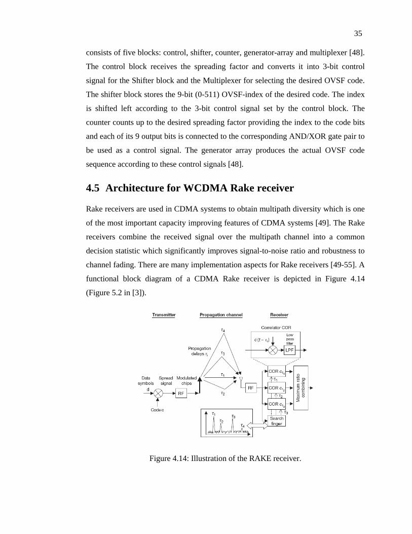
4.5 Architecture for WCDMA Rake receiver
Rake receivers are used in CDMA systems to obtain multipath diversity which is one
of the most important capacity improving features of CDMA systems [49]. The Rake
receivers combine the received signal over the multipath channel into a common
decision statistic which significantly improves signal-to-noise ratio and robustness to
channel fading. There are many implementation aspects for Rake receivers [49-55]. A
functional block diagram of a CDMA Rake receiver is depicted in Figure 4.14
(Figure 5.2 in [3]).
Figure 4.14: Illustration of the RAKE receiver.
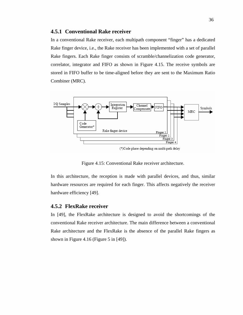
36 4.5.1 Conventional Rake receiver In a conventional Rake receiver, each multipath component “finger” has a dedicated
Rake finger device, i.e., the Rake receiver has been implemented with a set of parallel
Rake fingers. Each Rake finger consists of scramble/channelization code generator,
correlator, integrator and FIFO as shown in Figure 4.15. The receive symbols are
stored in FIFO buffer to be time-aligned before they are sent to the Maximum Ratio
Combiner (MRC).
Figure 4.15: Conventional Rake receiver architecture.
In this architecture, the reception is made with parallel devices, and thus, similar
hardware resources are required for each finger. This affects negatively the receiver
hardware efficiency [49].
4.5.2 FlexRake receiver In [49], the FlexRake architecture is designed to avoid the shortcomings of the
conventional Rake receiver architecture. The main difference between a conventional
Rake architecture and the FlexRake is the absence of the parallel Rake fingers as
shown in Figure 4.16 (Figure 5 in [49]).
37
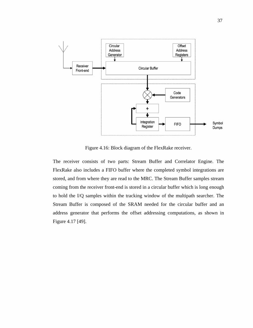
Figure 4.16: Block diagram of the FlexRake receiver.
The receiver consists of two parts: Stream Buffer and Correlator Engine. The
FlexRake also includes a FIFO buffer where the completed symbol integrations are
stored, and from where they are read to the MRC. The Stream Buffer samples stream
coming from the receiver front-end is stored in a circular buffer which is long enough
to hold the I/Q samples within the tracking window of the multipath searcher. The
Stream Buffer is composed of the SRAM needed for the circular buffer and an
address generator that performs the offset addressing computations, as shown in
Figure 4.17 [49].
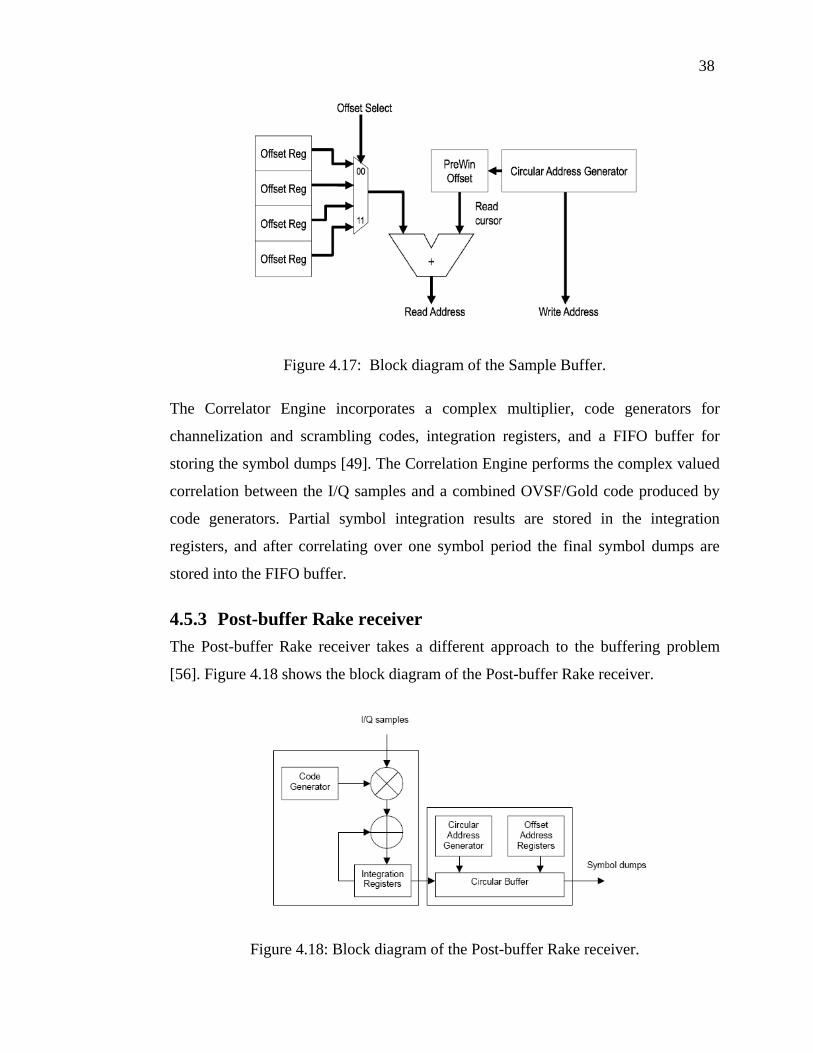
38
Figure 4.17: Block diagram of the Sample Buffer.
The Correlator Engine incorporates a complex multiplier, code generators for
channelization and scrambling codes, integration registers, and a FIFO buffer for
storing the symbol dumps [49]. The Correlation Engine performs the complex valued
correlation between the I/Q samples and a combined OVSF/Gold code produced by
code generators. Partial symbol integration results are stored in the integration
registers, and after correlating over one symbol period the final symbol dumps are
stored into the FIFO buffer.
4.5.3 Post-buffer Rake receiver The Post-buffer Rake receiver takes a different approach to the buffering problem
[56]. Figure 4.18 shows the block diagram of the Post-buffer Rake receiver.
Figure 4.18: Block diagram of the Post-buffer Rake receiver.
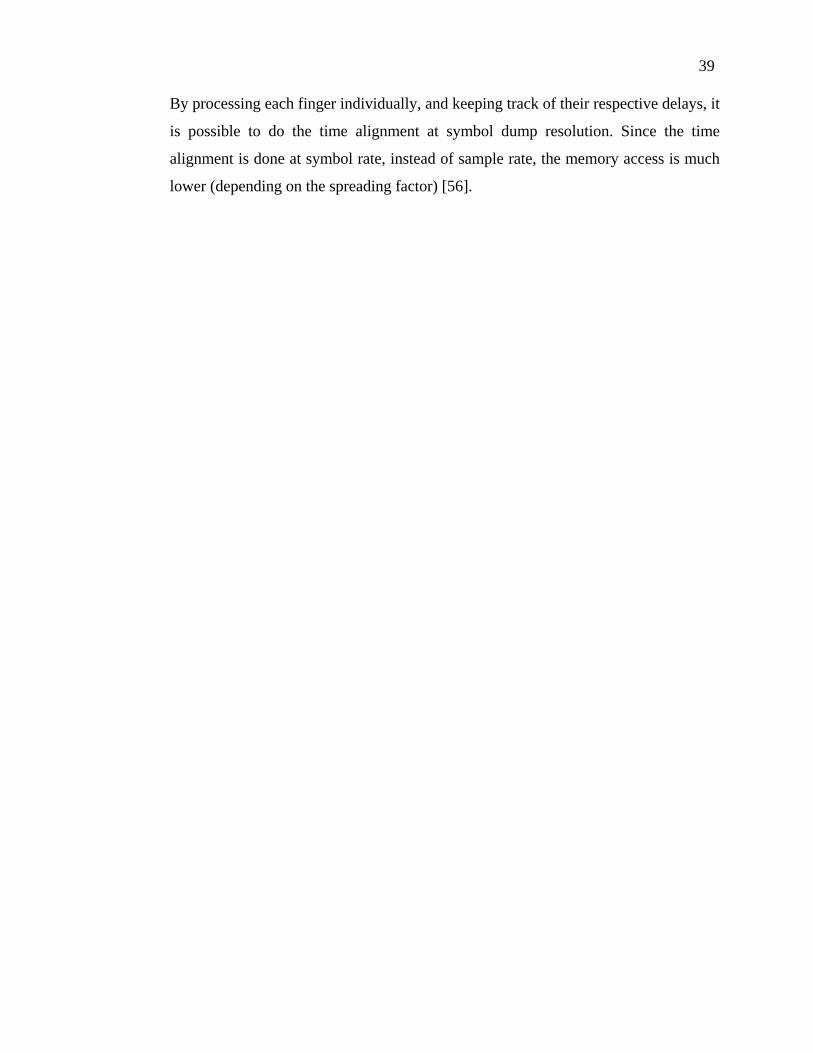
39 By processing each finger individually, and keeping track of their respective delays, it
is possible to do the time alignment at symbol dump resolution. Since the time
alignment is done at symbol rate, instead of sample rate, the memory access is much
lower (depending on the spreading factor) [56].
5. Conclusions
In this report, the fundamentals of MC-CDMA, a novel digital modulation and
multiple access scheme, were studied for 4G cellular mobile radio systems. In order
to prepare for the implementation of MC-CDMA systems, we reviewed the current
state-of-the art trends for implementation of OFDM and CDMA using Field
Programmable Gate Array (FPGA) devices.
FPGA implementation of OFDM and CDMA have been categorized according to
modulation/demodulation, spreading, detection, channel estimation, synchronization,
frequency offset estimation, timing recovery, and equalization. The implementation
uses some primitives of Xilinx FPGAs which are optimized for resource utilization.
References [1] S. Hara and R. Prasad, "Overview of Multicarrier CDMA," IEEE
Communications Magazine, vol. 35, pp. 126-133, 1997.
[2] S. L. Nous, F. Nouvel, and J.-F. Hélard, "Design and Implementation of MC-
CDMA Systems for Future Wireless Networks," EURASIP Journal on
Applied Signal Processing, pp. 1604-1615, 2004.
[3] H. Schulze and C. Luders, Theory and applications of OFDM and CDMA:
Wiley, 2005.
[4] J. Bingham, "Multicarrier modulation for data transmission: an idea whose
time has come," Communications Magazine, IEEE, vol. 28, pp. 5 - 14, 1990.
[5] H. Lui, Signal processing application in CDMA communication: Artech
House Publisher, 2000.
[6] P. Hoecher, S. Kaiser, and P. Roberson, "Two-dimensional Pilot-Symbol-
Aided Channel Estimation by Wienner Filtering," IEEE International
Conference on Acoustics, Speech, and Signal Processing, vol. 3, pp. 1845 -
1848, 1997.
[7] L. Vangelista and N. Laurenti, "Efficient implementations and alternative
architectures for OFDM-OQAM systems," IEEE Transactions on
Communications, vol. 49, pp. 664 - 675, 2001.
[8] M. Hasan, T. Arslan, and J. Thompson, "A Novel Low Power Pipelined
Architecture for a MC-CDMA receiver," 3rd International Symposium on
Image and Signal Processing and Analysis, vol. 2, pp. 18-20, 2003.
[9] Xilinx, Fast Fourier Transform v2.0, vol. LogicCore: Xilinx, 2003.
[10] S. Johansson, P. Nilsson, and M. Torkelson, "Implementation of an OFDM
synchronization algorithm," 42nd Midwest Symposium on Circuits and
Systems, vol. 1, pp. 228-231, 1999.
[11] K. Wang, J. Singh, and M. Faulkner, "FPGA Implementation of an OFDM-
WLAN Synchronizer," Second IEEE International Workshop on Electronic
Design, Test and Applications, pp. 89 - 94, 2004.
42 [12] Y.-T. Hwang, K.-W. Liao, and C.-H. Wu, "FPGA realization of an OFDM
frame synchronization design for dispersive channels," International
Symposium on Circuits and Systems, vol. 2, pp. 256-259, 2003.
[13] D. Landstrom, N. Petersson, P. Odling, and P. O. Borjesson, "OFDM frame
synchronization for dispersive channels," Sixth International Symposium on
Signal Processing and its Applications, vol. 2, pp. 603-606, 2001.
[14] T. M. Schmidl and D. C. Cox, "Robust frequency and timing synchronization
for OFDM," IEEE Transactions on Communications, vol. 45, pp. 1613-1621,
1997.
[15] Y.-J. Ryu and D.-S. Han, "Timing phase estimator overcoming Rayleigh
fading for OFDM systems," IEEE Transactions on Consumer Electronics,
vol. 47, pp. 370 - 377, 2001.
[16] K. Wang, M. Faulkner, J. Singh, and I. Tolochko, "Timing synchronization
for 802.11a under multipath channels," Australian Telecommunications,
Networks and Applications Conference, 2003.
[17] S. Johansson, M. Nilsson, and P. Nilsson, "An OFDM timing synchronization
ASIC," 7th IEEE International Conference on Electronics, Circuits and
Systems, vol. 1, pp. 324-327, 2000.
[18] T. Pollet and M. Moeneclaey, "Synchronizability of OFDM signals," IEEE
Global Telecommunications Conference, 1995.
[19] S. H. Kim, K. Ha, and C. W. Lee, "A frame synchronization scheme for
uplink MC-CDMA," Vehicular Technology Conference, vol. 4, pp. 2188-
2192, 1999.
[20] Y.-C. Liao and K.-C. Chen, "A new digital signal processing implementation
of OFDM timing recovery," 51st IEEE Vehicular Technology Conference,
2000.
[21] H. Minn, V. K. Bhargava, and K. B. Letaief, "A combined timing and
frequency synchronization and channel estimation for OFDM," IEEE
International Conference on Communications, vol. 2, pp. 872 - 876, 2004.
[22] J.-J. v. d. Beek, P. O. Börjesson, M.-L. Boucheret, D. Landström, J. M.
Arenas, P. Ödling, and S. K. Wilson, "Three Non-Pilot based Time- and
43
Frequency Estimators for OFDM," Elseviser Signal Processing, vol. 80, pp.
1321-1334, 2000.
[23] J. J. van de Beek, M. Sandell, and P. O. Borjesson, "ML estimation of time
and frequency offset in OFDM systems," IEEE Transactions on Signal
Processing, vol. 45, pp. 1800-1805, 1997.
[24] O. Edfors, M. Sandell, J.-J. van de Beek, S. K. Wilson, and P. O. Borjesson,
"OFDM channel estimation by singular value decomposition," IEEE
Transactions on Communications, vol. 46, pp. 931-939, 1998.
[25] Y. Ma, Y. Huang, X. Zhu, and N. Yi, "Blind channel estimation for OFDM
based multitransmitter systems using guard interval diversity," 59th IEEE
Vehicular Technology Conference, vol. 1, pp. 440-444, 2004.
[26] H. H. H'mimy, "Channel estimation based on coded pilot for OFDM," 47th
IEEE Vehicular Technology Conference, vol. 3, pp. 1375 - 1379, 1997.
[27] J. Choi, "Channel estimation for coherent Multi-Carrier CDMA systems over
fast fading channels," 51st IEEE Vehicular Technology Conference, vol. 3,
pp. 400 - 404, 2000.
[28] M.-H. Hsieh and C.-H. Wei, "Channel estimation for OFDM systems based
on comb-type pilot arrangement in frequency selective fading channels,"
IEEE Transactions on Consumer Electronics, vol. 44, pp. 217 - 225, 1998.
[29] F. Frescura, S. Pielmeier, G. Reali, G. Baruffa, and S. Cacopardi, "DSP based
OFDM demodulator and equalizer for professional DVB-T receivers," IEEE
Transactions on Broadcasting, vol. 45, pp. 323 - 332, 1999.
[30] M. Serra, P. Marti, and J. Carrabina, "Implementation of a Channel Equalizer
for OFDM Wireless LANs," 15th IEEE International Workshop on Rapid
Systems Prototyping, 2004.
[31] S. Tomasin, A. Gorokhov, H. Yang, and J.-P. Linnartz, "Iterative Interference
Cancellation and Channel Estimation for Mobile OFDM," IEEE Transaction
on Communications, vol. 4, 2005.
[32] Y. Zhao and A. Huang, "A novel channel estimation method for OFDM
mobile communication systems based on pilot signals and transform-domain
44
processing,"47th IEEE Vehicular Technology Conference, vol. 3, pp. 2089 -
2093, 1997.
[33] J.-J. van de Beek, O. Edfors, M. Sandell, S. K. Wilson, and P. O. Borjesson,
"On channel estimation in OFDM systems," 45th IEEE Vehicular Technology
Conference, 1995.
[34] F. Tufvesson and T. Maseng, "Pilot assisted channel estimation for OFDM in
mobile cellular systems," 47th IEEE Vehicular Technology Conference, vol.
3, pp. 1639 - 1643, 1997.
[35] Y. Li, "Pilot-symbol-aided channel estimation for OFDM in wireless
systems," IEEE Transactions on Vehicular Technology, vol. 49, pp. 1207-
1215, 2000.
[36] Y. Li, L. J. Cimini, Jr., and N. R. Sollenberger, "Robust channel estimation
for OFDM systems with rapid dispersive fading channels," IEEE
Transactions on Communications, vol. 46, pp. 902-915, 1998.
[37] T. Cui and C. Tellambura, "Robust joint frequency offset and channel
estimation for OFDM systems," 60th IEEE Vehicular Technology
Conference, vol. 1, pp. 603 - 607, 2004.
[38] M. C. Necker and G. L. Stuber, "Totally blind channel estimation for OFDM
on fast varying mobile radio channels," IEEE Transactions on Wireless
Communications, vol. 3, pp. 1514-1525, 2004.
[39] X. Hou, S. Li, C. Yin, and G. Yue, "Two-dimensional recursive least square
adaptive channel estimation for OFDM systems," International Conference on
Wireless Communications, Networking and Mobile Computing, 2005.
[40] L. Hanzo, C. H. Wong, and M. S. Yee, Adaptive Wireless Transceivers,
Willey, 2002.
[41] P. Hung, H. Fahmy, O. Mencer, and M. J. Flynn, "Fast Division Algorithm
with a Small Lookup Table," 33rd Asilomar Conference on Signals, Systems,
and Computers, vol. 2, pp. 1465 - 1468, 1999.
[42] Z. Jian-hui and C. Shu-ping, "Application of platform FPGA in W-CDMA,"
4th International Conference on ASIC, pp. 490-493, 2001.
45 [43] A. Miller and M. Gulotta, "PN Generators Using the SRL Macro," Xilinx,
2004.
[44] K. Chapman, P. Hardy, A. Miller, and M. Geogre, "CDMA matched filter
implementation in Virtex devices," Xilinx, 2001.
[45] Altera, "Implementing a W-CDMA with Altera & IP functions," 2000.
[46] B. D. Andreev, E. L. Titlebaum, and E. G. Friedman, "Orthogonal Code
Generator for 3G Wireless Transceivers," ACM Great Lakes Symposium on
VLSI, 2003.
[47] Altera, "Implementing High-Speed Search Application with Altera CAM,"
Altera, 2001.
[48] T. Rintakoski, M. Kuulusa, and J. Nurmi, "Hardware Unit for
OVSF/Walsh/Hadamard Code Generation," International Symposium on
System-on-Chip, pp. 143 - 145, 2004.
[49] L. Harju, M. Kuulusa, and J. Nurmi, "Flexible Implementation of a WCDMA
Rake Receiver," Journal of VLSI Signal Processing, pp. 147–160, 2005.
[50] O. Leung, C.-Y. Tsui, and R. S. Cheng, "VLSI implementation of rake
receiver for IS-95 CDMA testbed using FPGA," Design Automation
Conference, pp. 3 - 4, 2000.
[51] R. Baghaie and T. Laakso, "Implementation of Low Power CDMA RAKE
receivers using strength reduction transformation," IEEE Nordic Signal
Processing Symposium.
[52] B. D. Andreev, E. L. Titlebaum, and E. G. Friedman, "Low power flexible
Rake receivers for WCDMA," International Symposium on Circuits and
Systems, vol. 4, pp. 97-100, 2004.
[53] M. Chugh, D. Bhatia, and P. T. Balsara, "Design and Implementation of
Configurable W-CDMA Rake Receiver Architectures on FPGA," 19th IEEE
International Symposium on Parallel and Distributed Processing, 2005.
[54] Freescale Semiconductor, "Channel estimation for a WCDMA Rake
receiver," 2004.
[55] S. L. Kim, "VLSI architecture design of rake receivers for cdma2000
systems," IEEE Workshop on Signal Processing Systems, pp. 183- 188, 2002.
46 [56] M. Nilsson, "Efficient ASIC implementation of a WCDMA Rake Receiver,"
Master's Thesis, Lulea University of Technology, 2002.

47
This page intentionally left blank.
DOCUMENT CONTROL DATA (Security classification of title, body of abstract and indexing annotation must be entered when the overall document is classified)
1. ORIGINATOR (The name and address of the organization preparing the document. Organizations for whom the document was prepared, e.g. Centre sponsoring a contractor's report, or tasking agency, are entered in section 8.) Laboratoire de radiocommunications et de traitement du signal Département de génie électrique et de génie informatique Faculté des sciences et de génie, Université Laval, Québec
2. SECURITY CLASSIFICATION (Overall security classification of the document
including special warning terms if applicable.) UNCLASSIFIED
3. TITLE (The complete document title as indicated on the title page. Its classification should be indicated by the appropriate abbreviation (S, C, R or U) in parentheses after the title.) Fundamentals of 4th Generation Multi-Carrier Code Division Multiple Access (MC-CDMA)
4. AUTHORS (last name, followed by initials – ranks, titles, etc. not to be used) Nguyen, M-Q., Fortier, P., Roy, S.
5. DATE OF PUBLICATION (Month and year of publication of document.) March 2006
6a. NO. OF PAGES (Total containing information, including Annexes, Appendices, etc.)
52
6b. NO. OF REFS (Total cited in document.) 56
7. DESCRIPTIVE NOTES (The category of the document, e.g. technical report, technical note or memorandum. If appropriate, enter the type of report,
e.g. interim, progress, summary, annual or final. Give the inclusive dates when a specific reporting period is covered.) Contract Report
8. SPONSORING ACTIVITY (The name of the department project office or laboratory sponsoring the research and development – include address.)
9a. PROJECT OR GRANT NO. (If appropriate, the applicable research
and development project or grant number under which the document was written. Please specify whether project or grant.) 15BL11
9b. CONTRACT NO. (If appropriate, the applicable number under which the document was written.) W7714-5-0942
10a. ORIGINATOR'S DOCUMENT NUMBER (The official document
number by which the document is identified by the originating activity. This number must be unique to this document.)
10b. OTHER DOCUMENT NO(s). (Any other numbers which may be assigned this document either by the originator or by the sponsor.) DRDC Ottawa CR 2006-078
11. DOCUMENT AVAILABILITY (Any limitations on further dissemination of the document, other than those imposed by security classification.)
( X ) Unlimited distribution ( ) Defence departments and defence contractors; further distribution only as approved ( ) Defence departments and Canadian defence contractors; further distribution only as approved ( ) Government departments and agencies; further distribution only as approved ( ) Defence departments; further distribution only as approved ( ) Other (please specify):
12. DOCUMENT ANNOUNCEMENT (Any limitation to the bibliographic announcement of this document. This will normally correspond to the
Document Availability (11). However, where further distribution (beyond the audience specified in (11) is possible, a wider announcement audience may be selected.)) Full unlimited announcement
13. ABSTRACT (A brief and factual summary of the document. It may also appear elsewhere in the body of the document itself. It is highly desirable that the abstract of classified documents be unclassified. Each paragraph of the abstract shall begin with an indication of the security classification of the information in the paragraph (unless the document itself is unclassified) represented as (S), (C), (R), or (U). It is not necessary to include here abstracts in both official languages unless the text is bilingual.)
14. KEYWORDS, DESCRIPTORS or IDENTIFIERS (Technically meaningful terms or short phrases that characterize a document and could be helpful in cataloguing the document. They should be selected so that no security classification is required. Identifiers, such as equipment model designation, trade name, military project code name, geographic location may also be included. If possible keywords should be selected from a published thesaurus, e.g. Thesaurus of Engineering and Scientific Terms (TEST) and that thesaurus identified. If it is not possible to select indexing terms which are Unclassified, the classification of each should be indicated as with the title.) Wireless, Multi-Carrier CDMA, Fourth Generation