bottom-up approaches for organizing nanoparticles
TRANSCRIPT
THÈSE NO 3092 (2004)
ÉCOLE POLYTECHNIQUE FÉDÉRALE DE LAUSANNE
PRÉSENTÉE À LA FACULTÉ SCIENCES DE BASE
Institut des sciences et ingénierie chimiques
SECTION DE CHIMIE ET GÉNIE CHIMIQUE
POUR L'OBTENTION DU GRADE DE DOCTEUR ÈS SCIENCES
PAR
laurea in fisica, Università degli Studi di Firenze, Italieet de nationalité italienne
acceptée sur proposition du jury:
Prof. H. Vogel, directeur de thèseProf. H. Hofmann, rapporteur
Dr M. Liley, rapporteurDr G. Reiter, rapporteur
Lausanne, EPFL2004
BOTTOM-UP APPROACHES FOR ORGANIZINGNANOPARTICLES WITH POLYMERS
Caterina MINELLI

i
Antella, 27 giugno 1987 ‘Eccellente e intransigente spesso hai messo tutti in ‘riga’ La tua fama Minellina già varcato ha la collina. Tutto il mondo girerai e di noi ti scorderai ma al raduno non mancare su di te vogliam contare!’ Giovanna
Neuchâtel, 27 giugno 2004 Dedico questo lavoro a chi ha
saputo leggere nei miei occhi di bambina la vivace curiosità che mi ha spinto a intraprendere un lungo viaggio nella scienza.
Oggi e’ vero sono lontana, ma
porto sempre con me la tua Scuola e la tua allegra risata.
Grazie Caterina

iii
Tables of Contents:
Acknowledgments ..............................................................................................1
Sintesi ..................................................................................................................3
Summary ............................................................................................................5
1 Introduction .............................................................................................7
1.1 Nanotechnology and Nanoparticles............................................................................7 1.1.1 Size effects on the density of electronic states........................................................8 1.1.2 Size effects on the number of surface atoms..........................................................9 1.1.3 The protective organic shell of the nanoparticles................................................10 1.1.4 Implications for the miniaturization of electronic devices .................................11
1.2 Bottom-up approaches and self-assembly ...............................................................11
1.3 Polymer demixing......................................................................................................13 1.3.1 Polymers.................................................................................................................13 1.3.2 Theoretical aspects of polymer phase separation................................................14 1.3.3 Phase separation in block copolymers .................................................................18 1.3.4 Phase separation on surfaces ................................................................................19 1.3.5 Phase separation of particle filled systems ..........................................................21
1.4 Aim of the work .........................................................................................................23
1.5 State of the art ...........................................................................................................25 1.5.1 Semiconductor nanoparticles are ideal biological labels ....................................25 1.5.2 Nanoparticles within polymers.............................................................................27 1.5.3 Lateral organization of nanoparticles..................................................................29 1.5.4 Synthesis of nanowires ..........................................................................................31
1.6 Structure of the thesis ...............................................................................................32
2 Materials and methods ..........................................................................35
2.1 Nanoparticles .............................................................................................................35 2.1.1 CdSe semiconductor nanoparticles ......................................................................35 2.1.2 ZnS:Mn Semiconductor Nanoparticles................................................................38 2.1.3 Gold Nanoparticles................................................................................................39 2.1.4 CoPt3:Cu Nanoparticles ........................................................................................40
iv
2.2 Instruments ................................................................................................................41 2.2.1 Spectrometers ........................................................................................................42 2.2.2 Optical and Fluorescence Microscopy .................................................................42 2.2.3 Confocal Optical Microscopy (CM) .....................................................................43 2.2.4 Atomic Force Microscopy (AFM) ........................................................................44 2.2.5 Electron Microscopy .............................................................................................46
2.3 Solvents.......................................................................................................................47
2.4 Oxygen plasma...........................................................................................................48
2.5 Substrate preparation ...............................................................................................49 2.5.1 Micro-contact printing ..........................................................................................50
2.6 Polymers.....................................................................................................................52 2.6.1 Homopolymers.......................................................................................................52 2.6.2 Block copolymers...................................................................................................56
3 Nanoparticles for Biosensors.................................................................59
3.1 Long-lifetime fluorescence labels have many applications.....................................59
3.2 Waveguide-based optical sensors .............................................................................60 3.2.1 Methods based on fluorescence detection ............................................................62 3.2.2 Methods based on refractometric detection ........................................................65
3.3 ZnS:Mn nanoparticles have long fluorescence lifetimes ........................................66 3.3.1 Set up in CSEM .....................................................................................................66 3.3.2 Lifetime measurements .........................................................................................67 3.3.3 Fluorescence quenching ........................................................................................69 3.3.4 Fluorescence bleaching..........................................................................................70 3.3.5 Lifetime measurements at the CNRS, Mulhouse ................................................71 3.3.6 Conclusions ............................................................................................................73
3.4 Nanoparticles used with waveguide-based sensors .................................................75 3.4.1 Waveguide surface functionalization ...................................................................75 3.4.2 Nanoparticles can be selectively adsorbed on the polyelectrolyte structure .....78 3.4.3 Conclusions ............................................................................................................80
3.5 Conclusions ................................................................................................................81
4 Organizing Nanoparticles via Polymer Demixing ...............................83
4.1 Principle .....................................................................................................................83
4.2 Nanoparticles can be patterned in stochastic domains...........................................84
4.3 Nanoparticles can be organized in aligned micropatterns .....................................87
4.4 Single nanoparticle distribution ...............................................................................90 4.4.1 Fluorescence properties of single CdSe nanocrystals .........................................90 4.4.2 CM observation of a single nanoparticles embedded in a polymer film ...........93 4.4.3 AFM observation of single nanoparticle distribution.........................................94
4.5 Nanoparticles influence the polymer demixing behaviour.....................................95
4.6 Conclusion................................................................................................................100
5 Decoration of polymer structures .......................................................103
5.1 Nanoparticles can be organized via decoration of homopolymer films...............103
v
5.1.1 Principle ...............................................................................................................103 5.1.2 Experiments and Results.....................................................................................104 5.1.3 Conclusion............................................................................................................107
5.2 Nanoparticles can be organized via decoration of block copolymer films ..........108 5.2.1 Principle ...............................................................................................................108 5.2.2 Controlling the block copolymer template ........................................................109
5.3 Experiments and results for CdSe nanoparticles..................................................113 5.3.1 Organization of the nanoparticles on the polymer templates ..........................113 5.3.2 To which phase do the nanoparticles bind? ......................................................115 5.3.3 The polymer film can be removed by plasma treatment ..................................117
5.4 Experiments and results for gold nanoparticles....................................................119 5.4.1 Organization of gold nanoparticles on polymer templates...............................119 5.4.2 Nanoparticle patterns with a double length scale .............................................120 5.4.3 The nanoparticles are patterned on the substrate ............................................121
5.5 Experiments and results for CoPt3:Cu nanoparticles...........................................123
5.6 Conclusions ..............................................................................................................124
6 Conductive nanostructures .................................................................127
6.1 Au nanoparticles on a thick polymer layer remain electrically insulated from the substrate...............................................................................................................................127
6.2 Conductive gold nanowires can be fabricated by self-assembly ..........................129 6.2.1 Fabrication of continuous gold nanostructures.................................................129 6.2.2 Study of the nanostructures’ conductivity.........................................................130 6.2.3 Micrometer-long gold nanowires .......................................................................134
6.3 Active interaction of the electron beam with the nanostructures ........................134
6.4 Conclusions ..............................................................................................................136
7 Conclusions and Outlook ....................................................................139
A Table of References..............................................................................145
B Curriculum Vitae..................................................................................157

vi
1
Acknowledgments
Thinking about the scientific growth I accomplished during my PhD, I realized that this is
mainly due to interactions with numerous people that I want to thank.
First of all I thank my supervisor Martha Liley for her support to my studies and her
professionalism in following my research activity, according me a large autonomy and
nevertheless being always present for motivating discussions.
I’d like to thank the Centre Suisse d’Electronique et de Microtechnique, mainly in the
persons of Raphael Pugin and Harry Heinzelmann, for the financial and administrative
support that made it possible for me to work in a technologically advanced environment, with
an international team able to combine numerous and different expertises.
I thank the Ecole Polytechnique Fédérale de Lausanne for the academic and financial
support; mostly I’d like to thank my professor Prof. Horst Vogel for the interesting scientific
discussions with him and his team.
I thank Rolf Eckert for his help with optics, Christian Hinderling, Raphael Pugin and Rolf
Steiger for their contribution to make me understand this mysterious world that is chemistry,
André Meister for having me taught how to use an AFM in almost all its possibilities, Guy
Vorin and Kaspar Cottier for their support with biosensing technology and Massoud Dadras
and Vladislav Spassov for the technical support with TEM measurements. Then, I must thank
Sylvie Guinchard and Maria Juvet for having me taught how to move in a chemistry lab.
I thank Yvonne Axmann, Christoph Frommen and Isabelle Geissbühler for having
synthesized the nanoparticles I’ve used during this work and Prof. Xavier Allonas for the
fluorescence lifetime measurements performed in his institute. I thank all of them for their
kindness and their collaboration.

2
I’d like to thank all the nanogroup@CSEM, for the interesting discussions we had every
day together in spite of the cruel hour. Among them: Myriam Losson, Nicolas Blondiaux,
Sivashankar Krishnamoorthy, Veronique Monnier, and Sylvie Jeney. Moreover, I thank Eric
Bernard, François Crevoisier, Hans Sigrist, Hiu Chai-Gao, Real Ischer, Rino Kunz and Silvia
Angeloni, for their collaboration and general support.
I thank Tania Saraogi, Sandrine Rostaing and Verena Tabet for their precious help
concerning the organization and of many important dates.
I thank Prof. Michael Grätzel, Prof. Heinrich Hofmann, Dr. Günter Reiter and Dr. Martha
Liley to have accepted to be part of the jury of my PhD exam. In particular I’d like to thank
Dr. Günter Reiter for the fruitful and interesting discussions we had.
I thank the Swiss National Fund and the Top Nano 21 project for their financial support.
Finally I’d like to thank everybody who contributed to make these years spent on the
shores of this enchanted Lake of Neuchâtel beautiful and unforgettable.
3
Sintesi
Questa tesi raccoglie parte del lavoro di tre anni svolto presso il Centre Suisse
d’Electronique et de Microtechnique (Neuchâtel, Svizzera) sotto la supervisione della
Dr. Martha Liley e in collaborazione con Prof. Horst Vogel dell’Ecole Polytechnique Fédérale
de Lausanne (Svizzera).
Questo lavoro vuole contribuire allo sviluppo di tecnologie innovative nel trattamento delle
superfici capaci di creare un’organizzazione laterale di diversi materiali su scala micrometrica
e nanometrica. Si vuole quindi offrire una valida alternativa alle classiche tecniche
litografiche che, pur producendo lavori di alta qualità e precisione, spesso comportano alti
prezzi di produzione e infrastrutture importanti. Inoltre, queste tecniche presentano un limite
di ~70 nm alla dimensione minima delle strutture che possono essere realizzate sulle
superfici.
In questo lavoro sono invece state utilizzate tecniche basate sulla capacità di alcuni sistemi
di auto-organizzarsi. In particolare si è sfruttata la tendenza delle miscele di polimeri
incompatibili e dei bloccopolimeri a formare fasi separate. Film formati da fasi distinte di
polimeri diversi costituiscono le tracce per l’organizzazione di diversi materiali. Questi
materiali sono così organizzati alla superficie in strutture la cui grandezza varia dall’ordine
delle decine di micrometro a quello delle decine di nanometro.
I materiali che più hanno attratto il nostro interesse sono particelle dal diametro di qualche
nanometro, fatte di semiconduttori (CdSe e ZnS) e di metalli (Au, CoPt3 e Co). Le
nanoparticelle presentano proprietà diverse rispetto ai corrispettivi materiali nella forma di
cristalli estesi. Questo è dovuto principalmente a due fenomeni: in una particella i livelli
4
energetici degli elettroni divengono discreti a causa del loro confinamento spaziale. Poi, gli
effetti di superficie sono molto più importanti rispetto a quelli che si verificano in un cristallo
esteso. Per esempio, particelle semiconduttrici del diametro di qualche nanometro sono
fluorescenti. La loro fluorescenza è inoltre caratterizzata da lunghi tempi di vita medi. Questo
fatto ha promosso l’indagine, nell’ambito di questa tesi, delle proprietà della fluorescenza di
particelle di ZnS dopate con ioni di Mn. Queste particelle sono risultate avere tempi di vita
medi della loro fluorescenza eccezionalmente lunghi rispetto ai fluorofori utilizzati come
marcatori nelle comuni tecniche di rilevazione dei biosensori. Questa loro singolare proprietà
ha permesso la costruzione di uno strumento semplice e dal prezzo contenuto per la
rilevazione risolta in tempo della fluorescenza delle nanoparticelle. Questa tecnica permette
un notevole aumento del rapporto segnale-rumore nella rilevazione della fluorescenza rispetto
ai metodi convenzionali.
L’organizzazione di nanoparticelle sulle superfici è stata studiata affrontando due diversi
approcci. In un primo metodo, le nanoparticelle sono state mescolate a una miscela di
polimeri non miscibili e dei film sono stati realizzati con la tecnica dello spin-coating,
tipicamente su delle lamine di vetro o di silicio. Come confermato da simulazioni numeriche,
se le particelle presentano una più alta affinità per uno dei due polimeri, esse tenderanno a
distribuirsi nella fase corrispondente. Questo comportamento è stato confermato dai nostri
esperimenti. Le dimensioni laterali delle strutture in cui risultano organizzate le nanoparticelle
coprono con continuità gli ordini delle decine di micrometri e al di sotto del micrometro. La
loro forma è stata modellata da una tipologia stocastica ad una ordinata.
Il secondo approccio che è stato studiato consiste nella formazione dei film polimerici
precedente alla decorazione degli stessi con le nanoparticelle. A causa della diversa
interazione dei due polimeri col sistema particella-solvente, un diverso assorbimento delle
nanoparticelle si verifica alla superficie delle due fasi del film. Questa tecnica ha permesso
l’organizzazione delle nanoparticelle in strutture caratterizzate da periodicità notevolmente
ridotte, tipiche delle decine di nanometri. Rimuovendo le molecole polimeriche per azione di
un plasma, le nanoparticelle sono poi state trasferite su substrati rigidi, preservando la loro
organizzazione.
Sotto particolari condizioni, è stato possibile indurre un’aggregazione delle nanoparticelle
d’oro del diametro di 10 nm, con la conseguente formazione di fili e strutture d’oro
conduttori, la cui larghezza varia dai 25 nm circa al micrometro, mentre la loro lunghezza si
estende per diversi micrometri. La conduttivita’ di tali strutture è stata dimostrata usando un
microscopio a scansione elettronica.
5
Summary
This thesis describes some of three years’work carried at the Centre Suisse d’Electronique
et de Microtechnique (Neuchâtel, Switzerland) under the supervision of Dr. Martha Liley and
in collaboration with Prof. Horst Vogel of the Ecole Polytechnique Fédérale of Lausanne
(Switzerland).
The goal of this work is to contribute to the development of innovative technologies in the
treatment of surfaces, for the lateral organization of various materials on the micrometer and
nanometer scale. The aim is therefore to offer a valid alternative to common lithographic
techniques that often require expensive capital equipment and infrastructures. In spite of the
high-quality and precision of their products, these techniques often have a limit of ~70 nm on
the resolution of the minimum feature size.
In this work, techniques based on the ability of some systems to self-organize were used.
In particular, the tendency of immiscible polymer mixtures and of block copolymers to form
separate phases was exploited. Films made of different polymer phases formed templates for
the organization of various materials, with length scale that varied from some 10 µm to some
10 nm.
The materials that were most investigated were particles of the diameter of some
nanometer, made of semiconductors (CdSe and ZnS) and of metals (Au, CoPt3 and Co).
These nanoparticles have different properties from the corresponding bulk material. This fact
is due to two main phenomena: in a nanoparticle the electronic energy levels of electrons are
discrete because of their spatial confinement. Also, surface effects arise due to the high
surface to volume atom ratio compared to the bulk material. As an example, semiconductor
particles of the diameter of some nanometers are fluorescent.

6
Semiconductor nanoparticle fluorescence is usually characterized by long fluorescence
lifetimes. This fact promoted the investigation, in the framework of this thesis, of the
fluorescence properties of Mn-doped ZnS nanoparticles. These particles turned out to have
exceptionally long fluorescence lifetimes compared to the fluorophores commonly used as
fluorescent markers in biological techniques. This singular property allowed the construction
of a simple and cost effective instrument for time-resolved detection of the nanoparticle
fluorescence. This technique allows a remarkable increase of the signal-to-noise ratio
compared to conventional detection methods.
Two approaches were explored to laterally organize nanoparticles on polymer surfaces. In
the first method, the nanoparticles were added into a mixture of immiscible polymers and a
film was formed from the solution by spin-coating, typically on silicon or glass slides.
Numerical simulations by other authors indicate that if the particles have a higher affinity for
one of the two polymers, they will be distributed in the corresponding phase. This behaviour
was confirmed by our experiments. The lateral dimensions of the patterns in which the
nanoparticles organized could be changed with continuity from some 10 µm to se sub-
micrometer range. Their shape was modelled from a stochastic to an ordered type.
The second approach explored for the organization of the nanoparticles consisted of the
pre-formation of the polymer films and their subsequent decoration with the nanoparticles.
Due of the different interactions of the two polymers with the particle-solvent system,
different absorption behaviours of the nanoparticles were found on the two polymer phases.
This technique allowed nanoparticle organization on homopolymer demixed films in patterns
having typical sizes in the micron and in the submicron range. Alternatively, the nanoparticles
were organized on block copolymer films in regular patterns having typical periodicities of
the order of 100 nm. Nanoparticles organized on thin block copolymer films could be
transferred on the hard substrate via removal of the polymer molecules by oxygen plasma
etching. This process did not affect the nanoparticle organization.
Under particular conditions, an aggregation of 10 nm gold nanoparticles was induced using
oxygen plasma. This technique allowed the formation of gold nanowires and nanostructures
both on polymer layers and on the hard substrate. Their width varied from about 25 nm to the
micrometer, while their length extended for various micrometers. They presented a fingerprint
like structure or, alternatively, quasi-parallel nanowires extended for several µm2, the typical
periodicities being about 100 nm. The conductivity of these nanowires and nanostructures
was demonstrated using SEM.
7
Chapter 1
1 Introduction
1.1 Nanotechnology and Nanoparticles
In a talk given in 1959 at the annual meeting of the American Physical Society, Richard
Feynman was the first scientist to suggest that devices and materials could someday be
fabricated to atomic specifications without violating the laws of physics. He regarded
microtechnology as a frontier to be overcome in order to develop a new technology able to
produce, assembly and replicate small components [1]. He anticipated concepts that are
nowadays commonly used in nanotechnology such as bottom up and top down approaches to
the fabrication of miniaturized objects. However, it is necessary to wait until September 1981
for the first scientific article on molecular nanotechnology [2].
Investigations of reactive species (free atoms, clusters, reactive particles) throughout the
1970s and 1980s, coupled with new techniques and instruments (innovations in mass
spectrometry, vacuum technology, microscopes, and more) brought nanotechnology to
different fields, including chemistry, physics, material science, engineering, and biology.
Today nanoscale materials represent real and widespread possibilities for interesting
fundamental science as well as useful technologies.
Nanotechnology and nanoscience are multidisciplinary fields between chemistry, which
deals with atoms, molecules and condensed matter physics, which deals with solids of
essentially an infinite array of bound atoms or molecules of dimension greater than 100 nm.
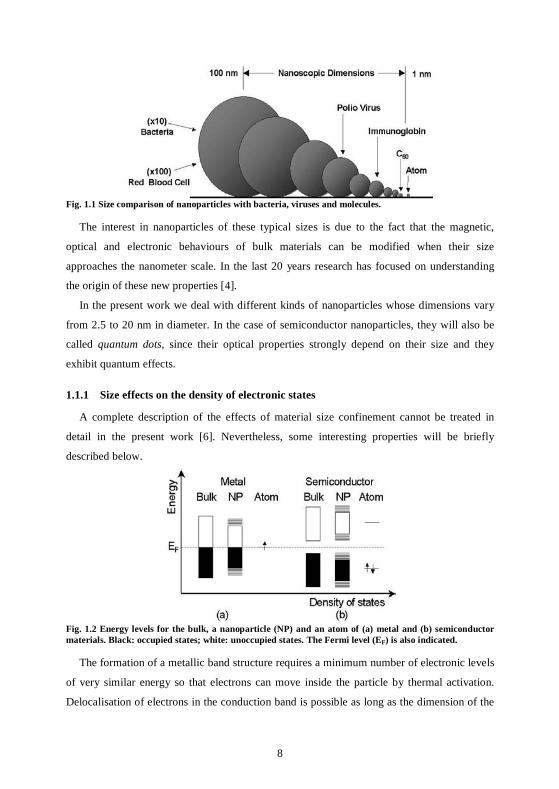
Fig. 1.1 illustrates typical biological objects whose sizes belong to the significant gap existing
between the two regimes, where particles of 1 to 100 nm (made of 10 to 106 atoms) can be
found [3].
8
Fig. 1.1 Size comparison of nanoparticles with bacteria, viruses and molecules.
The interest in nanoparticles of these typical sizes is due to the fact that the magnetic,
optical and electronic behaviours of bulk materials can be modified when their size
approaches the nanometer scale. In the last 20 years research has focused on understanding
the origin of these new properties [4].
In the present work we deal with different kinds of nanoparticles whose dimensions vary
from 2.5 to 20 nm in diameter. In the case of semiconductor nanoparticles, they will also be
called quantum dots, since their optical properties strongly depend on their size and they
exhibit quantum effects.
1.1.1 Size effects on the density of electronic states
A complete description of the effects of material size confinement cannot be treated in
detail in the present work [6]. Nevertheless, some interesting properties will be briefly
described below.
Fig. 1.2 Energy levels for the bulk, a nanoparticle (NP) and an atom of (a) metal and (b) semiconductor materials. Black: occupied states; white: unoccupied states. The Fermi level (EF) is also indicated.
The formation of a metallic band structure requires a minimum number of electronic levels
of very similar energy so that electrons can move inside the particle by thermal activation.
Delocalisation of electrons in the conduction band is possible as long as the dimension of the
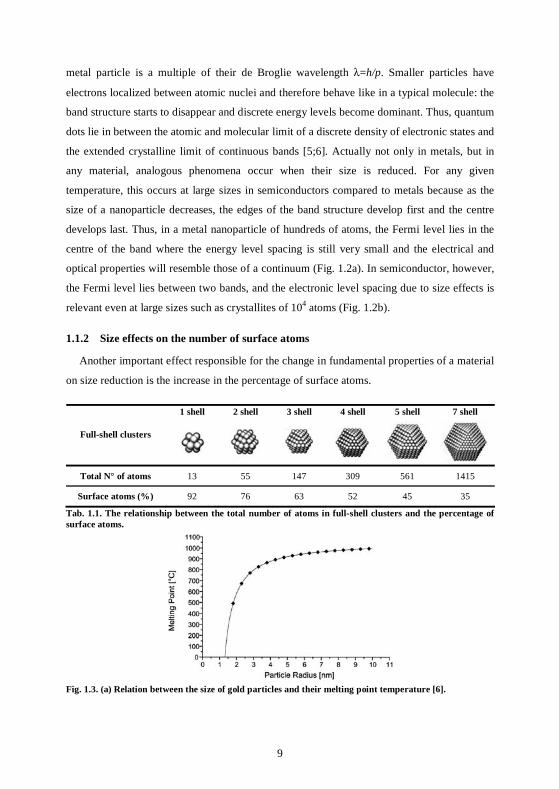
9
metal particle is a multiple of their de Broglie wavelength λ=h/p. Smaller particles have
electrons localized between atomic nuclei and therefore behave like in a typical molecule: the
band structure starts to disappear and discrete energy levels become dominant. Thus, quantum
dots lie in between the atomic and molecular limit of a discrete density of electronic states and
the extended crystalline limit of continuous bands [5;6]. Actually not only in metals, but in
any material, analogous phenomena occur when their size is reduced. For any given
temperature, this occurs at large sizes in semiconductors compared to metals because as the
size of a nanoparticle decreases, the edges of the band structure develop first and the centre
develops last. Thus, in a metal nanoparticle of hundreds of atoms, the Fermi level lies in the
centre of the band where the energy level spacing is still very small and the electrical and
optical properties will resemble those of a continuum (Fig. 1.2a). In semiconductor, however,
the Fermi level lies between two bands, and the electronic level spacing due to size effects is
relevant even at large sizes such as crystallites of 104 atoms (Fig. 1.2b).
1.1.2 Size effects on the number of surface atoms
Another important effect responsible for the change in fundamental properties of a material
on size reduction is the increase in the percentage of surface atoms.
1 shell 2 shell 3 shell 4 shell 5 shell 7 shell
Full-shell clusters
Total N° of atoms 13 55 147 309 561 1415
Surface atoms (%) 92 76 63 52 45 35
Tab. 1.1. The relationship between the total number of atoms in full-shell clusters and the percentage of surface atoms.
Fig. 1.3. (a) Relation between the size of gold particles and their melting point temperature [6].
10
There are some properties that directly depend on the average coordination numbers of the
participating atoms, such as the melting point or the solid-solid phase transition in a crystal.
The melting point of a solid, for example, is reached when the order of the lattice starts to be
lost; as surface atoms have a smaller coordination number, they are easily rearranged. For
typical bulk materials the melting point is a physical constant, but only as long as the surface
is negligibly small in comparison with the total volume. Tab. 1.1 shows that the number of
surface atoms becomes equal or even exceeds that of the inner core atoms on reducing the
crystal size. In this case the melting process starts at a lower temperature (Fig. 1.3).
As a result of the reduction in the number of neighbouring atoms, surface atoms have
narrower d-bands, so that the density of states can vary considerably.
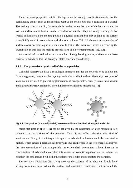
1.1.3 The protective organic shell of the nanoparticles
Colloidal nanocrystals have a solid/liquid interface and, for the colloids to be soluble and
do not aggregate, there must be capping molecules at this interface. Generally two types of
stabilization are used to prevent agglomeration of nanoparticles, namely, steric stabilization
and electrostatic stabilization by steric hindrance or adsorbed molecules [7-8].
(a) (b)
Fig. 1.4. Nanoparticles (a) sterically and (b) electrostatically functionalized with organic molecules.
Steric stabilization (Fig. 1.4a) can be achieved by the adsorption of large molecules, i. e.
polymers, at the surface of the particles. Two distinct effects describe this kind of
stabilization. Firstly, in the interparticle space the adsorbed molecules would be restricted in
motion, which causes a decrease in entropy and thus an increase in the free energy. Moreover,
the interpenetration of the nanoparticle protective shell determines a local increase in
concentration of adsorbed molecules; this causes an osmotic repulsion as the solvent re-
establish the equilibrium by diluting the polymer molecules and separating the particles.
Electrostatic stabilization (Fig. 1.4b) involves the creation of an electrical double layer
arising from ions adsorbed on the surface and associated counterions that surround the
11
particle. Thus, if the electric potential associated with the double layer is sufficiently high, the
Coulombic repulsion between the particles will prevent their aggregation.
Another requirement for good particle stabilization is the use of appropriate solvents. The
stabilizing molecule has to posses a good affinity with the solvent in order to solvate the
particles and form an extended layer for screening the van der Waals attractions between the
particles.
1.1.4 Implications for the miniaturization of electronic devices
In recent years we have witnessed to a continuous process of miniaturization of electronic
devices. If on the one hand we are developing a technology able to product nano-devices, on
the other it is necessary to face the conceptual problems that arise when the dimension of the
electronic components reaches some nanometers: quantum phenomena will increasingly start
to dominate the overall behaviour of such structures and the large surface to volume ratio is
deadly for conventional semiconductor devices.
The electrical conductivity in metals is based on their band structure. As the discrete
energy level structure dominates in nanostructures, Ohm’s law will be no longer valid; we
will be dealing with a very few numbers of charge carriers, if at all, and control of charge and
electrical current on a single electron level will be required. It appears clear therefore that the
miniaturization process towards nano-electronics will not be as natural as it has been for
micro-electronic, but that new concepts need to be developed.
1.2 Bottom-up approaches and self-assembly
Two approaches for the building up of nanoscopic features have been envisaged: the so-
called top-down method and bottom-up methods. In the top down methods, the features are
written directly onto a substrate, for example, by electron beams, and then by applying
appropriate etching and deposition processes, the nanoscopic features are engraved. In the
bottom-up approach, nanocomponents are made from precursors in the liquid, solid, or gas
phase employing either chemical or physical deposition processes that are integrated into
building blocks within the final material structure.
Together with nanoparticles, an impressive variety of nano-building-blocks (e. g. nanorods,
nanocubes, nanotubes, nanowires, etc. [9]), exists and continues to grow with breakthroughs
in synthesis techniques. The application of nanotechnology to areas such as photonics and
electronics, chemical and biological sensors, energy storage, and catalysis requires the
manipulation of these nano-objects into functional materials and devices. Self-assembly
12
[10;11] is generally regarded as the most promising means for designing and controlling the
bottom-up assembly of nanometer-scale objects into structures such as sheets, tubes, wires,
nanoelectronic devices and drug delivery systems.
Over the past century, chemists have invented hundreds of reactions that form and
rearrange the strong bound that results when two atoms share electrons, but it’s only in recent
years that scientists have begun to take advantage of the ability to form looser associations
between small molecules. Nature has exploited these interactions in biorecognition and
biomolecular organization for billions of years. This mechanism governs the assembly of
molecules into living organisms, including for example sewing DNA strands into the familiar
double helix, the properties of liquids, the solubility of solids and the organization of
molecules in membranes. Learning from biology, scientists are now developing highly
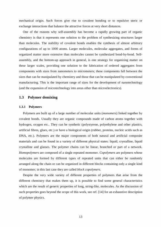
complex systems from components that interact via non-covalent intermolecular forces.
Kind of interaction Free energy of interaction w(r)
charge - charge ∼ - r -1
charge - dipole ∼ - r -2 Electrostatic
charge – non polar ∼ - r -4
dipole - dipole ∼ - r -6
dipole – non polar ∼ - r -6 Van der Waals
non polar – non polar ∼ - r –6 + r -12
Covalent Short range
Hydrogen bond ∼ - r -2
Tab. 1.2. Main physical forces interacting among atoms and molecules and their descriptions in terms of the kind of interaction and the behaviour of the relative free energy of interaction w(r).
Two main kinds of forces control the physical interactions among atoms and molecules:
electrostatic and van der Waals forces (See ref. [12;13] for more detailed insights). Tab. 1.2
gives a schematic description of these forces and other common interaction among atoms,
molecules and ions. We identified the electrostatic forces with those involving one formally
charged specie, but the classification is actually not rigid. Generally speaking, species
presenting a net charge or a dipole can interact among them via coulombic forces, while the
polarization forces arise from the dipole moments induced in atoms and molecules by electric
fields of nearby charges and permanent dipoles. This last kind of interaction is usually found,
for examples, in solvent medium. Moreover, there are forces in nature that have a quantum
13
mechanical origin. Such forces give rise to covalent bonding or to repulsive steric or
exchange interactions that balance the attractive forces at very short distances.
One of the reasons why self-assembly has become a rapidly growing part of organic
chemistry is that it represents one solution to the problem of synthesizing structures larger
than molecules. The stability of covalent bonds enables the synthesis of almost arbitrary
configurations of up to 1000 atoms. Larger molecules, molecular aggregates, and forms of
organized matter more extensive than molecules cannot be synthesized bond-by-bond. Self-
assembly, and the bottom-up approach in general, is one strategy for organizing matter on
these larger scales, providing one solution to the fabrication of ordered aggregates from
components with sizes from nanometers to micrometers; these components fall between the
sizes that can be manipulated by chemistry and those that can be manipulated by conventional
manufacturing. This is the important range of sizes for the development of nanotechnology
(and the expansion of microtechnology into areas other than microelectronics).
1.3 Polymer demixing
1.3.1 Polymers
Polymers are built up of a large number of molecular units (monomers) linked together by
covalent bonds. Usually they are organic compounds made of carbon atoms together with
hydrogen, oxygen etc.. They can be synthetic (polystyrene, polyethylene and other plastics,
artificial fibres, glues, etc.) or have a biological origin (rubber, proteins, nucleic acids such as
DNA, etc.). Polymers are the major components of both natural and artificial composite
materials and can be found in a variety of different physical states: liquid, crystalline, liquid
crystalline and glasses. The polymer chains can be linear, branched or part of a network.
Homopolymers are composed of a single repeated monomer. Copolymers are polymers whose
molecules are formed by different types of repeated units that can either be randomly
arranged along the chain or can be organized in different blocks containing only a single kind
of monomer; in this last case they are called block copolymers.
Despite the very wide variety of different properties of polymers that arise from the
different chemistry that makes them up, it is possible to find some general characteristics
which are the result of generic properties of long, string-like, molecules. As the discussion of
such properties goes beyond the scope of this work, see ref. [14] for an exhaustive description
of polymer physics.
14
1.3.2 Theoretical aspects of polymer phase separation
The study of the behaviour of polymer mixtures has been encouraged historically by the
necessity of combining the properties of the different polymeric components in one material.
In the present work, polymer demixing in blends of immiscible polymers is a route to form
structures on almost every kind of surface and to organize nanoparticles in or on them.
The theoretical model for the behaviour of a polymer mixture was proposed by Flory and
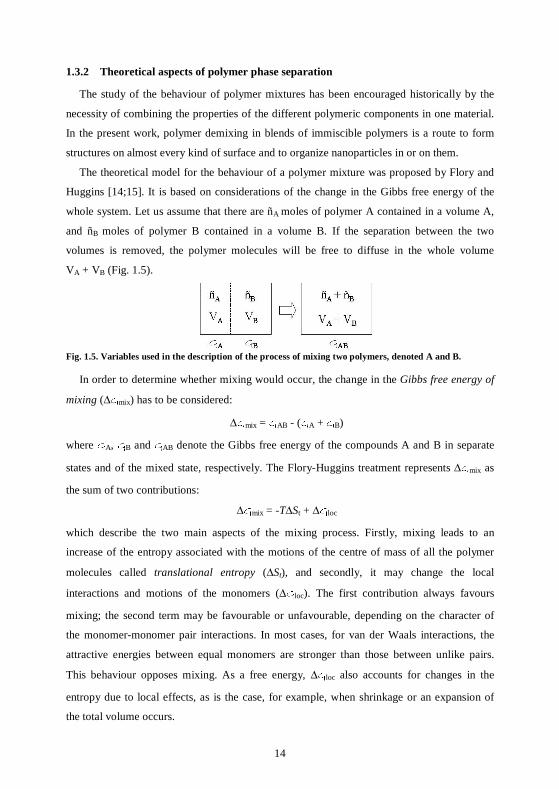
Huggins [14;15]. It is based on considerations of the change in the Gibbs free energy of the
whole system. Let us assume that there are ñA moles of polymer A contained in a volume A,
and ñB moles of polymer B contained in a volume B. If the separation between the two
volumes is removed, the polymer molecules will be free to diffuse in the whole volume
VA + VB (Fig. 1.5).
Fig. 1.5. Variables used in the description of the process of mixing two polymers, denoted A and B.
In order to determine whether mixing would occur, the change in the Gibbs free energy of
mixing (∆Gmix) has to be considered:
∆Gmix = GAB - (GA + GB)
where GA, GB and GAB denote the Gibbs free energy of the compounds A and B in separate
states and of the mixed state, respectively. The Flory-Huggins treatment represents ∆Gmix as
the sum of two contributions:
∆Gmix = -T∆St + ∆Gloc
which describe the two main aspects of the mixing process. Firstly, mixing leads to an
increase of the entropy associated with the motions of the centre of mass of all the polymer
molecules called translational entropy (∆St), and secondly, it may change the local
interactions and motions of the monomers (∆Gloc). The first contribution always favours
mixing; the second term may be favourable or unfavourable, depending on the character of
the monomer-monomer pair interactions. In most cases, for van der Waals interactions, the
attractive energies between equal monomers are stronger than those between unlike pairs.
This behaviour opposes mixing. As a free energy, ∆Gloc also accounts for changes in the
entropy due to local effects, as is the case, for example, when shrinkage or an expansion of
the total volume occurs.

15
The increase in the translational entropy is described by:
BBAAB
BA
At nn
V
Vn
V
Vn
R
S φφ ln~ln~ln~ln~ −−=+=∆
where φA and φB represent the volume fractions of the two components in the mixture
(φA + φB = 1), and R is the perfect gas constant.
The change in the local interactions is expressed by the equation:
∆Gloc BAcv
VRT φχφ=
where νc denotes the molar volume of a reference unit common to both polymers (e. g. the
monomeric units), while χ is the so called Flory-Huggins parameter, which is dimensionless
and determines in an empirical manner the change in the local free energy per reference unit.
The resulting Flory-Huggins formulation for the Gibbs free energy of mixing of polymer
blend is:
∆Gmix ⎟⎟⎠
⎞⎜⎜⎝
⎛++=⎟⎟
⎠
⎞⎜⎜⎝
⎛++= BAB
B
BA
A
AcBA
cB
B
BA
A
A
NNnRT
vvvRTV φχφφφφφφφχφφφφ
lnln~lnln
where it was introduced:
A
AA n
Vv ~φ
= ; B
BB n
Vv ~φ
= ; c
c v
Vn =~ ;
c
AA v
vN = and
c
BB v
vN = .
ñc is the number of moles of the reference unit, νA and νB the molar volumes of the polymers
A and B. Choosing the same monomeric unit of volume νc for both the polymers, NA and NB
express the degrees of polymerization of the polymers A and B.
The Flory-Huggins equation provides the basis for a general discussion of the miscibility
properties of a pair of polymers. A necessary requirement for mixing is the decrease of the
Gibbs free energy. The entropic contribution to the Gibbs free energy of mixing is always
negative, favouring the mixing; on the other hand ∆St is extremely small in polymers due to
the typical high molecular weights of their molecules (νA, νB → ∞); thus the critical parameter
in this case is the χ-parameter:
• If the χ-parameter is negative or zero, then mixing takes place.
• If the χ-parameter is positive, then the enthalpic contribution opposes the mixing and
no conclusion can be reached a priori. For example Fig. 1.6a shows a case where the χ-
parameter, and thus the enthalpic contribution, is positive. The Gibbs free energy
variation can be both positive and negative depending on φA.

16
-0,4
-0,2
0
0,2
0,4
0,6
0,8
1
0 0,2 0,4 0,6 0,8 1φ Α
∆G
mix
/(RT
n c/N
)entropic A entropic B
enthalpic total
(a)
-0,3
-0,25
-0,2
-0,15
-0,1
-0,05
0
0,05
0 0,2 0,4 0,6 0,8 1φ Α
∆G
mix/(
RT
n c/N
)
N
S
χ N = 2.8
χ N = 2.4
χ N = 2.0
χ N = 1.6
(b)
-0,15
-0,1
-0,05
0
0 0,2 0,4 0,6 0,8 1φ Α
∆G
mix/(
RT
n c/N
)
xN=2.4
φA' φA''
K
J
(c)
0
2
4
6
8
10
0 0,2 0,4 0,6 0,8 1φ Α
χN
bimodal linespinodal line
homogeneous phase
two-phase structure
(d)
Fig. 1.6. (a) Entropic and enthalpic contributions to the Gibbs free of mixing in the case NA=4NB=4N and χN=2.8. (b) Gibbs free of mixing in the case NA=NB=N and different values of χN. (c) Demixing mechanism. (d) Binodal and spinodal lines in the case NA=NB=N.
Fig. 1.6b shows the change in the Gibbs free energy of mixing for different values of the χ-
parameter in the simplified case NA = NB = N. Depending on the χ-parameter, the curves alter
their shape and above a critical value a maximum between two minima appears. Referring to
Fig. 1.6c, let us suppose we have a polymer blend with an initial relative concentration
polymer-A/polymer-B 30/70 (φA = 0.3) and a value χN = 2.4. The arrow K indicates that a
homogeneous mixing of A and B would lead to a decrease of ∆Gmix, when compared to two
separate one-components (∆Gmix = 0). However, as shown by the arrow J, the Gibbs free
energy can be further reduced, if a two-phase structure is formed again, now being composed
of two mixed phases, with composition φA′ and φA″. This further decrease of ∆Gmix is only
possible for φA′ ≤ φA ≤ φA″ (miscibility gap). The boundary between the one-phase and the
17
two-phase region is called bimodal line and is determined by the compositions φA′ and φA″ of
the equilibrium phase with minimum Gibbs free energies in the miscibility gap (Fig. 1.6d); in
the general case the points of the bimodal line can be determined by the construction of the
tangent to the two minima of the curve of the Gibbs free energy variation.
In this work we are dealing with polymer blends at room temperature, which undergo
solvent evaporation. Thus, we are actually dealing with a system made of three components:
the two polymers and the solvent. These kinds of system have been treated in literature and it
is demonstrated that demixing in a two polymer phases will arise only when the polymer
molecules are present in a certain range of proportions and concentrations [16]. For a diluted
polymer solution the monomer interaction will be low, with χ→ 0. Solvent evaporation
results in a decrease of the free volume available for local motion of the monomers, lowering
their entropy, while the average monomer spacing diminishes, making them interact. Thus,
solvent evaporation can be described by an increase of χ and thus the transformation, under
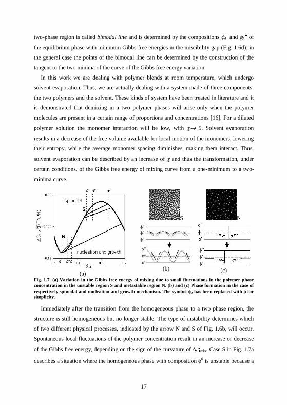
certain conditions, of the Gibbs free energy of mixing curve from a one-minimum to a two-
minima curve.
(a)
S N
(b) (c)
Fig. 1.7. (a) Variation in the Gibbs free energy of mixing due to small fluctuations in the polymer phase concentration in the unstable region S and metastable region N. (b) and (c) Phase formation in the case of respectively spinodal and nucleation and growth mechanism. The symbol φA has been replaced with φ for simplicity.
Immediately after the transition from the homogeneous phase to a two phase region, the
structure is still homogeneous but no longer stable. The type of instability determines which
of two different physical processes, indicated by the arrow N and S of Fig. 1.6b, will occur.
Spontaneous local fluctuations of the polymer concentration result in an increase or decrease
of the Gibbs free energy, depending on the sign of the curvature of ∆Gmix. Case S in Fig. 1.7a
describes a situation where the homogeneous phase with composition φ0 is unstable because a
18
small separation in composition φ+ and φ- lowers the free energy; such separations occur
spontaneously and then increase until the lowest Gibbs free energy is achieved, which is the
usual condition given by the tangent to the curve. During this process the amplitude of the
concentration fluctuations increases and the direction of the flow of the A-chains is towards
A-rich regions, as indicated by the arrows in Fig. 1.7b. This region delimited by the two
inflection points is called spinodal line and its boundary is indicated in Fig. 1.6d with the
dashed line.
Case N in Fig. 1.7a represents a metastable phase: small separations in composition all
increase the free energy, but a large composition changes can decrease it. Since small
fluctuations decay, the only way to achieve a decrease in the free energy is a large fluctuation
which leads directly to the formation of a nucleus with the new equilibrium phase with
composition φ″ (Fig. 1.7c). After it has formed it increases in size, with a flux of the A-chains
towards A-poor regions, until equilibrium is achieved. This process is called nucleation and
growth. Fig. 1.7b and c are pictures of typical phase structures resulting respectively from
spinodal decomposition and nucleation and growth behaviour of the polymer blend.
1.3.3 Phase separation in block copolymers
Although the covalent bonds that link the blocks in a block copolymer molecule inhibit
phase separation process, micro-phase separation still takes place leading to different classes
of ordered structures depending on the ratio between the degrees of polymerisation. Fig. 1.8
shows the phase separation diagram for diblock copolymers. For NA << NB spherical
inclusions of A chains in a B-matrix are formed, forming a body-centred cubic lattice. For
larger values of NA (but still NA < NB) the A-domains have a cylindrical shape and are
hexagonally arranged. A layered structures forms under symmetrical conditions (NA ≈ NB),
while for NA > NB the phases are inverted and the A-blocks now constitute the matrix. Under
special conditions a periodic structure occurs (gyroid) in which both phases are continuous.
The lower area of the phase diagram of Fig. 1.8 corresponds to a homogeneous or
disordered phase, analogous to that observed in Fig. 1.6d. However, the line that separates the
homogeneous phase region from the two-phase region does not represent a bimodal line,
because block copolymer melts are a one-component systems and the line therefore describes
a phase transition rather than a miscibility gap. It is interesting to observe that the
homogeneous phase has a larger stability range when compared with a binary symmetric
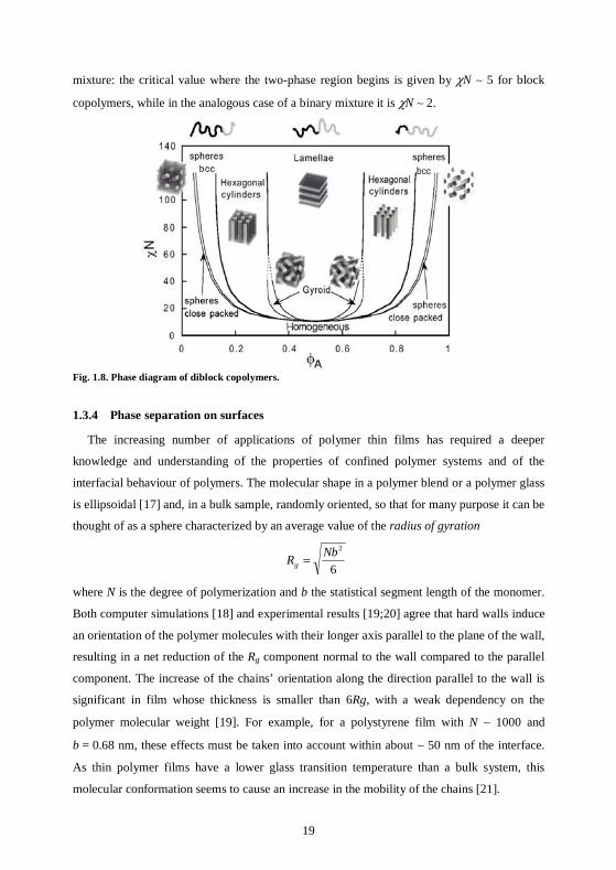
19
mixture: the critical value where the two-phase region begins is given by χN ∼ 5 for block
copolymers, while in the analogous case of a binary mixture it is χN ∼ 2.
Fig. 1.8. Phase diagram of diblock copolymers.
1.3.4 Phase separation on surfaces
The increasing number of applications of polymer thin films has required a deeper
knowledge and understanding of the properties of confined polymer systems and of the
interfacial behaviour of polymers. The molecular shape in a polymer blend or a polymer glass
is ellipsoidal [17] and, in a bulk sample, randomly oriented, so that for many purpose it can be
thought of as a sphere characterized by an average value of the radius of gyration
6
2NbRg =
where N is the degree of polymerization and b the statistical segment length of the monomer.
Both computer simulations [18] and experimental results [19;20] agree that hard walls induce
an orientation of the polymer molecules with their longer axis parallel to the plane of the wall,
resulting in a net reduction of the Rg component normal to the wall compared to the parallel
component. The increase of the chains’ orientation along the direction parallel to the wall is
significant in film whose thickness is smaller than 6Rg, with a weak dependency on the
polymer molecular weight [19]. For example, for a polystyrene film with N ∼ 1000 and
b = 0.68 nm, these effects must be taken into account within about ∼ 50 nm of the interface.
As thin polymer films have a lower glass transition temperature than a bulk system, this
molecular conformation seems to cause an increase in the mobility of the chains [21].
20
As the thickness of a film decreases, the surface-to-bulk ratio increases and the average
number of neighbour molecules diminishes. For polymer blends, the Flory-Huggins
interaction parameter χ should be corrected by taking into account the reduced number of
interactions [22]. Moreover, depending on the interaction between the substrate and the
polymer molecules, the latter may adsorb on the surface, resulting in a reduced mobility of the
polymer chains at the surface (with the subsequent reduction of the glass transition
temperature [23]), and an induced variation of the polymer concentration profile along the
thickness of the film. This last effect affects the demixing behaviour of polymer blends in thin
polymer films compared to bulk systems [24;25]. The properties of the film will depend on
the specific interaction of the polymers with the substrates or with the air-interface and a
theoretical treatment of the system in general terms becomes difficult. This substrate-polymer
interaction can be used under certain conditions to induce an order in the polymer phase
structures arising from the demixing [26].
For block copolymers, the presence of an interface can affect the orientation of the
microdomains [27]. The polymer phase structure is the result of the equilibrium between the
energetically favourable separation of the blocks, the entropically unfavourable stretching of
the individual blocks and the minimization of the interfacial energy at the polymer/substrate
or polymer/air boundary. Laterally-oriented microdomain structures can appear at the surface
when one of the blocks is strongly adsorbed on the substrate and the polymer film thickness is
comparable with the periodicity of the structure (e. g. the lamella periodicity for symmetric
block copolymers). In this case, the adsorbed block (A, say) forms a tightly bound monolayer
on the surface, while the conformation of the other block (B) depends on different parameters:
if the compatibility of the B monomers with air is poor, individual B chains will collapse
forming either surface spherical micelles or a ribbon structure (cylindrical rods lying on the
surface) of B blocks. The type of surface structure depends on the relative lengths of the
blocks and the interaction parameters, apart from some experimental parameters. In the strong
segregation regime (χN >> 10) the free energy of a micelle (a ribbon) is [28]:
Bel
Aelsurfd FFFF ++=
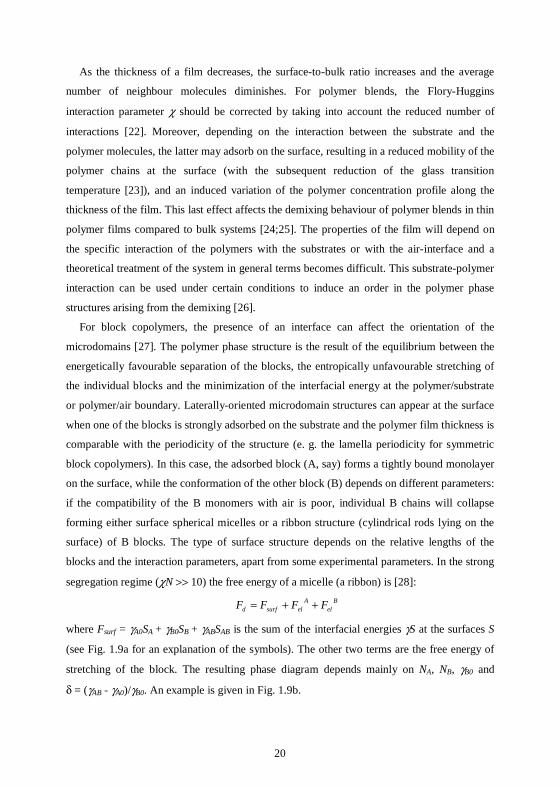
where Fsurf = γA0SA + γB0SB + γABSAB is the sum of the interfacial energies γS at the surfaces S
(see Fig. 1.9a for an explanation of the symbols). The other two terms are the free energy of
stretching of the block. The resulting phase diagram depends mainly on NA, NB, γB0 and
δ = (γAB - γA0)/γB0. An example is given in Fig. 1.9b.
21
(a) (b)
Fig. 1.9. (a) Schematic representation of a micelle on a surface. (b) Phase diagram of a A-b-B diblock copolymer with A blocks strongly adsorbed on the substrate for γB0 = γ = 0.1 and δ = (γAB-γA0)/γB0 = -0.5 [28].
For thicker layer, under equilibrium conditions, symmetric diblock copolymers form
lamellar microdomains characterized by a typical periodicity L0. When both the interfaces
attract the same block the film thickness is given by t = nL0, where n is an integer number.
When the two boundary surfaces have a better affinity with different blocks, flat films are
found for t = (n + 0.5)L0. Deviations from these quantized values lead to surface relief
structures that appear on top of the flat film [29].
1.3.5 Phase separation of particle filled systems
The introduction of hard spheres in a polymer blend corresponds in a certain way to the
introduction of new polymer/hard wall interfaces. It is thus expected that some of the
phenomena observed for phase separation on surfaces will be present in particle-filled
polymer systems.
Vacatello [30] performed computer simulations on polymer systems filled with particles of
a size comparable to the polymer chains and found that the polymer units at the interface of
the filler particles were arranged in densely packed and ordered shells analogous to the layers
found near planar solid surfaces. Even in the absence of specific interactions with the
polymer, the filler particles behaved as highly functional physical cross-links, reducing the
overall mobility of the polymer chains with respect to the unfilled melt. For a given volume
fraction of filler, this effect was more pronounced when the particles were smaller. The
conformational distribution of the polymer was strongly perturbed by the presence of the filler
both on the global and on the local scale. In particular, the average dimensions of chain
segments comprising more than a few units was reduced when compared to the unfilled melt.
22
Although the systems simulated by Vacatello were characterized by relatively short
polymer chains (N ∼ 100) and large particles (diameters from 10 to 16 times the statistical
segment length of the polymer) with a high particle volume fraction (∼ 33 %), his results
nevertheless give an indication of the phenomena arising in polymer/nanoparticle composite
systems.
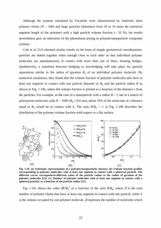
Cole et al. [31] obtained similar results on the basis of simple geometrical considerations:
particles are linked together when enough close to each other so that individual polymer
molecules are simultaneously in contact with more than one of them, forming bridges.
Qualitatively, a transition between bridging to non-bridging will take place for particle
separations similar to the radius of gyration Rg of an individual polymer molecule. By
numerical simulation, they found that the volume fraction of polymer molecules that have at
least one segment in contact with one particle depends on Rg and the particle radius R as
shown in Fig. 1.10b, where the volume fraction is plotted as a function of the distance z from
the particles. For example, in the case of a nanoparticle with a radius R = 2 nm in a matrix of
polystyrene molecules with N ∼ 1000 (Rg = 8.6 nm), about 10% of the molecules at a distance
equal to Rg would be in contact with it. The ratio R/Rg = ∞ in Fig. 1.10b describes the
distribution of the polymer volume fraction with respect to a flat surface.
(a)
(b)
(c) Fig. 1.10. (a) Schematic representation of a polymer/nanoparticles mixture. (b) Volume fraction profiles corresponding to polymer molecules with at least one segment in contact with a spherical particle. The different curves correspond-to-different ratios of the particle radius to the radius of gyration of the polymer molecules [31]. (c) Number of polymer molecules with at least one segment in contact with a spherical particle, as a function of the particle radius [31].
Fig. 1.10c shows the value βV/Rg3 as a function of the ratio R/Rg, where β is the total
number of polymer chains that have at least one segment in contact with one particle, while V
is the volume occupied by one polymer molecule. β expresses the number of molecules which
23
are able to link a given particle with its neighbours by the formation of the bridge and has the
expression:
2
36.143.13
⎟⎟
⎠
⎞
⎜⎜
⎝
⎛+
⎟⎟
⎠
⎞
⎜⎜
⎝
⎛=
gggR
R
R
R
R
Vβ
In the previous example (the density of polystyrene is 1.05 g/cm2) β takes the value of ∼ 15.
Although the limitations deriving from simple geometrical assumptions which do not take
into account possible interactions between the polymer molecules and the particles or
problems arising from the reduced particles surface in the limit R → 0 (which determines the
number of available contact site), a schematic picture of the local situation of a system of
particles and polymer molecules is given.
1.4 Aim of the work
Nowadays there is a need to learn how to manipulate nanosized particles and form the
ensemble into periodically ordered particulate materials for application into devices making
use of the special physical properties that arise due to the nanometric crystallite sizes, like the
quantum effects, for example. Designing finite mesostructures with a given geometry is the
future challenge to make use of the special properties of nanoparticles for applications.
Ordered assemblies of nanometer-sized particles are thus an interesting class of nanomaterials
that have exceptional potential to achieve one-two- and three-dimensional structures for a
wide variety of applications ranging from photonic devices to memory devices, two-
dimensional arrays of magnetic nanoparticles [32], or single-electron microelectronic devices,
amongst others [33].
The aim of this work is the organization of different kinds of nanoparticles in ordered
surface structures. The building blocks of these structures are nanoparticles and polymeric
molecules, whose synthesis and property description will not be treated. Some of the
collective physical properties of polymer and composite polymer/nanoparticle systems were
studied. The main effort was dedicated to develop bottom-up techniques for the organization
of the nanoparticles on micrometer, sub-micrometer, nanometer, and multiple length scales.
Top-down techniques, such as soft-lithography techniques, were used to push self-organized
structures towards a higher level of order or a multiple length scale design.
An elegant method to organize nanometric particles is by self-assembly, often inspired by
nature. All of the techniques used and developed in this work were concerned with
overcoming the intrinsic limitations of such powerful techniques as, for example,

24
photolithographic methods. In spite of their spectacular successes, they have certain
drawbacks that limit their applicability to new devices and fields of studies:
• they can not be used with the many organic and biological materials that are
incompatible with typical photoresist and processes;
• as the minimum feature size depends on the source light wavelength and on the
numerical aperture of the optical system, a point will be reached where optical
lithography can no longer reduce the feature sizes [34];
• the substrate is usually patterned sequentially and therefore the patterning time
scales linearly with the area to be patterned;
• they have difficulties in forming features on curved, uneven, or rough objects;
• they can only directly pattern a small set of specialized materials;
• they can not reproduce features with complex, three dimensional shapes;
• they require expensive capital equipment and infrastructures.
Although bottom-up techniques such those presented in this work are still far from having
the topographical precision and reproducibility of photolithographic methods, they do not
present the problems listed above. In addition, self-organizing systems allow the creation of
even complex structures in few elementary processing steps, with a remarkable reduction of
time and infrastructure compared to lithographic techniques.
Polymeric molecules are ideal building blocks for techniques with the characteristics
described above. This is the reason why we have decided to use homopolymer and block
copolymer self-organizing phase properties to create templates for the organization of
nanoparticles. Working with polymers presents several advantages:
• a large variety of environmentally friendly and bio-compatible polymers is
available on the market;
• they can be chosen to be soluble in water or in organic solvents depending on the
experimental requirements;
• they present self organizing properties and the typical structure length scale can
vary from the micrometer (homopolymer phase separation) to the nanometer
(block-copolymer self assembly);
• their structure sizes and morphologies can be controlled by several experimental
parameters;
• the patterning by phase separation takes place almost simultaneously over the entire
surface, eliminating the effect of size on processing time;
25
• they can be combined with soft lithographic techniques, such as micro-contact
printing [35], capillary rise [36] or other top-down methods;
• many kind of substrates can be coated with polymers, irrespective of the material
and the shape;
• they are generally low cost materials and easily purchased.
The introduction of nanoparticles in combination with the polymeric templates is done in
tune with the general principle of simplicity of bottom-up approaches: nanoparticles are mixed
with the polymer solution or adsorbed to the polymer structures and spontaneously self-
organize via non-covalent interactions.
The present work reports on strategies for the organization of nano-sized objects that have
been previously synthesized. This means that a very wide range of objects can be used, such
as metallic, semiconductor nanoparticles or even organic molecules.
1.5 State of the art
In recent years the synthesis and study of inorganic nanoparticles has become a major
interdisciplinary research area, resulting from their numerous applications in various fields.
For example, the change in the absorption properties with size in metal particles has found
applications in colouring transparent materials since ancient times [37]. However, the range of
colours and their nuances have been considerably extended up to the present time, as the
ability to control the size and the separation of metal nanoparticles has increased [38].
Research on semiconductor nanoparticles with size-dependent optical properties and
electronic properties is motivated by potential uses in the fields of non-linear optics [39], light
emitting devices and display devices [40], solar cells [41], biological labels (see below),
electronics [42], catalysis [43], among others [44].
1.5.1 Semiconductor nanoparticles are ideal biological labels
Semiconductor nanoparticles have attractive photoluminescence properties that have
stimulated interest in their use as a new class of biological labels with properties and
applications that are not available with traditional organic dyes and fluorescent proteins [45].
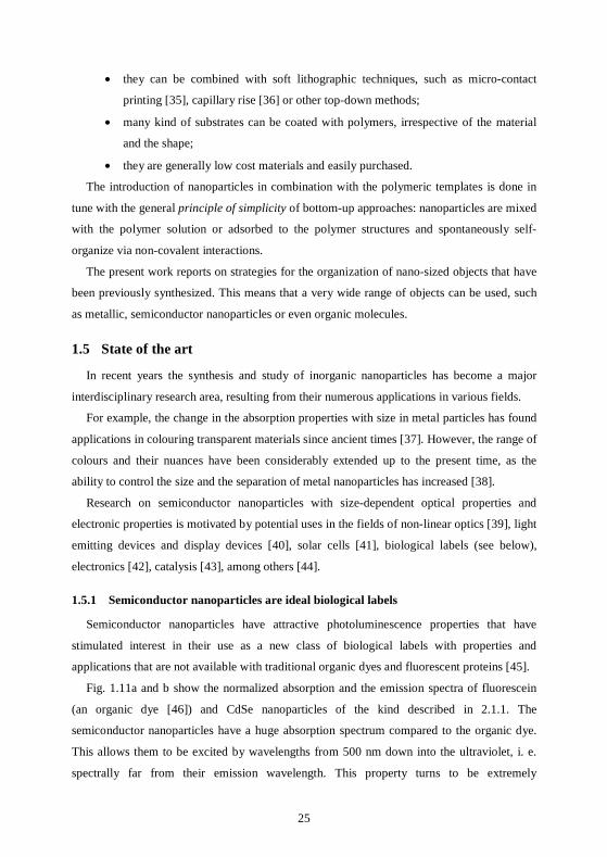
Fig. 1.11a and b show the normalized absorption and the emission spectra of fluorescein
(an organic dye [46]) and CdSe nanoparticles of the kind described in 2.1.1. The
semiconductor nanoparticles have a huge absorption spectrum compared to the organic dye.
This allows them to be excited by wavelengths from 500 nm down into the ultraviolet, i. e.
spectrally far from their emission wavelength. This property turns to be extremely
26
advantageous for practical applications because it allows efficient filtering of exciting
radiation, without affecting emission detection.
Multicolour analysis with different dyes requires multiple excitation sources and
multiplexed channels recorded simultaneously; this greatly increases the complexity of the
detection systems [47]. To simplify microarray systems and analysis, multiple labelling
applications need an alternative technology to organic fluorophores. Quantum dots could
potentially be this technology. The quantum dot emission spectrum is narrower than that of
the fluorescein molecules (Fig. 1.11) and its central wavelength can be tuned with the
nanoparticles size (Fig. 2.1b). Nanocrystals with different sizes can be excited with a single
radiation wavelength, resulting in many emission colours that can be detected simultaneously
[48].
(a)
(b)
Fig. 1.11. Absorption and emission spectra of (a) Fluorescein organic molecules [46] and (b) CdSe nanoparticles of 2.5 nm in diameter.
Another important property of nanoparticles is their low photo-degradation compared to
organic dyes, which makes them particularly suitable for in vivo experiments [48;49].
Synthetic fluorophores or fluorescent proteins are currently used as tracers for in vivo
imaging, but these approaches are restricted by photo-bleaching and the limited availability of
different colours. Dubertret et al. [50] demonstrated that CdSe nanocrystals encapsulated in
phospholipid block copolymer micelles could be used in lineage-tracing experiments in
embryogenesis. Moreover the nanoparticles were found to be stable, non-toxic and slow to
photo-bleach when injected into early-stage embryos. Similarly, Dahan et al. [51] observed
the lateral dynamics of individual glycin receptors tracked with quantum dots in the neuronal
membranes of living cells for periods ranging from milliseconds to minutes. Moreover, the
27
quantum dots, being suitable for TEM imaging, provided information on the precise
localization of diffusing glycin and demonstrated access into the core of the synapse.
One of the main questions that has to be solved for future developments of cell-labelling
techniques based on semiconductor quantum dots is that of their toxicity. CdSe nanoparticles,
for example, were found to be toxic under certain condition due to the release of free Cd ions
during surface oxidation [52]. However, surface coatings such as ZnS and BSA were shown
to significantly reduce their cyto-toxicity. In general, the use of quantum dots in in vivo
experiments must be critically examined because they could induce cell death because of their
inherent chemical composition, although novel mechanisms of toxicity due to their size.
The biological application of quantum dots is also limited by problems in surface
chemistry. Semiconductor nanocrystals can be grown directly in aqueous solutions [53;54],
but their size distribution and quantum yield are in general poorer than those of particles
grown in organic surfactants. To make organically synthesized particles water-soluble, the
surface species are generally exchanged with monolayers made of bifunctional molecules
[49;55]. Alternatively, a glass shell may be grown around the nanoparticle. Modification of
silica surface with different groups has been used to control the interaction of the
nanoparticles with the biological sample [48;56]. However, these capping techniques
generally produced quantum dots which tended to aggregate and adsorb non-specifically.
Many efforts have been made during last years to face these problems [57]. Recently Bäumle
et al. [58] demonstrated the synthesis of CdSe nanoparticles with high fluorescence quantum
yield directly in water; glutathione was used as a stabilizing agent while the quantum dots
were coated with streptavidin for application as fluorescent probes.
A further peculiarity of semiconductor nanoparticles with respect to common fluorophores
is their long fluorescence lifetime. This thematic will be discussed in ch. 3.
1.5.2 Nanoparticles within polymers
Numerical simulations of phase-separating binary fluids, such as polymer blends, have
found that small (nanometer-sized) mobile particles with a selective affinity for one of the
phases will be concentrated into this phase during demixing [59;60]. This partitioning of the
particles into one of the two polymer phases is analogous to the partitioning of chemical
species in immiscible two-phase solvent systems, often used by chemists as a purification
method [16]. A few authors have studied the distribution of nanoparticles in block copolymer
films. These systems are quite similar to nanoparticles in demixed polymer films, but with
two significant differences: the block copolymer/nanoparticle films are much more ordered
28
systems and are much closer to thermodynamic equilibrium than demixed homopolymer films
[61;62]. In addition to the partitioning of the nanoparticles in one of the film phases, there
may be an enrichment of the nanoparticles at the polymer interfaces. This effect has been
described in numerical simulations of both homopolymer blends and block copolymer films
containing nanoparticles [59;61]. The particles accumulate at the interfaces between the
different polymers when their presence reduces the interfacial energy of the system, as is the
case for particles with similar energies of interaction for both polymer phases. Alternatively,
the nanoparticles may accumulate at the interface if their movement across the interface in the
film is hindered.
Polymer/nanoparticle composite films are used today in different fields of technology. One
example is the development of hybrid nanocrystal-organic solar cells. Techniques based on
polymer layers instead of Si allow for the manufacturing of ultra-thin flexible devices. The
mixing of the nanoparticles into a polymer medium allows the creation of charge transfer
junctions with high interfacial area. Solar cells based on polymer/nanocrystal composite
blends have been demonstrated to have promising performances for the development of low
cost solar cell devices [41].
Metal nanoparticles have been used as catalysts on conductive polymer supports and their
influence on electrochemical reactions has been investigated [63]. Recently, it has been
demonstrated that conductive polymer films containing Pd nanoparticles showed enhanced
redox current and discharge capacity for polymer lithium battery devices. The enhanced
activity is attributed to the nanosize dispersion of the nanoparticles within the polymer [64].
Nowadays there is a great interest in the possibility of employing magnetic nanoparticle
assemblies as recording media for extremely high-density magnetic hard disk drives [65].
However, before potential applications can be considered, it is necessary to develop a low-
cost technology capable of producing ordered and addressable features of magnetic domains.
Thus, it is necessary to develop a technique to organize the nanoparticles in a material suitable
to be processed while keeping their chemical integrity and thus their magnetic properties.
Recently, Mn12 clusters were inserted into mesoporous silicates [66] with pore diameters from
2.5 nm to 10 nm. Although the molecular magnets were organized and isolated from each
other by immobilizing the clusters in the channels of the mesoporous materials, no control of
the inter-cluster distance was achieved. An alternative approach to isolate the magnetic
clusters from each other is their incorporation in organic polymers [67]. Inorganic–organic
hybrid polymers starting from molecular clusters capped by polymerizable organic groups
29
were developed [68]; the clusters act as cross-linking centres via polymerization of their shell
with the polymer molecules.
1.5.3 Lateral organization of nanoparticles
A number of different methods for the organization of pre-synthesized nanoparticles or
other sub-micron and nano-scale objects on surfaces have been reported [8]. These include the
use of optical tweezers to individually position nanoparticles [69] or of charge-charge
interactions to allow the building up of polyelectrolyte/nanoparticle layer structures and thus
the 3D organization of nanoparticles within polymer layers [70].
Capillary forces on particles have been used to obtain ordered aggregates of nanoparticles.
If a droplet of the colloid suspension is dried slowly on an unpatterned polar surface, the
particles aggregate at the rim of the droplet because of attractive capillary forces between the
particles when the water film thickness is of the dimensions of the particle diameter.
Positioning and adhesion in the suspension liquid are controlled by charge and polar
interactions between the substrate and particle surfaces. Thus, capillary forces between the
particles and the surface laterally displace the particles during drying. After complete
evaporation an irreversible reorganization of the particle-substrate interface occurs. Dewetting
of colloidal dispersions from contoured surfaces, attractive capillary forces and geometric
templating can be combined to provide an attractive method of assembling colloidal particles
into complex aggregates. When an aqueous dispersion of colloidal particles is allowed to
dewet from a patterned solid surface with appropriate relief structures, the particles get
trapped and assemble into aggregates whose structures are determined by the geometric
confinement provided by the templates. By this method, the capability and feasibility of
assembling polystyrene beads and silica colloids (∼150 nm in diameter) into complex
aggregates have been demonstrated [71].
Colloidal particles can be trapped at a liquid surface as a result of the electrostatic and
surface tension forces. The interaction between the ions/macromolecules in solution and
charged lipid Langmuir layers drives the organization at the air-water interface. The
nanoparticles organized in this fashion by the Langmuir-Blodgett method can then be
transferred onto suitable substrates [72]. The surfaces of these colloidal spheres are modified
such that they will only be partially immersed into the surface of a liquid after they have been
spread onto the air-liquid interface [73]. It is the strong attractive interactions between the
colloidal spheres that lead to the spontaneous formation of a 2D aggregate at the interface.
30
Extended ordered aggregates of nanoparticles of this kind have been realized via strict control
of the experimental parameters [74].
During recent years, numerous template-assisted techniques for the lateral organization of
the nanoparticles have been developed. Self-organization on chemically patterned surfaces
can be achieved in a rather straightforward way by the use of charged surfaces, as the
nanoparticles in suspension are most often charged to prevent coagulation. Substrates are
patterned by molecular layers in mesoscale dimensions. Substrates for such chemisorption are
usually gold surfaces regiospecifically modified with functionalized thiol molecules by
microcontact printing [75] or silica surfaces that have been photo-patterned by a preadsorbed
cationic monomer [76]. However, only moderate packing density of the particles is achieved
due to their mutual repulsion [77]. One way to overcome this problem is the application of
cationic surfactants that increase the charge shielding and, due to adsorption onto the particle
surface, introduce attractive forces such as van der Waals interaction [78]. In one example,
micro-contact printing of charged species was used to create sites for the selective
nanoparticle adsorption [79].
Periodic arrangements of gold nanoclusters were produced on graphite surfaces having
organized nanodefects created by focused ion beam techniques [80]. Alternatively, the
selective deposition of CdSe nanocrystals onto organic channel-like templates fabricated by
Langmuir-Blodgett technique was achieved by anisotropic dewetting of the nanocrystal
solvent [81].
Biological molecules have also been used as templates, for example oligonucleotides and
their analogues have been used as templates, to electrostatically encapsulate cationic-capped
gold nanoparticles [82]. Protein molecules have the ability to build nanometer sized
supramolecules by self-assembly, which can themselves create higher order structures like
cell components. Mirkin et al. [83] and Alivisatos et al. [84] have shown that complementary
DNA oligonucleotides offer possibilities for self-assembled nanoparticles. The concept of
DNA hybridization-based self-organization of molecular compounds has been applied to the
assembly of DNA-derivatized gold colloids [83;84;85] and the fabrication of 3D particle
structures [86].
Application of an electric field results in structural transitions in the colloidal suspension
because the interparticle electrostatic interactions due to polarization are stronger than
Brownian forces. The tendency of particles in suspension to form structures such as chains
upon application of an electric field was reported centuries ago [87]. Recently, it was
demonstrated that at low fields, where the interparticle electrostatic interaction energies are
31
low compared to thermal energies, no significant particle association is generally observed
and the nanoparticles tend to sediment to the bottom electrode, if their density is higher than
the solvent density. However, at field strengths ~1000 V/mm, field-induced structures, such
as chains of touching particles, are formed that do not break up due to thermal fluctuations,
implying that the electrostatic energy at contact was many times kT [88].
The variety of structures available using self-assembled block copolymer films, the
tunability of the scale, shape and periodicity of their domains with their molecular weight,
together with the tendency of metals of selective decorating one phase of the film, make block
copolymers ideal templates for the lateral organization of the nanoparticles. Zehner et al. [89]
described an extremely simple and effective technique for the selective decoration of a phase
separated block copolymer film with thiol passivated gold nanocrystals. A photonic crystal
with improved dielectric contrast was made by selective deposition of CdSe nanocrystals to
one domain of a self-assembled triblock copolymer [90]. Recently, Bockstaller et al. [91]
demonstrated a hierarchically patterned nanostructure of ternary mixtures of two different-
sized nanoparticle species (gold and silica) and a block copolymer by strategic design of the
size and the respective surface coatings of the nanoparticles.
1.5.4 Synthesis of nanowires
The nanowire research field has developed with exceptional speed in the last few years,
driven by new research and development opportunities such as the smaller and smaller length
scales now used in the semiconductor, opto-electronics, magnetic and biotechnology
industries.
Some of the recent successful syntheses of semiconductor nanowires are based on the so-
called vapour-liquid-solid mechanism of anisotropic crystal growth [92]. However, the
template-assisted synthesis of nanowires is a conceptually simple and intuitive way to
fabricate nanostructures [93]. These templates may contain very small cylindrical pores or
voids within the host material, and the empty spaces may be filled with the chosen material,
which adopts the pore morphology, to form nanowires. Different porous materials can be used
as host templates for nanowire growth. For example, diblock copolymers [94]: by applying an
electric field while the copolymer was heated above the glass transition temperature of the
two constituent polymers, self-assembled cylinders of PMMA could be aligned in a PS matrix
with their main axis perpendicular to the film. Selective removal of the PMMA component
afforded the preparation of 14 nm diameter ordered pore arrays with a packing density.
32
The electrochemical deposition technique has attracted increasing attention for fabricating
nanowires. The length of the deposited nanowires can be controlled by varying the duration of
the electroplating process. This method has been used to synthesize a wide variety of
nanowires e.g. metals [95], conducting polymers [96], superconductors [97], semiconductors
[98], etc.
Selective electrodeposition along the step edges in highly oriented pyrolytic graphite was
used to obtain metallic nanowires [99]. In contrast to the template synthesis approaches
described above, in this method the substrate defines only the position and orientation of the
nanowire, not its diameter.
1.6 Structure of the thesis
This first chapter has been an introduction to the fascinating world of nanotechnology and
self-assembly. In the following chapters, the organization of nanoparticles on polymer
structures created by self assembly is treated in more details.
Chapter 2 briefly describes the nanoparticles, the polymers, the techniques and the
instruments used in this work, a necessary foreword for the further comprehension of the
work.
In chapter 3 the use of semiconductor nanoparticles in biosensor technology is discussed.
Nanoparticle fluorescence lifetime measurements are performed on Mn doped ZnS
nanoparticles and the possibility of using them as fluorescent labels in time gated
fluorescence techniques and as mass labels in refractometric techniques is explored.
In chapter 4 a new technique for the lateral organization of nanoparticles in micrometer
and submicrometer structures is described. This technique is based on the demixing behaviour
of immiscible polymer blends. The nanoparticles are initially mixed to the blend of polymers
and they end up embedded in the polymer film. The particle pattern follows that of one of the
polymer phases. The combination of the demixing process with top-down techniques
introduces a higher degree of order in the structures. A single nanoparticle distribution study
is carried out using confocal microscopy. Finally, the influence of particle filler on the
demixing behaviour of a polymer blend is discussed.
In chapter 5 different kinds of nanoparticles are organized both on demixed polymer films
and on self assembled block copolymer films. The polymer films are dipped in a solution
containing the nanoparticles and these spontaneously adsorb on one phase of the film
structure. Eventually, the polymer molecules are removed and the nanoparticles end up
organized on the substrate.

33
In chapter 6 a procedure for the fabrication of continuous gold nanostructures is described.
The technique is based on the decoration of block copolymer film with gold nanoparticles.
The conductivity of these structures is demonstrated using a scanning electron microscope.
Finally chapter 7 contains the summary and the conclusions of the complete work.

35
Chapter 2
2 Materials and methods
2.1 Nanoparticles
Some of the properties of the nanoparticles used in this work will be described in this
paragraph. Although these materials have a central role in the economy of the thesis, a
detailed description of their synthesis and their properties is remanded to the references that
will be given for each kind of nanoparticle. However, the findings that will be outlined in
chapters 4 and 5 have a general validity and depend only in part on the nanoparticle used.
2.1.1 CdSe semiconductor nanoparticles
CdSe semiconductor nanoparticles and nanorods were synthesized by Isabelle Geissbühler
in the Ecole Polytechnique Fédérale of Lausanne (Switzerland) following the method
developed by Murray et al. and modified by Qu et al. [100]. Their production depends on a
temporally discrete nucleation event followed by controlled growth of the existing nuclei.
Temporally discrete nucleation is achieved by a rapid increase in the reagent concentrations
resulting in an abrupt supersaturation which is relieved by the formation of nuclei and their
subsequent growth. The rate of crystallite growth shows a strong dependence on temperature.
Lowering the reaction temperature from ∼300°C for the growth of largest crystallites, to
∼180°C for the smallest crystallites, allows slow steady growth and low defect densities.
Stabilizing agents such as trioctylphosphine oxide (TOPO) (Fig. 2.1a) prevent aggregation
and precipitation of the nanoparticles during the growth; they attach to the quantum dot
surface as a monolayer via dative bonds and provide a repulsive force to counteract the
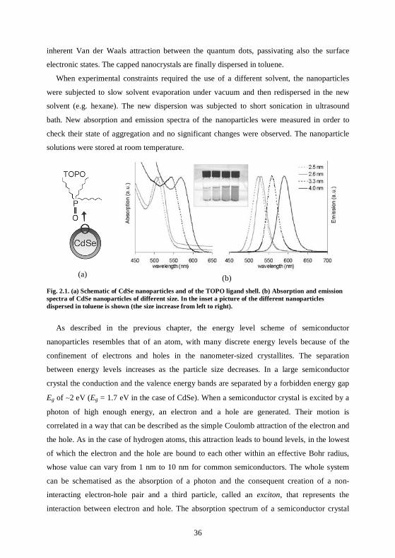
36
inherent Van der Waals attraction between the quantum dots, passivating also the surface
electronic states. The capped nanocrystals are finally dispersed in toluene.
When experimental constraints required the use of a different solvent, the nanoparticles
were subjected to slow solvent evaporation under vacuum and then redispersed in the new
solvent (e.g. hexane). The new dispersion was subjected to short sonication in ultrasound
bath. New absorption and emission spectra of the nanoparticles were measured in order to
check their state of aggregation and no significant changes were observed. The nanoparticle
solutions were stored at room temperature.
(a) (b)
Fig. 2.1. (a) Schematic of CdSe nanoparticles and of the TOPO ligand shell. (b) Absorption and emission spectra of CdSe nanoparticles of different size. In the inset a picture of the different nanoparticles dispersed in toluene is shown (the size increase from left to right).
As described in the previous chapter, the energy level scheme of semiconductor
nanoparticles resembles that of an atom, with many discrete energy levels because of the
confinement of electrons and holes in the nanometer-sized crystallites. The separation
between energy levels increases as the particle size decreases. In a large semiconductor
crystal the conduction and the valence energy bands are separated by a forbidden energy gap
Eg of ∼2 eV (Eg = 1.7 eV in the case of CdSe). When a semiconductor crystal is excited by a
photon of high enough energy, an electron and a hole are generated. Their motion is
correlated in a way that can be described as the simple Coulomb attraction of the electron and
the hole. As in the case of hydrogen atoms, this attraction leads to bound levels, in the lowest
of which the electron and the hole are bound to each other within an effective Bohr radius,
whose value can vary from 1 nm to 10 nm for common semiconductors. The whole system
can be schematised as the absorption of a photon and the consequent creation of a non-
interacting electron-hole pair and a third particle, called an exciton, that represents the
interaction between electron and hole. The absorption spectrum of a semiconductor crystal
37
exhibits a pronounced resonance peak at the energy Eg-Ry, where Ry is the Rydberg energy
which is inversely proportional to the Bohr radius. As the size of the crystal approaches that
of its Bohr radius, the energy gap Eg increases and splits into discrete energy levels because of
the spatial confinement [101]. Consequently, the absorption and the emission of
semiconductor crystals are generally shifted to wavelengths in the visible and in the
ultraviolet.
Fig. 2.1b shows the normalized absorption and emission spectra of CdSe nanoparticles in
toluene ranging from 2.5 nm to 4.0 nm in diameter, where the size of the nanoparticles was
estimated from the position of the first absorption maximum (exciton peak) [102]. A decrease
in size corresponds to a blue shift of both spectra. The inset is a picture of the four particle
samples, whose colours range from yellow to red with the increase in the diameter of the
particles. The narrow emission spectra are an indication of the good monodispersity of the
particles (better than 10%).
Phenomena such as the turning on and off of the fluorescence (blinking), the stopping of
the fluorescence (bleaching) and the dependency of the fluorescence intensity on the
polarization of the excitation beam are typical behaviour of single crystal [103;104;105].
The blinking mechanism for semiconductor nanoparticles has not been yet fully
understood [103;106]. It is found that the average on time is about inversely proportional to
the excitation intensity, while the average off time is intensity independent. This supports the
hypothesis that blinking is a light-induced process, while the off times are determined by the
spontaneous lifetime of the non-fluorescent state. At the moment, the explanation that finds
more experimental support presupposes that blinking involves electron or hole tunnelling
events that photoionize the quantum dot. Both on time and off time probability density studies
suggest multiple ionisation states and consequently a distribution of recombination rates
[103].
Bleaching events are probably due to photo-oxidation of the nanocrystal surface [107;105].
It is found that single quantum dot emission undergoes a blue-shift under constant irradiation
in air that can be explained by a shrinking of the crystal due to the oxidation of the outer
atoms shell (or shells). As a result of photo-oxidation at the surface, quenching states are
formed at the CdSe/CdSe oxide interface that decrease the number of photons emitted until
the particle does not emit anymore. This model is supported by the fact that bleaching is
found to be slower when nanoparticles are in a nitrogen atmosphere, or if they are capped
with a thick inorganic shell [107].
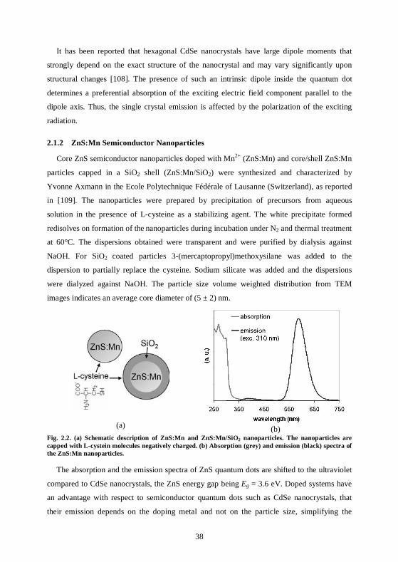
38
It has been reported that hexagonal CdSe nanocrystals have large dipole moments that
strongly depend on the exact structure of the nanocrystal and may vary significantly upon
structural changes [108]. The presence of such an intrinsic dipole inside the quantum dot
determines a preferential absorption of the exciting electric field component parallel to the
dipole axis. Thus, the single crystal emission is affected by the polarization of the exciting
radiation.
2.1.2 ZnS:Mn Semiconductor Nanoparticles
Core ZnS semiconductor nanoparticles doped with Mn2+ (ZnS:Mn) and core/shell ZnS:Mn
particles capped in a SiO2 shell (ZnS:Mn/SiO2) were synthesized and characterized by
Yvonne Axmann in the Ecole Polytechnique Fédérale of Lausanne (Switzerland), as reported
in [109]. The nanoparticles were prepared by precipitation of precursors from aqueous
solution in the presence of L-cysteine as a stabilizing agent. The white precipitate formed
redisolves on formation of the nanoparticles during incubation under N2 and thermal treatment
at 60°C. The dispersions obtained were transparent and were purified by dialysis against
NaOH. For SiO2 coated particles 3-(mercaptopropyl)methoxysilane was added to the
dispersion to partially replace the cysteine. Sodium silicate was added and the dispersions
were dialyzed against NaOH. The particle size volume weighted distribution from TEM
images indicates an average core diameter of (5 ± 2) nm.
(a) (b)
Fig. 2.2. (a) Schematic description of ZnS:Mn and ZnS:Mn/SiO2 nanoparticles. The nanoparticles are capped with L-cystein molecules negatively charged. (b) Absorption (grey) and emission (black) spectra of the ZnS:Mn nanoparticles.
The absorption and the emission spectra of ZnS quantum dots are shifted to the ultraviolet
compared to CdSe nanocrystals, the ZnS energy gap being Eg = 3.6 eV. Doped systems have
an advantage with respect to semiconductor quantum dots such as CdSe nanocrystals, that
their emission depends on the doping metal and not on the particle size, simplifying the
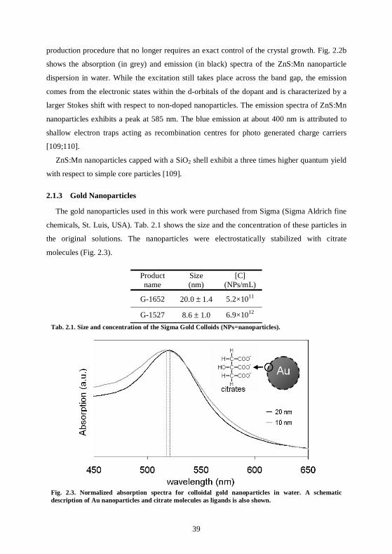
39
production procedure that no longer requires an exact control of the crystal growth. Fig. 2.2b
shows the absorption (in grey) and emission (in black) spectra of the ZnS:Mn nanoparticle
dispersion in water. While the excitation still takes place across the band gap, the emission
comes from the electronic states within the d-orbitals of the dopant and is characterized by a
larger Stokes shift with respect to non-doped nanoparticles. The emission spectra of ZnS:Mn
nanoparticles exhibits a peak at 585 nm. The blue emission at about 400 nm is attributed to
shallow electron traps acting as recombination centres for photo generated charge carriers
[109;110].
ZnS:Mn nanoparticles capped with a SiO2 shell exhibit a three times higher quantum yield
with respect to simple core particles [109].
2.1.3 Gold Nanoparticles
The gold nanoparticles used in this work were purchased from Sigma (Sigma Aldrich fine
chemicals, St. Luis, USA). Tab. 2.1 shows the size and the concentration of these particles in
the original solutions. The nanoparticles were electrostatically stabilized with citrate
molecules (Fig. 2.3).
Product name
Size (nm)
[C] (NPs/mL)
G-1652 20.0 ± 1.4 5.2×10¹¹
G-1527 8.6 ± 1.0 6.9×10¹²
Tab. 2.1. Size and concentration of the Sigma Gold Colloids (NPs=nanoparticles).
Fig. 2.3. Normalized absorption spectra for colloidal gold nanoparticles in water. A schematic description of Au nanoparticles and citrate molecules as ligands is also shown.
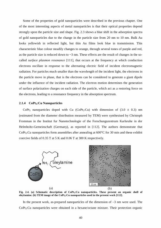
40
Some of the properties of gold nanoparticles were described in the previous chapter. One
of the most interesting aspects of metal nanoparticles is that their optical properties depend
strongly upon the particle size and shape. Fig. 2.3 shows a blue shift in the adsorption spectra
of gold nanoparticles due to the change in the particle size from 20 nm to 10 nm. Bulk Au
looks yellowish in reflected light, but thin Au films look blue in transmission. This
characteristic blue colour steadily changes to orange, through several tones of purple and red,
as the particle size is reduced down to ~3 nm. These effects are the result of changes in the so-
called surface plasmon resonance [111], that occurs at the frequency at which conduction
electrons oscillate in response to the alternating electric field of incident electromagnetic
radiation. For particles much smaller than the wavelength of the incident light, the electrons in
the particle move in phase, that is the electrons can be considered to generate a giant dipole
under the influence of the incident radiation. The electron motion determines the generation
of surface polarization charges on each side of the particle, which act as a restoring force on
the electrons, leading to a resonance frequency in the absorption spectrum.
2.1.4 CoPt3:Cu Nanoparticles
CoPt3 nanoparticles doped with Cu (CoPt3:Cu) with dimension of (3.0 ± 0.3) nm
(estimated from the diameter distribution measured by TEM) were synthesised by Christoph
Fromman in the Institut fur Nanotechnologie of the Forschungszentrum Karlsruhe in der
Helmholtz-Gemeinschaft (Germany), as reported in [112]. The authors demonstrate that
CoPt3:Cu nanoparticles form assemblies after annealing at 600°C for 30 min and these exhibit
coercive fields of 0.35 T at 5 K and 0.06 T at 300 K respectively.
(a)
(b) Fig. 2.4. (a) Schematic description of CoPt3:Cu nanoparticles. These present an organic shell of oleylamine. (b) TEM image of the CoPt3:Cu nanoparticles used in the present work [112].
In the present work, as-prepared nanoparticles of the dimension of ∼3 nm were used. The
CoPt3:Cu nanoparticles were obtained in a hexane/octane mixture. Their protection organic
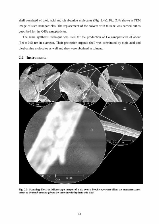
41
shell consisted of oleic acid and oleyl-amine molecules (Fig. 2.4a). Fig. 2.4b shows a TEM
image of such nanoparticles. The replacement of the solvent with toluene was carried out as
described for the CdSe nanoparticles.
The same synthesis technique was used for the production of Co nanoparticles of about
(5.0 ± 0.5) nm in diameter. Their protection organic shell was constituted by oleic acid and
oleyl-amine molecules as well and they were obtained in toluene.
2.2 Instruments
Fig. 2.5. Scanning Electron Microscope images of a tic over a block-copolymer film: the nanostructures result to be much smaller (about 50 times in width) than a tic hair.
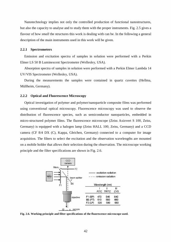
42
Nanotechnology implies not only the controlled production of functional nanostructures,
but also the capacity to analyse and to study them with the proper instruments. Fig. 2.5 gives a
flavour of how small the structures this work is dealing with can be. In the following a general
description of the main instruments used in this work will be given.
2.2.1 Spectrometers
Emission and excitation spectra of samples in solution were performed with a Perkin
Elmer LS 50 B Luminescent Spectrometer (Wellesley, USA).
Absorption spectra of samples in solution were performed with a Perkin Elmer Lambda 14
UV/VIS Spectrometer (Wellesley, USA).
During the measurements the samples were contained in quartz cuvettes (Hellma,
Müllheim, Germany).
2.2.2 Optical and Fluorescence Microscopy
Optical investigation of polymer and polymer/nanoparticle composite films was performed
using conventional optical microscopy. Fluorescence microscopy was used to observe the
distribution of fluorescence species, such as semiconductor nanoparticles, embedded in
micro-structured polymer films. The fluorescence microscope (Zeiss Axiovert S 100, Zeiss,
Germany) is equipped with a halogen lamp (Zeiss HALL 100, Zeiss, Germany) and a CCD
camera (CF 8/4 DX (C), Kappa, Gleichen, Germany) connected to a computer for image
acquisition. The filters to select the excitation and the observation wavelengths are mounted
on a mobile holder that allows their selection during the observation. The microscope working
principle and the filter specifications are shown in Fig. 2.6.
Fig. 2.6. Working principle and filter specifications of the fluorescence microscope used.
43
2.2.3 Confocal Optical Microscopy (CM)
In a conventional wide-field optical microscope, the sample is illuminated fairly uniformly.
Information is obtained in the image plane over the whole field of view of the microscope,
and along the optical axis over the whole sample thickness. A discrimination of depth
information is only attained through contrast, which is highest in the focal plane. Wide-field
microscopy is a fast technique but it is associated with a high background, which can easily
hide small signals. In contrast, CM reduces the background considerably and has an improved
optical resolution.
In CM the image is acquired as a serial process by scanning a confined excitation volume
over the sample and recording the response point by point.
Fig. 2.7a illustrates the confocal principle. The light originating from a point-like source PS
is imaged via a (dichroic) beam splitter onto the object plane by a lens creating a diffraction-
limited spot. There, the light interacts with the object PO. The same lens collects the resulting
optical signal and images it onto a point-like detector PD. Hence, light source, object point and
detector are all conjugated points in the imaging system. Light originating from outside the
focus (for example points A and B in Fig. 2.7b) is not imaged onto the detector and therefore
not detected. Moreover points outside the focus are barely excited. This confinement of the
excitation and detection volume reduces background light efficiently, increases optical
resolution and allows acquisition of three-dimensional images of a thick sample by acquiring
images of several object planes, which are combined afterward by a computer.
Fig. 2.7. Confocal principle. a) The focus is created by imaging a point-like light source PS via the objective lens into the focal plane. Light emerging from the focal volume P0 is collected by the same lens, separated from the source light by a beam splitter BS, imaged onto the detection pinhole PD and detected by detector D. b) Light emerging from out of focus objects like A and B is not imaged onto the detection pinhole PD and is hardly detected.
44
One of the CMs used in the present work is a homemade instrument [113]. The laser light
source is an Ar+-laser (main lines: 488 nm / 100 mW, ION Laser Technology, Utah, USA. A
red HeNe–laser 632.8 nm /5 mW, Polytec, Germany, was used during the alignment
procedures). The beam polarization can be tuned to any state and can be changed between
trace and retrace of the same scanning. The samples are mounted on glass coverslips. The
fluorescence light is collected by the objective lens and filtered by a dichroic beam splitter
reflecting the excitation and transmitting the fluorescence light and a number of emission
filters matching the emission spectra of the nanoparticles under measurement. The spectrally-
cleaned fluorescence light is split by a polarizing cube beam splitter (Newport, USA) into two
perpendicularly polarised beams. Finally the fluorescence light in each of the two beams is
focused by a lens onto the core of a multi-mode fibre connected to a single photon counting
avalanche photodiodes (EG&G, Canada). Therefore, four images can be obtained for every
scan, depending on the polarization of the excitation beam and on the detected polarization of
the light emitted by the nanoparticles.
The second CM used during this work (WITec, Germany) is equipped with a frequency
doubled Nd:YAG laser (meanline 532 nm). This was used in a simplified configuration, with
one tunable polarization of the excitation beam and one detection channel.
2.2.4 Atomic Force Microscopy (AFM)
The AFMs [114] used in the present work are a Scanning Probe Microscope (Dimension
3100, Veeco Digital Instruments, New York, USA) equipped with a NanoScope IIIa
controller (Veeco, New York, USA) and a Multimode Scanning Probe Microscope (Veeco
Digital Instruments, New York, USA) equipped with a NanoScope IV controller (Veeco, New
York, USA). They are based on the beam-bounce system [115] consisting of an optical beam
reflected from the mirrored surface on the back side of the cantilever onto a position-sensitive
photodetector. In this arrangement a small deflection of the cantilever will tilt the reflected
beam and change the position of beam on the photodetector. A sharp tip extended down from
the end of a cantilever is scanned relative to the sample and a feedback mechanism enables
the piezo-electric scanners to maintain the tip at a constant force (to obtain height
information), or height (to obtain force information) above the sample surface. As the tip
scans the surface of the sample, moving up and down with the profile of the surface, the laser
beam is deflected off the attached cantilever into a four element photodiode. The
photodetector measures the difference in light intensities between the upper and lower
photodetectors, and converts the signal into a voltage.

45
Fig. 2.8. AFM working principle.
Many AFM modes have been developed for special purposes while the technique of AFM
was becoming mature. Here only the commonly used modes are described.
In contact mode the tip scans the sample in close contact with the surface. The force on the
tip is in the nano-newton range and it is set by pushing the cantilever against the sample
surface with a piezoelectric positioning element. The deflection of the cantilever is sensed and
compared in a DC feedback amplifier to some desired value of deflection; if the measured
deflection is different from the desired value, the feedback amplifier applies a voltage to the
piezo to raise or lower the sample relative to the cantilever to restore the desired value of
deflection. The voltage that the feedback amplifier applies to the piezo is a measure of the
height of the features on the sample surface, which is displayed as a function of the lateral
position of the sample.
Excessive forces applied by the probe to the sample can cause problems such as, for
example, sample damage and tip damage. Minimizing the contact force can reduce these
effects, but there are practical limits to the magnitude of the force that can be controlled by
the user during operation in ambient environments. In addition, phenomena such as the
adsorption of a water vapour and nitrogen monolayer on the sample and tip surfaces and
electrostatic interactions between the sample and the tip can contribute to additional attractive
forces between the probe and sample. All of these effects combine, creating a substantial
frictional force as the probe scans over the sample. In practice, it appears that these frictional
forces are far more destructive than the normal force and can damage the sample, dull the
cantilever probe and distort the resulting data.
The frictional forces between the tip and the sample can be detected when the cantilever is
moving in the direction perpendicular to its main axis (friction mode). The forces cause
torsion of the cantilever during the scanning, which can be measured by the difference in
46
signal between the left and the right photodetectors. Friction and topographical images can be
acquired at the same time during the scanning. This mode can be used to detect variations in
the surface energy of a sample, but does not provide quantitative measurements of it.
Tapping mode is a key advance in AFM. This powerful technique allows high-resolution
topographic imaging of sample surfaces that are easily damaged, loosely bound to their
substrate, or difficult to image by other AFM techniques. It consists in alternately placing the
tip in contact with the surface and then lifting the tip off the surface to avoid dragging the tip
across the surface. The cantilever oscillates near the cantilever's resonant frequency using a
piezoelectric crystal. The oscillating tip is moved toward the surface until it begins to lightly
touch it and then it follows the surface profile continuing the oscillations. When the tip passes
over a bump in the surface, the cantilever has less space to oscillate and the amplitude of
oscillation decreases; conversely, when the tip passes over a depression, the cantilever has
more space to oscillate and the amplitude increases (approaching the maximum free air
amplitude). A digital feedback loop then adjusts the tip-sample separation to maintain
constant amplitude and force on the sample. Unlike contact mode, the tapping mode presents
the advantage that when the tip contacts the surface, it has sufficient oscillation amplitude to
overcome the tip-sample adhesion forces. Also, the surface material is not pulled sideways by
shear forces since the applied force is always vertical.
Phase imaging is a powerful extension of tapping mode that provides information about
surface structure by mapping the phase of the cantilever oscillation during the scan. Together
with the topography of the sample, variations in composition, adhesion and elasticity can be
detected. Applications include identification of contaminants, mapping of different
components in composite materials, and differentiating regions of high and low surface
adhesion or hardness.
2.2.5 Electron Microscopy
Light microscopes are widely used for imaging due to their relative ease of use. However,
their maximum resolution is determined by the wavelength of the photons that are used to
probe the sample. Since electrons have both wave and particle properties, a beam of electrons
can in some circumstances be made to behave like a beam of radiation. The wavelength is
dependent on the electron energy and can be much smaller than that of light. Nevertheless
they can still interact with the sample due to their electrical charge. Light microscopes allow a
resolution of about 0.2 µm, whereas electron microscopes can have resolutions as low as
0.1 nm.
47
Electron microscopes [116] make use of high voltage electron beams generated by
thermoionic or field emission that are focused by magnetic lenses on the specimen. They are
then magnified by a series of magnetic lenses until they hit a photographic plate or light
sensitive sensors producing the so-called electron micrograph. The Transmission Electron
Microscope (TEM) produces images by detecting electrons that are transmitted through the
sample, while the Scanning Electron Microscope (SEM) produces images by detecting
secondary electrons which are emitted from the surface due to excitation by the primary
electron beam. Generally, TEM resolution is about an order of magnitude better than SEM
resolution. However, since the SEM image relies on surface processes rather than
transmission, it can produce characteristic 3-dimensional quality images, useful for judging
the surface structure of the sample.
The SEM used in this work is a Philips ESEM-FEG XL30 (Philips, Netherlands), equipped
with an Energy Dispersive X-ray Spectroscopy (EDAX, Mahwah, USA) for chemical
analysis. The electron beam has an energy ranging from a 200 V to 30 keV. As the primary
electrons strike the surface they are elastically and inelastically scattered by atoms in the
sample. Through these scattering events, the primary beam effectively spreads inside a sample
volume and the interactions in this region lead to the subsequent emission of secondary
electrons, back scattered electrons and characteristic X-Ray. By using the appropriate
detectors, images or chemical analyses are obtained. The standard imaging mode consists of
the detection of secondary electrons; due to their low energy, these electrons must originate
from within a few tenths of a nanometer from the surface. The brightness of the signal
depends on the surface area exposed to the primary beam that is relatively small for a flat
surface, but increases for steep surfaces. Thus steep surface and edges tend to be brighter than
flat surfaces, giving images with good three-dimensional contrast. Using this technique,
resolutions on the order of 2 nm are possible.
The TEM (CM 200, Philips, Netherlands equipped with Energy Dispersive X-ray
Spectroscopy, EDAX, Mahwah, USA for chemical analysis) was used for high resolution
images of the nanoparticles embedded in a polymer film.
2.3 Solvents
In this work the solvents had different roles: not only they were used to dissolve polymeric
molecules or nanoparticles, but they also had an active role in the experiments to promote
specific adsorption behaviour of the nanoparticles to different polymer surfaces.
48
The use of techniques based on nanoparticle fluorescence detection required the reduction
of sources of sample contamination, as for example the presence of organic molecules in the
solvents. Moreover, the substrate surface energy turned out to be a critical parameter for the
experiment, requiring strict protocols for their cleaning and solvents of an appropriate quality.
Thus, a careful choice of the solvent quality and its handling were fundamental for the
reproducibility and the cleanness of the experiments. In Tab. 2.2 the main solvents used in
this work and the relative use is described.
Solvent Quality Production company Use
Water MilliQ Millipore, Billerica,
USA
Washing, rinsing, polymer and
nanoparticle solvent Chloroform for spectroscopy Polymer solvent.
Hexane for spectroscopy Nanoparticle solvent.
Cyclohexane puriss for analysis Polymer removal
Acetone for spectroscopy Substrate pre-
washing
Methanol for spectroscopy Polymer solvent
Ethanol (high quality)
for spectroscopy
Merck, Merck & Co. Whitehouse Station,
USA
Thiol solvent, polymer removal
Ethanol (low quality)
puriss for analysis Substrate pre-
washing
Toluene for spectroscopy
Fluka, Sigma Aldrich fine chemicals, St. Luis,
USA Polymer and
nanoparticle solvent
MEK for spectroscopy Sigma Aldrich fine chemicals, St. Luis,
USA Polymer solvent
Acetic Acid 99.8% VLSI Polymer removal
Sulphuric acid 96% VLSI Piranha solution
Hydrogen peroxide 30%
VLSI Piranha solution and
SC-1 solution Ammonia 28% VLSI
Rockwood Electronic Materials, Rockwood
Speciality Group, Princeton, USA
SC-1 solution
Tab. 2.2. Description of the solvents used in this work and of their use.
2.4 Oxygen plasma
Oxygen plasma processes were performed with an Oxford Instruments Plasmalab 80 Plus
(Oxford Instruments Plasma Technology, Bristol, United Kingdom, equipped with an Astex

49
AX2107 Microwave Power Generator, Applied Science and Technology, Woburn, USA and a
ENI ACG-3LP4 RF Power Generator, MKS, Wilmington, USA).
Two different kinds of plasma processes were used depending on the application and they
are summarized in Tab. 2.3. A µ-wave oxygen plasma was used for surface cleaning. Radio-
frequency (RF) oxygen plasma was used for polymer etching. The duration of the process
depended on the thickness of the polymer layer to be removed and usually ranged between
3 min and 10 min. This process was also used to remove the protective organic shell of gold
nanoparticles.
Function Gas Gas
pressure (Torr)
Holder temperature
(K)
Generator type
Generator Power (W)
Time
Surface cleaning
O2 0.250 273 µ-wave 250 3 min
- - 20 s +
Polymer etching
O2 0.050 283
RF 30 3÷10 min
Tab. 2.3. Summary of the plasma processes used and their function.
2.5 Substrate preparation
The samples were prepared on different substrates, depending on the experimental
requirements.
Glass coverslips (170 µm thick, Menzel, Germany) were cleaned by sonication for 30
minutes at 35°C in a 2 % solution of Hellmanex (Hellma, Müllheim, Germany) in milliQ
water, and washed in deionised water (3 times 5 minutes with sonication).
Silicon slides (<100>, Siltronix, Archamps, France) were cleaned with the following
procedure:
• Pre-washing: 5 minutes sonication of the slides in a solution of acetone:ethanol
50:50. Rinsing in MilliQ water.
• Removal of organic residues: 10 minutes in piranha solution (sulphuric
acid:hydrogen peroxide 4:1) at 120°C. Abundant rinsing in flowing MilliQ water.
• Removal of metal residues: 10 minutes in SC-1 solution (water:ammonia:hydrogen
peroxide 5:1:1) at 70°C. Abundant rinsing in flowing MilliQ water.
The freshly cleaned silicon substrates were highly hydrophilic (advancing water contact
angle below 5°). The substrate surface could be silanized to vary its surface energy.
50
Gold and chromium surfaces were produced by thermal evaporation (AUTO 306
Evaporation System, BOC Edwards, United Kingdom) onto a cleaned glass or silicon
substrate. Gold films were formed over a few nanometers of chromium. Approximately
40 nm thick gold films were sufficiently transparent to allow bright-field optical
measurements when required. To avoid contamination, the samples were deposited on the
metal surfaces immediately after evaporation. Gold surfaces were covered by thiol
monolayers to obtain substrates with different surface energies; the freshly evaporated gold
surfaces were dipped for one minute in a solution of ethanol containing hexadecanethiol
(CH3(CH2)15SH, Lancaster Synthesis, United Kingdom), mercaptohexadecanoic acid
(COOH(CH2)15SH, Aldrich, Sigma Aldrich fine chemicals, St. Luis, USA) or a mixture of the
two (typical concentrations: from 0.5 mM to 1 mM), rinsed in ethanol and dried with
nitrogen. CH3(CH2)15SH confers an hydrophobic character to the gold surface, while the
COOH(CH2)15SH an hydrophilic one; using a mixture of the two an intermediate wettability
could be achieved.
2.5.1 Micro-contact printing
Micro-contact printing [35] was used to create lateral variations in surface energy. Two
silicon masters were used to make the poly(dimethylsiloxane) (PDMS, Sylgard 184) stamps.
One was produced by IBM (Zurich, CH) and had photoresist structures on the surface. The
structures that were used in the present work were 10 µm wide parallel lines separated by
10 µm wide and 1 µm deep grooves (periodicity 20 µm), and 1 µm wide parallel lines
separated by 1 µm wide and 1 µm deep grooves (periodicity 2 µm). The second stamp was in
silicon and was fabricated by IMT (Neuchâtel, CH). It had several different surface structures.
We used a structure made of parallel lines separated by 3 µm deep grooves; the width of the
lines and of the grooves varied along the structure so that the total width of a consecutive line
and groove was always 8 µm. The narrowest line was 1 µm wide and the widest 7 µm wide.
Before use, the master was silanized with 1H-1H-2H-2H-perfluorodecyltrichlorosilane (A
Better Choice for Research chemicals, Karlsruhe, Germany).
The PDMS stamp was prepared according to the manufacturer’s directions, by mixing 1
part catalyst with 10 parts base resin. The two components were mixed under continuous
stirring for 10 minutes and placed in a vacuum desiccator for 1 hour in order to eliminate air
bubbles from the mixture. The silicon master was placed on a large plastic Petri dish and a
teflon ring was fitted around the edges of the wafer to contain the PDMS. The pre-polymer
was poured onto the wafer and annealed for about 20 hours at 80°C. The PDMS stamp and
51
the master were turned upside down during the last two hours of annealing. After the PDMS
stamp was peeled off from the master, AFM and optical investigation generally revealed good
transfer of topography to the PDMS stamp and no PDMS left on the master. The master was
left for 10 minutes in hexane for cleaning, rinsed with hexane and dried under nitrogen. After
cleaning, the masters were immediately covered with a freshly prepared PDMS pre-polymer
in order to avoid surface contamination, and the stamp was annealed as described before. If
the PDMS stamp was not required immediately, the master was stored without its removal.
The resulting PDMS stamps were 4 mm thick and were cut into small stamps
approximately 0.25 cm2. They were stored in plastic pillboxes taking care that the structured
sides were always in contact with the box surface in order to avoid air contamination. The
same PDMS stamp was used several times but always with the same organic molecules.
Before use they were cleaned with ethanol in an ultrasound bath for some minutes and dried
with nitrogen.
(a)
(b)
(c)
(d) Fig. 2.9. (a) Scheme of the micro-contact printing technique procedure. (b) Schematic representation of the gold surface functionalised with hexadecanethiol and mercaptohexadecanoic acid. (c) AFM topography and (d) AFM friction image of a gold substrate patterned by micro contact printing with alternating stripes of hexadecanethiol and mercaptohexadecanoic acid.
The patterns realized by micro-contact printing consisted of monolayers of different kinds
of thiols on gold surfaces [117]. Fig. 2.9a shows a schematic of the procedure used: a PDMS
stamp was inked with CH3(CH2)15SH, 1 mM in ethanol for 1 min and placed in contact with
the freshly evaporated gold surface for 10 s. An initial contact occurs locally at protrusions of
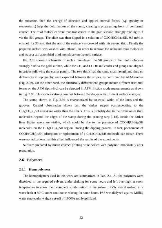
52
the substrate, then the energy of adhesion and applied normal forces (e.g. gravity or
electrostatic) help the deformation of the stamp, creating a propagating front of conformal
contact. The thiol molecules were thus transferred to the gold surface, strongly binding to it
via the SH groups. The slide was then dipped in a solution of COOH(CH2)15SH, 0.5 mM in
ethanol, for 30 s, so that the rest of the surface was covered with this second thiol. Finally the
prepared surface was washed with ethanol, in order to remove the unbound thiol molecules
and leave a self assembled thiol monolayer on the gold surface.
Fig. 2.9b shows a schematic of such a monolayer: the SH groups of the thiol molecules
strongly bind to the gold surface, while the CH3 and COOH molecular end groups are aligned
in stripes following the stamp pattern. The two thiols had the same chain length and thus no
differences in topography were expected between the stripes, as confirmed by AFM studies
(Fig. 2.9c). On the other hand, the chemically different end groups induce different frictional
forces on the AFM tip, which can be detected in AFM friction mode measurements as shown
in Fig. 2.9d. This shows a strong contrast between the stripes with different surface energies.
The stamp shown in Fig. 2.9d is characterized by an equal width of the lines and the
grooves. Careful observation shows that the darker stripes (corresponding to the
CH3(CH2)15SH areas) are wider than the others. This is probably due to the diffusion of thiol
molecules beyond the edges of the stamp during the printing step [118]. Inside the darker
lines lighter spots are visible, which could be due to the presence of COOH(CH2)15SH
molecules on the CH3(CH2)15SH region. During the dipping process, in fact, phenomena of
COOH(CH2)15SH adsorption or replacement of a CH3(CH2)15SH molecule can occur. There
were no indications that this effect influenced the results of the experiments.
Surfaces prepared by micro contact printing were coated with polymer immediately after
preparation.
2.6 Polymers
2.6.1 Homopolymers
The homopolymers used in this work are summarized in Tab. 2.4. All the polymers were
dissolved in the required solvent under shaking for some hours and left overnight at room
temperature to allow their complete solubilisation in the solvent. PVA was dissolved in a
water bath at 80°C under continuous stirring for some hours. PSS was dialyzed against MilliQ
water (molecular weight cut-off of 10000) and lyophilized.

53
Fig. 2.10. Spin-coating procedure for the coating of substrates with a polymer film.
Name Abbr. Solvents used
Source Mw Mw/Mn
Poly(styrene) 1890 1.06 10300 1.03
101000 1.03
141000 1.03
226000 1.06
PS
toluene cyclohexane chloroform
Polymer standard service, Mainz,
Germany (PSS)
546000 1.02
PSS and 106000 1.05 Poly(methylmethacrylate)
PMMA toluene
acetic acid
Sigma, Sigma Aldrich fine
chemicals, St. Luis, USA
102600 2.12
Poly(2-vinylpyridine)
P2VP chloroform
ethanol PSS 79100 1.05
Poly(vinylalcohol)
PVA water PSS 40500 1.94
Poly(diallyldimethyl ammonium chloride)
Poly DADMAC
water, acetic acid
PSS 44800 1.47
Poly(ethyleneimine)
PEI water +
0.5M NaCl Sigma 750000 12.5
Poly(sodium 4-styrenesulfonate)
PSS water +
0.5M NaCl
Aldrich, Sigma Aldrich fine chemicals, St. Luis, USA
∼70000
Tab. 2.4. Description of the homopolymers used in this work
54
Polymer 1 Polymer 2 Common solvent
Selective solvent 1
Selective solvent 2
Concentration (w/v)
PS PMMA toluene cyclohexane acetic acid 1 %-3 %
PS P2VP chloroform cyclohexane ethanol 1 %
PVA PolyDADMAC water acetic acid 5 %
Tab. 2.5. Pairs of immiscible polymers with relative common and selective solvents and typical concentrations used.
All the polymer solutions were stored in the fridge to avoid solvent evaporation, but before
the use they were always allowed to equilibrate to room temperature.
The pairs of immiscible polymers used to create structured films by polymer demixing are
shown in Tab. 2.5, together with their common solvent, their selective solvents and the
concentrations typically used. Once the solutions of each polymer were ready, they were
mixed together in the desired ratios and left to mix under shaking for some minutes.
The polymer films were prepared by spin-coating. A drop of solution was deposited on the
clean substrate, the sample holder rotation was started causing the solution to be largely
thrown off the sample and the solvent to evaporate. During the solvent evaporation, the
polymer concentration increases to a threshold value, above which demixing into two phases
takes place. On continued evaporation of the solvent, the polymer film solidifies, ‘freezing in’
the non-equilibrium microphase structure (Fig. 2.10). For the removal of one of the polymer
phases the sample was immersed for 5 minutes in a selective solvent bath and dried under
nitrogen.
The resulting structure is strongly influenced by both the solution characteristics and the
experimental conditions:
• choice of polymers;
• polymer molecular weight;
• common solvent;
• total polymer concentration;
• relative polymer concentration;
• rotation speed;
• substrate surface energy.
PS/PMMA films made by polymer demixing have been extensively characterized
[25;119]. Fig. 2.11a and b show topographic AFM images of a typical PS/PMMA film made
by spin-coating on a clean (hydrophilic) SiO2 surface, before and after removal of PS by
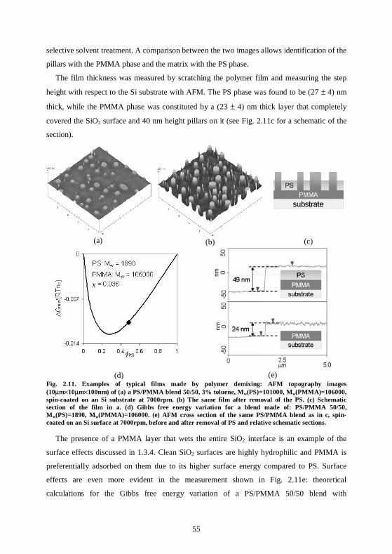
55
selective solvent treatment. A comparison between the two images allows identification of the
pillars with the PMMA phase and the matrix with the PS phase.
The film thickness was measured by scratching the polymer film and measuring the step
height with respect to the Si substrate with AFM. The PS phase was found to be (27 ± 4) nm
thick, while the PMMA phase was constituted by a (23 ± 4) nm thick layer that completely
covered the SiO2 surface and 40 nm height pillars on it (see Fig. 2.11c for a schematic of the
section).
(a)
(b)
(c)
(d)
(e) Fig. 2.11. Examples of typical films made by polymer demixing: AFM topography images (10µm×10µm×100nm) of (a) a PS/PMMA blend 50/50, 3% toluene, Mw(PS)=101000, Mw(PMMA)=106000, spin-coated on an Si substrate at 7000rpm. (b) The same film after removal of the PS. (c) Schematic section of the film in a. (d) Gibbs free energy variation for a blend made of: PS/PMMA 50/50, Mw(PS)=1890, Mw(PMMA)=106000. (e) AFM cross section of the same PS/PMMA blend as in c, spin-coated on an Si surface at 7000rpm, before and after removal of PS and relative schematic sections.
The presence of a PMMA layer that wets the entire SiO2 interface is an example of the
surface effects discussed in 1.3.4. Clean SiO2 surfaces are highly hydrophilic and PMMA is
preferentially adsorbed on them due to its higher surface energy compared to PS. Surface
effects are even more evident in the measurement shown in Fig. 2.11e: theoretical
calculations for the Gibbs free energy variation of a PS/PMMA 50/50 blend with
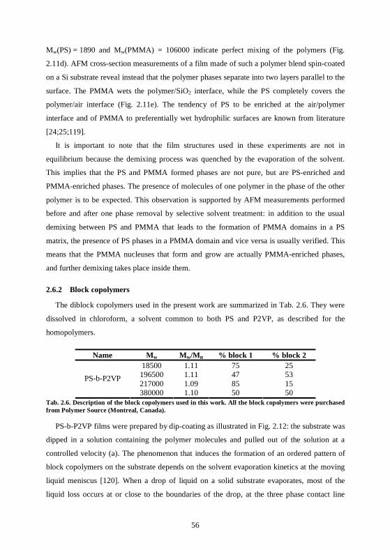
56
Mw(PS) = 1890 and Mw(PMMA) = 106000 indicate perfect mixing of the polymers (Fig.
2.11d). AFM cross-section measurements of a film made of such a polymer blend spin-coated
on a Si substrate reveal instead that the polymer phases separate into two layers parallel to the
surface. The PMMA wets the polymer/SiO2 interface, while the PS completely covers the
polymer/air interface (Fig. 2.11e). The tendency of PS to be enriched at the air/polymer
interface and of PMMA to preferentially wet hydrophilic surfaces are known from literature
[24;25;119].
It is important to note that the film structures used in these experiments are not in
equilibrium because the demixing process was quenched by the evaporation of the solvent.
This implies that the PS and PMMA formed phases are not pure, but are PS-enriched and
PMMA-enriched phases. The presence of molecules of one polymer in the phase of the other
polymer is to be expected. This observation is supported by AFM measurements performed
before and after one phase removal by selective solvent treatment: in addition to the usual
demixing between PS and PMMA that leads to the formation of PMMA domains in a PS
matrix, the presence of PS phases in a PMMA domain and vice versa is usually verified. This
means that the PMMA nucleuses that form and grow are actually PMMA-enriched phases,
and further demixing takes place inside them.
2.6.2 Block copolymers
The diblock copolymers used in the present work are summarized in Tab. 2.6. They were
dissolved in chloroform, a solvent common to both PS and P2VP, as described for the
homopolymers.
Name Mw Mw/Mn % block 1 % block 2 18500 1.11 75 25
196500 1.11 47 53 217000 1.09 85 15
PS-b-P2VP
380000 1.10 50 50 Tab. 2.6. Description of the block copolymers used in this work. All the block copolymers were purchased from Polymer Source (Montreal, Canada).
PS-b-P2VP films were prepared by dip-coating as illustrated in Fig. 2.12: the substrate was
dipped in a solution containing the polymer molecules and pulled out of the solution at a
controlled velocity (a). The phenomenon that induces the formation of an ordered pattern of
block copolymers on the substrate depends on the solvent evaporation kinetics at the moving
liquid meniscus [120]. When a drop of liquid on a solid substrate evaporates, most of the
liquid loss occurs at or close to the boundaries of the drop, at the three phase contact line
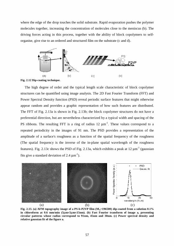
57
where the edge of the drop touches the solid substrate. Rapid evaporation pushes the polymer
molecules together, increasing the concentration of molecules close to the meniscus (b). The
driving forces acting in this process, together with the ability of block copolymers to self-
organise, give rise to an ordered and structured film on the substrate (c and d).
Fig. 2.12 Dip-coating technique.
The high degree of order and the typical length scale characteristic of block copolymer
structures can be quantified using image analysis. The 2D Fast Fourier Transform (FFT) and
Power Spectral Density function (PSD) reveal periodic surface features that might otherwise
appear random and provides a graphic representation of how such features are distributed.
The FFT of Fig. 2.13a is shown in Fig. 2.13b; the block copolymer structures do not have a
preferential direction, but are nevertheless characterized by a typical width and spacing of the
PS ribbons. The resulting FFT is a ring of radius 12 µm-1. These values correspond to a
repeated periodicity in the images of 91 nm. The PSD provides a representation of the
amplitude of a surface's roughness as a function of the spatial frequency of the roughness
(The spatial frequency is the inverse of the in-plane spatial wavelength of the roughness
features). Fig. 2.13c shows the PSD of Fig. 2.13a, which exhibits a peak at 12 µm-1 (gaussian
fits give a standard deviation of 2.4 µm-1).
(a)
(b)
(c)
Fig. 2.13. (a) AFM topography image of a PS-b-P2VP film (Mw=196500) dip-coated from a solution 0.1% in chloroform at 0.6 mm/min (5µm×5µm×15nm). (b) Fast Fourier transform of image a, presenting circular patterns whose radius correspond to 91nm, 45nm and 30nm. (c) Power spectral density and relative gaussian fit of the figure a.

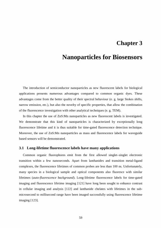
59
Chapter 3
3 Nanoparticles for Biosensors
The introduction of semiconductor nanoparticles as new fluorescent labels for biological
applications presents numerous advantages compared to common organic dyes. These
advantages come from the better quality of their spectral behaviour (e. g. large Stokes shifts,
narrow emission, etc.), but also the novelty of specific properties, that allow the combination
of the fluorescence investigation with other analytical techniques (e. g. TEM).
In this chapter the use of ZnS:Mn nanoparticles as new fluorescent labels is investigated.
We demonstrate that this kind of nanoparticles is characterized by exceptionally long
fluorescence lifetime and it is thus suitable for time-gated fluorescence detection technique.
Moreover, the use of ZnS:Mn nanoparticles as mass and fluorescence labels for waveguide
based sensors will be demonstrated.
3.1 Long-lifetime fluorescence labels have many applications
Common organic fluorophores emit from the first allowed singlet–singlet electronic
transition within a few nanoseconds. Apart from lanthanides and transition metal-ligand
complexes, the fluorescence lifetimes of common probes are less than 100 ns. Unfortunately,
many species in a biological sample and optical components also fluoresce with similar
lifetimes (auto-fluorescence background). Long-lifetime fluorescence labels for time-gated
imaging and fluorescence lifetime imaging [121] have long been sought to enhance contrast
in cellular imaging and analysis [122] and lanthanide chelates with lifetimes in the sub-
microsecond to millisecond range have been imaged successfully using fluorescence lifetime
imaging [123].
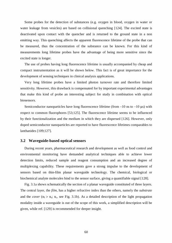
60
Some probes for the detection of substances (e.g. oxygen in blood, oxygen in water or
water leakage from vesicles) are based on collisional quenching [124]. The excited state is
deactivated upon contact with the quencher and is returned to the ground state in a non
emitting way. This quenching affects the apparent fluorescence lifetime of the probe that can
be measured, thus the concentration of the substance can be known. For this kind of
measurements long lifetime probes have the advantage of being more sensitive since the
excited state is longer.
The use of probes having long fluorescence lifetime is usually accompanied by cheap and
compact instrumentation as it will be shown below. This fact is of great importance for the
development of sensing techniques in clinical analysis applications.
Very long lifetime probes have a limited photon turnover rate and therefore limited
sensitivity. However, this drawback is compensated for by important experimental advantages
that make this kind of probe an interesting subject for study in combination with optical
biosensors.
Semiconductor nanoparticles have long fluorescence lifetime (from ∼10 ns to ∼10 µs) with
respect to common fluorophores [53;125]. The fluorescence lifetime seems to be influenced
by their functionalization and the medium in which they are dispersed [126]. However, only
doped semiconductor nanoparticles are reported to have fluorescence lifetimes comparables to
lanthanides [109;127].
3.2 Waveguide-based optical sensors
During recent years, pharmaceutical research and development as well as food control and
environmental monitoring have demanded analytical techniques able to achieve lower
detection limits, reduced sample and reagent consumption and an increased degree of
multiplexing capability. These requirements gave a strong impulse to the development of
sensors based on thin-film planar waveguide technology. The chemical, biological or
biochemical analyte molecules bind to the sensor surface, giving a quantifiable signal [128].
Fig. 3.1a shows schematically the section of a planar waveguide constituted of three layers.
The central layer, the film, has a higher refractive index than the others, namely the substrate
and the cover (nf > ns; nc, see Fig. 3.1b). As a detailed description of the light propagation
modality inside a waveguide is out of the scope of this work, a simplified description will be
given, while ref. [129] is recommended for deeper insight.
61
(a)
(b)
(c)
Fig. 3.1. (a) Schematic section of a waveguide. (b) Variation of the refractive index of the waveguide materials through the section. (c) Grating to couple the light into the waveguide film.
Light is coupled into the waveguide film by means of a grating (Fig. 3.1c). Analogously to
what happens in an optical fibre, the light propagates in the film layer through multiple total
internal reflections that give rise to interference effects. Due to their confinement, the optical
waves propagate only in a discrete set of states (modes). One of the fundamental parameters
for the description of the propagating behaviour of the light in a waveguide is the so-called
effective refractive index denoted by N. It can be used to express the phase velocity of a mode
in complete analogy to the phase velocity of a wave propagating in free space
(v(mode) = c/N). Due to the boundary conditions, only a discrete set of values exists for N and
they depend on the waveguide structure, the waveguide mode and its polarization. The
coupling conditions depend on different parameters, including the incident angle of the light
ϑ, its wavelength λ, the grating periodicity Λ and the layer refractive indexes. In the cover
layer an evanescent field is present and extends for some 200 nm from the film/cover
interface. In sensing applications, the cover layer contains the analyte. This interacts with the
waveguide mode when within the evanescent field. Two typical approaches to waveguide
sensing have been developed so far, based on refractometric and fluorescence techniques.
Fig. 3.2 Schematic of a waveguide sensor with different sensing regions (pad): the different analytes are specifically and selectively adsorbed on the respective binding sites. The pad R is the reference: it allows monitoring of changing due to environmental factors such as the temperature.
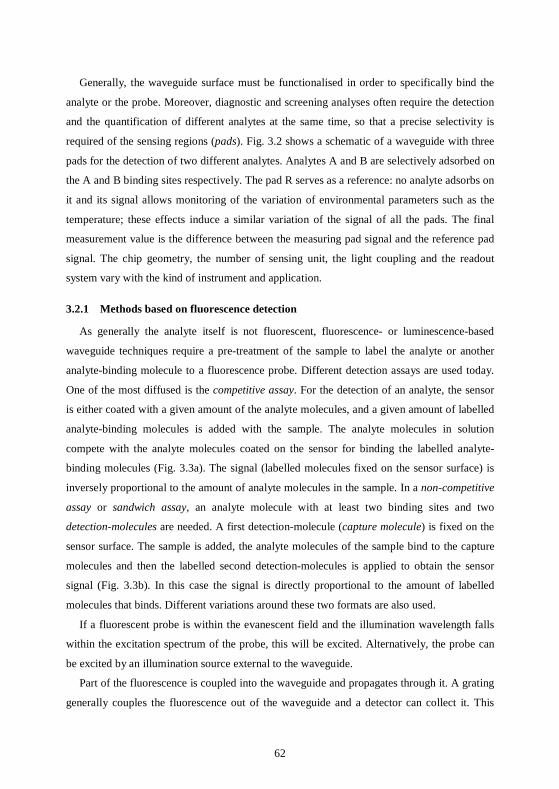
62
Generally, the waveguide surface must be functionalised in order to specifically bind the
analyte or the probe. Moreover, diagnostic and screening analyses often require the detection
and the quantification of different analytes at the same time, so that a precise selectivity is
required of the sensing regions (pads). Fig. 3.2 shows a schematic of a waveguide with three
pads for the detection of two different analytes. Analytes A and B are selectively adsorbed on
the A and B binding sites respectively. The pad R serves as a reference: no analyte adsorbs on
it and its signal allows monitoring of the variation of environmental parameters such as the
temperature; these effects induce a similar variation of the signal of all the pads. The final
measurement value is the difference between the measuring pad signal and the reference pad
signal. The chip geometry, the number of sensing unit, the light coupling and the readout
system vary with the kind of instrument and application.
3.2.1 Methods based on fluorescence detection
As generally the analyte itself is not fluorescent, fluorescence- or luminescence-based
waveguide techniques require a pre-treatment of the sample to label the analyte or another
analyte-binding molecule to a fluorescence probe. Different detection assays are used today.
One of the most diffused is the competitive assay. For the detection of an analyte, the sensor
is either coated with a given amount of the analyte molecules, and a given amount of labelled
analyte-binding molecules is added with the sample. The analyte molecules in solution
compete with the analyte molecules coated on the sensor for binding the labelled analyte-
binding molecules (Fig. 3.3a). The signal (labelled molecules fixed on the sensor surface) is
inversely proportional to the amount of analyte molecules in the sample. In a non-competitive
assay or sandwich assay, an analyte molecule with at least two binding sites and two
detection-molecules are needed. A first detection-molecule (capture molecule) is fixed on the
sensor surface. The sample is added, the analyte molecules of the sample bind to the capture
molecules and then the labelled second detection-molecules is applied to obtain the sensor
signal (Fig. 3.3b). In this case the signal is directly proportional to the amount of labelled
molecules that binds. Different variations around these two formats are also used.
If a fluorescent probe is within the evanescent field and the illumination wavelength falls
within the excitation spectrum of the probe, this will be excited. Alternatively, the probe can
be excited by an illumination source external to the waveguide.
Part of the fluorescence is coupled into the waveguide and propagates through it. A grating
generally couples the fluorescence out of the waveguide and a detector can collect it. This
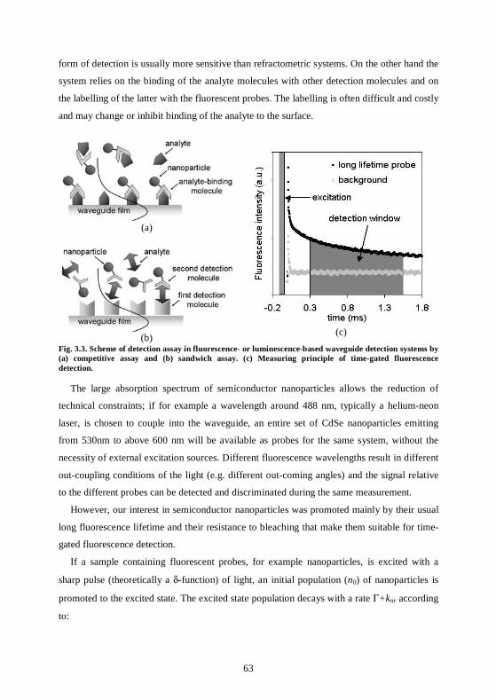
63
form of detection is usually more sensitive than refractometric systems. On the other hand the
system relies on the binding of the analyte molecules with other detection molecules and on
the labelling of the latter with the fluorescent probes. The labelling is often difficult and costly
and may change or inhibit binding of the analyte to the surface.
(a)
(b)
(c)
Fig. 3.3. Scheme of detection assay in fluorescence- or luminescence-based waveguide detection systems by (a) competitive assay and (b) sandwich assay. (c) Measuring principle of time-gated fluorescence detection.
The large absorption spectrum of semiconductor nanoparticles allows the reduction of
technical constraints; if for example a wavelength around 488 nm, typically a helium-neon
laser, is chosen to couple into the waveguide, an entire set of CdSe nanoparticles emitting
from 530nm to above 600 nm will be available as probes for the same system, without the
necessity of external excitation sources. Different fluorescence wavelengths result in different
out-coupling conditions of the light (e.g. different out-coming angles) and the signal relative
to the different probes can be detected and discriminated during the same measurement.
However, our interest in semiconductor nanoparticles was promoted mainly by their usual
long fluorescence lifetime and their resistance to bleaching that make them suitable for time-
gated fluorescence detection.
If a sample containing fluorescent probes, for example nanoparticles, is excited with a
sharp pulse (theoretically a δ-function) of light, an initial population (n0) of nanoparticles is
promoted to the excited state. The excited state population decays with a rate Γ+knr according
to:
64
)()()(
tnkdt
tdnnr+Γ−=
where n(t) is the number of excited nanoparticles at time t following the excitation, Γ is the
emissive rate, and knr is the nonradiative decay rate. Emission is a random event and each
excited nanoparticle has the same probability of emitting in a given period of time. This
results in an exponential decay of the excited state population, ))(exp()( 0 tkntn nr+Γ−= .
During an experiment, what is observed is the fluorescence intensity, which is proportional to
n(t). Writing this decay law in terms of the fluorescence intensity I(t) and integrating it over
the time yields the usual expression for a single exponential decay:
))/(exp()( 0 τtItI −=
where I0 is the intensity at t = 0. The lifetime τ is the inverse of the total decay rate and
corresponds to the mean time a nanoparticle remains in the excited state following the
excitation. The lifetime is a statistical average and the nanoparticles emit randomly
throughout the decay.
The impulse response function I(t) is what would be observed with a δ-function for the
instrument response. Unfortunately, such systems do not exist and many instrument response
functions (response of an instrument to a zero-lifetime sample) are several nanoseconds wide.
The excitation pulse can be represented by a series of δ-functions with different amplitude.
The measured function is thus the sum of different exponential decays starting with different
amplitudes and at different times. However, the discrimination of the fluorescence signal from
the instrument response function is critical only when the two decay lifetimes are comparable.
Fig. 3.3c shows an example of fluorescence gated detection: in black, the fluorescence
emission decay of a long lifetime probe following a pulse excitation, while the background
auto-fluorescence is shown in grey. Biological samples and optical components, as well as
most organic fluorophores, generally exhibit fluorescence decays in the nanosecond range and
the emission is completely gone some hundreds of ns after the excitation pulse. The probe
emission, however, can still be discriminated from the background signal after 1.8 ms. The
long fluorescence lifetime is thus a means to distinguish one or more fluorescent species even
if they emit at similar wavelengths. Moreover, the signal-to-noise ratio is reduced if the
fluorescence signal is integrated over an appropriate time window, for which the background
fluorescence is quasi-zero, but the nanoparticle emission is still high (in grey in the figure).
From the point of view of the instrumentation required, gated detection allows an
improvement of the signal-to-noise ratio and thus of the sensitivity of the instrument.

65
Moreover, it avoids saturation of the detectors by background which can result in a significant
dead time before the signal can be acquired again. Very long lifetime probes in the micro and
millisecond time domain do not require a particularly fast and typically very delicate and
expensive instrumentation.
3.2.2 Methods based on refractometric detection
In refractometric waveguide sensing, the adsorption or the desorption of the analyte
molecules on the waveguide surface gives a variation in the effective refractive index of the
waveguide. This results in a variation of the coupling conditions, for example, the output
angle of the light, that can be detected. This kind of sensor has the advantage of not requiring
labelling of the sample for detection because what is detected is the mass change at the
waveguide surface. The sensitivity of sensors based on label-free analyte detection [130] is
directly related to the molecular mass of the analyte. When low detection limits are required
the sensitivity may not be sufficient. In order to achieve lower detection limits, mass labels
such as latex particles or colloidal gold nanoparticles have been introduced for signal
enhancement [131].
Among the instruments based on refractometric measurements for sensing application
there is the wavelength-interrogated optical sensor (WIOS) [132]. Fig. 3.4 shows a schematic
of the working principle of the WIOS system. The sensor chip is based on a monomode
waveguide structured with two grating regions. The first one acts as in-coupling pad for the
incident beam, and the second grating for coupling the light out of the waveguide onto the
detector. The input grating is illuminated through the transparent substrate with a beam of a
tuneable laser at a fixed angle ϑ1; the wavelength λ(t) of the laser is modulated around
763 nm.
Fig. 3.4. Working principle of WIOS system: the resonance peak of a grating coupler is scanned by means of a current tuneable laser diode. The resonance peak position depends on the effective refractive index of the waveguide [132].
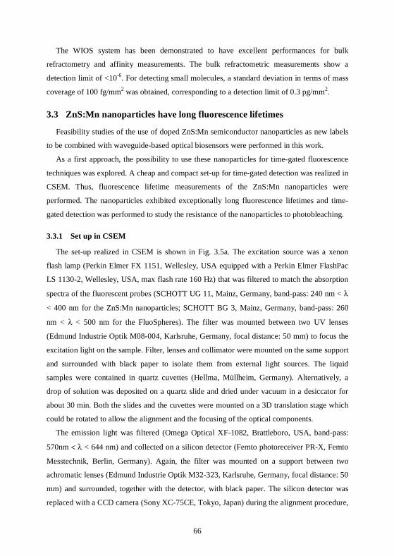
66
The WIOS system has been demonstrated to have excellent performances for bulk
refractometry and affinity measurements. The bulk refractometric measurements show a
detection limit of <10-6. For detecting small molecules, a standard deviation in terms of mass
coverage of 100 fg/mm2 was obtained, corresponding to a detection limit of 0.3 pg/mm2.
3.3 ZnS:Mn nanoparticles have long fluorescence lifetimes
Feasibility studies of the use of doped ZnS:Mn semiconductor nanoparticles as new labels
to be combined with waveguide-based optical biosensors were performed in this work.
As a first approach, the possibility to use these nanoparticles for time-gated fluorescence
techniques was explored. A cheap and compact set-up for time-gated detection was realized in
CSEM. Thus, fluorescence lifetime measurements of the ZnS:Mn nanoparticles were
performed. The nanoparticles exhibited exceptionally long fluorescence lifetimes and time-
gated detection was performed to study the resistance of the nanoparticles to photobleaching.
3.3.1 Set up in CSEM
The set-up realized in CSEM is shown in Fig. 3.5a. The excitation source was a xenon
flash lamp (Perkin Elmer FX 1151, Wellesley, USA equipped with a Perkin Elmer FlashPac
LS 1130-2, Wellesley, USA, max flash rate 160 Hz) that was filtered to match the absorption
spectra of the fluorescent probes (SCHOTT UG 11, Mainz, Germany, band-pass: 240 nm < λ
< 400 nm for the ZnS:Mn nanoparticles; SCHOTT BG 3, Mainz, Germany, band-pass: 260
nm < λ < 500 nm for the FluoSpheres). The filter was mounted between two UV lenses
(Edmund Industrie Optik M08-004, Karlsruhe, Germany, focal distance: 50 mm) to focus the
excitation light on the sample. Filter, lenses and collimator were mounted on the same support
and surrounded with black paper to isolate them from external light sources. The liquid
samples were contained in quartz cuvettes (Hellma, Müllheim, Germany). Alternatively, a
drop of solution was deposited on a quartz slide and dried under vacuum in a desiccator for
about 30 min. Both the slides and the cuvettes were mounted on a 3D translation stage which
could be rotated to allow the alignment and the focusing of the optical components.
The emission light was filtered (Omega Optical XF-1082, Brattleboro, USA, band-pass:
570nm < λ < 644 nm) and collected on a silicon detector (Femto photoreceiver PR-X, Femto
Messtechnik, Berlin, Germany). Again, the filter was mounted on a support between two
achromatic lenses (Edmund Industrie Optik M32-323, Karlsruhe, Germany, focal distance: 50
mm) and surrounded, together with the detector, with black paper. The silicon detector was
replaced with a CCD camera (Sony XC-75CE, Tokyo, Japan) during the alignment procedure,
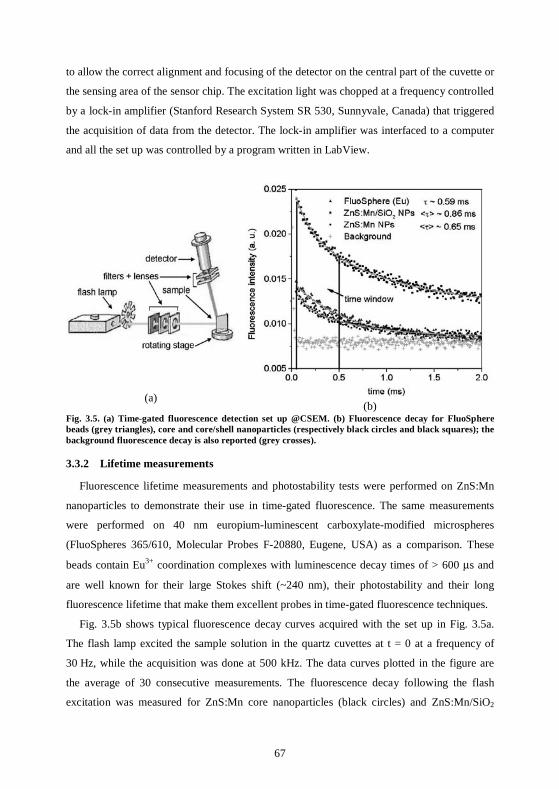
67
to allow the correct alignment and focusing of the detector on the central part of the cuvette or
the sensing area of the sensor chip. The excitation light was chopped at a frequency controlled
by a lock-in amplifier (Stanford Research System SR 530, Sunnyvale, Canada) that triggered
the acquisition of data from the detector. The lock-in amplifier was interfaced to a computer
and all the set up was controlled by a program written in LabView.
(a) (b)
Fig. 3.5. (a) Time-gated fluorescence detection set up @CSEM. (b) Fluorescence decay for FluoSphere beads (grey triangles), core and core/shell nanoparticles (respectively black circles and black squares); the background fluorescence decay is also reported (grey crosses).
3.3.2 Lifetime measurements
Fluorescence lifetime measurements and photostability tests were performed on ZnS:Mn
nanoparticles to demonstrate their use in time-gated fluorescence. The same measurements
were performed on 40 nm europium-luminescent carboxylate-modified microspheres
(FluoSpheres 365/610, Molecular Probes F-20880, Eugene, USA) as a comparison. These
beads contain Eu3+ coordination complexes with luminescence decay times of > 600 µs and
are well known for their large Stokes shift (~240 nm), their photostability and their long
fluorescence lifetime that make them excellent probes in time-gated fluorescence techniques.
Fig. 3.5b shows typical fluorescence decay curves acquired with the set up in Fig. 3.5a.
The flash lamp excited the sample solution in the quartz cuvettes at t = 0 at a frequency of
30 Hz, while the acquisition was done at 500 kHz. The data curves plotted in the figure are
the average of 30 consecutive measurements. The fluorescence decay following the flash
excitation was measured for ZnS:Mn core nanoparticles (black circles) and ZnS:Mn/SiO2
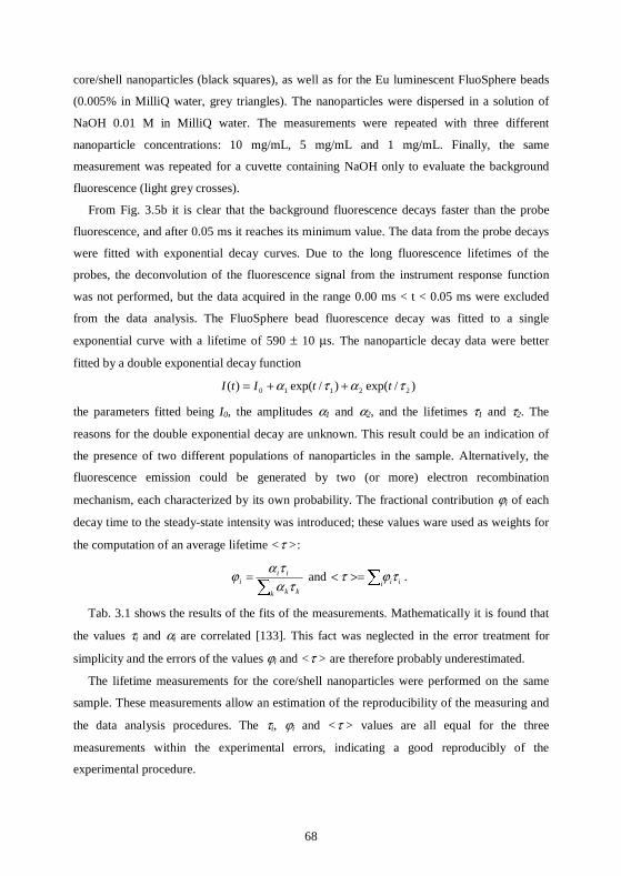
68
core/shell nanoparticles (black squares), as well as for the Eu luminescent FluoSphere beads
(0.005% in MilliQ water, grey triangles). The nanoparticles were dispersed in a solution of
NaOH 0.01 M in MilliQ water. The measurements were repeated with three different
nanoparticle concentrations: 10 mg/mL, 5 mg/mL and 1 mg/mL. Finally, the same
measurement was repeated for a cuvette containing NaOH only to evaluate the background
fluorescence (light grey crosses).
From Fig. 3.5b it is clear that the background fluorescence decays faster than the probe
fluorescence, and after 0.05 ms it reaches its minimum value. The data from the probe decays
were fitted with exponential decay curves. Due to the long fluorescence lifetimes of the
probes, the deconvolution of the fluorescence signal from the instrument response function
was not performed, but the data acquired in the range 0.00 ms < t < 0.05 ms were excluded
from the data analysis. The FluoSphere bead fluorescence decay was fitted to a single
exponential curve with a lifetime of 590 ± 10 µs. The nanoparticle decay data were better
fitted by a double exponential decay function
)/exp()/exp()( 22110 τατα ttItI ++=
the parameters fitted being I0, the amplitudes α1 and α2, and the lifetimes τ1 and τ2. The
reasons for the double exponential decay are unknown. This result could be an indication of
the presence of two different populations of nanoparticles in the sample. Alternatively, the
fluorescence emission could be generated by two (or more) electron recombination
mechanism, each characterized by its own probability. The fractional contribution ϕi of each
decay time to the steady-state intensity was introduced; these values ware used as weights for
the computation of an average lifetime <τ >:
∑=
k kk
iii τα
ταϕ and ∑>=<i iiτϕτ .
Tab. 3.1 shows the results of the fits of the measurements. Mathematically it is found that
the values τi and αi are correlated [133]. This fact was neglected in the error treatment for
simplicity and the errors of the values ϕi and <τ > are therefore probably underestimated.
The lifetime measurements for the core/shell nanoparticles were performed on the same
sample. These measurements allow an estimation of the reproducibility of the measuring and
the data analysis procedures. The τi, ϕi and <τ > values are all equal for the three
measurements within the experimental errors, indicating a good reproducibly of the
experimental procedure.
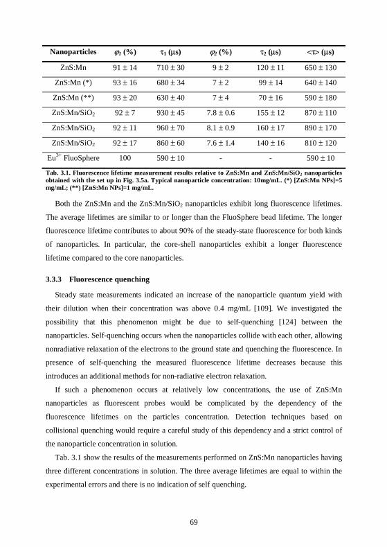
69
Nanoparticles ϕ1 (%) τ1 (µs) ϕ2 (%) τ2 (µs) <τ> (µs)
ZnS:Mn 91 ± 14 710 ± 30 9 ± 2 120 ± 11 650 ± 130
ZnS:Mn (*) 93 ± 16 680 ± 34 7 ± 2 99 ± 14 640 ± 140
ZnS:Mn (**) 93 ± 20 630 ± 40 7 ± 4 70 ± 16 590 ± 180
ZnS:Mn/SiO2 92 ± 7 930 ± 45 7.8 ± 0.6 155 ± 12 870 ± 110
ZnS:Mn/SiO2 92 ± 11 960 ± 70 8.1 ± 0.9 160 ± 17 890 ± 170
ZnS:Mn/SiO2 92 ± 17 860 ± 60 7.6 ± 1.4 140 ± 16 810 ± 120
Eu3+ FluoSphere 100 590 ± 10 - - 590 ± 10
Tab. 3.1. Fluorescence lifetime measurement results relative to ZnS:Mn and ZnS:Mn/SiO2 nanoparticles obtained with the set up in Fig. 3.5a. Typical nanoparticle concentration: 10mg/mL. (*) [ZnS:Mn NPs]=5 mg/mL; (**) [ZnS:Mn NPs]=1 mg/mL.
Both the ZnS:Mn and the ZnS:Mn/SiO2 nanoparticles exhibit long fluorescence lifetimes.
The average lifetimes are similar to or longer than the FluoSphere bead lifetime. The longer
fluorescence lifetime contributes to about 90% of the steady-state fluorescence for both kinds
of nanoparticles. In particular, the core-shell nanoparticles exhibit a longer fluorescence
lifetime compared to the core nanoparticles.
3.3.3 Fluorescence quenching
Steady state measurements indicated an increase of the nanoparticle quantum yield with
their dilution when their concentration was above 0.4 mg/mL [109]. We investigated the
possibility that this phenomenon might be due to self-quenching [124] between the
nanoparticles. Self-quenching occurs when the nanoparticles collide with each other, allowing
nonradiative relaxation of the electrons to the ground state and quenching the fluorescence. In
presence of self-quenching the measured fluorescence lifetime decreases because this
introduces an additional methods for non-radiative electron relaxation.
If such a phenomenon occurs at relatively low concentrations, the use of ZnS:Mn
nanoparticles as fluorescent probes would be complicated by the dependency of the
fluorescence lifetimes on the particles concentration. Detection techniques based on
collisional quenching would require a careful study of this dependency and a strict control of
the nanoparticle concentration in solution.
Tab. 3.1 show the results of the measurements performed on ZnS:Mn nanoparticles having
three different concentrations in solution. The three average lifetimes are equal to within the
experimental errors and there is no indication of self quenching.

70
The measurements described above were performed on samples dispersed in water. The
same measurements were repeated on core nanoparticles deposited on a quartz slide and dried
as described. Here also the long lifetime fluorescence was the major component of the steady-
state fluorescence and had a lifetime of τ1 = (660 ± 120) µs, while the short lifetime was
τ2 = (120 ± 30) µs. The values are averages of three measurements and the errors the maximal
differences among them. As these measurements are in agreement with those performed on
bulk samples, it is concluded that no self quenching is observed for nanoparticle concentration
[C] ≥ 1 mg/mL.
3.3.4 Fluorescence bleaching
The same set up was used to study the fluorescence bleaching of the nanoparticles in
solution. For comparison, identical measurements were performed on the FluoSphere beads.
(a)
(b)
(c)
(d)
Fig. 3.6. Fluorescence bleaching measurement for (a) FluoSpheres beads and (b) ZnS:Mn/SiO2 nanoparticles. (c) The same measurement for the background. (d) Distribution of the measurements in c acquired over 18 min.
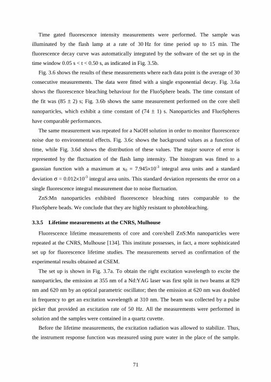
71
Time gated fluorescence intensity measurements were performed. The sample was
illuminated by the flash lamp at a rate of 30 Hz for time period up to 15 min. The
fluorescence decay curve was automatically integrated by the software of the set up in the
time window 0.05 s < t < 0.50 s, as indicated in Fig. 3.5b.
Fig. 3.6 shows the results of these measurements where each data point is the average of 30
consecutive measurements. The data were fitted with a single exponential decay. Fig. 3.6a
shows the fluorescence bleaching behaviour for the FluoSphere beads. The time constant of
the fit was (85 ± 2) s; Fig. 3.6b shows the same measurement performed on the core shell
nanoparticles, which exhibit a time constant of (74 ± 1) s. Nanoparticles and FluoSpheres
have comparable performances.
The same measurement was repeated for a NaOH solution in order to monitor fluorescence
noise due to environmental effects. Fig. 3.6c shows the background values as a function of
time, while Fig. 3.6d shows the distribution of these values. The major source of error is
represented by the fluctuation of the flash lamp intensity. The histogram was fitted to a
gaussian function with a maximum at x0 = 7.945×10⁻³ integral area units and a standard
deviation σ = 0.012×10⁻³ integral area units. This standard deviation represents the error on a
single fluorescence integral measurement due to noise fluctuation.
ZnS:Mn nanoparticles exhibited fluorescence bleaching rates comparable to the
FluoSphere beads. We conclude that they are highly resistant to photobleaching.
3.3.5 Lifetime measurements at the CNRS, Mulhouse
Fluorescence lifetime measurements of core and core/shell ZnS:Mn nanoparticles were
repeated at the CNRS, Mulhouse [134]. This institute possesses, in fact, a more sophisticated
set up for fluorescence lifetime studies. The measurements served as confirmation of the
experimental results obtained at CSEM.
The set up is shown in Fig. 3.7a. To obtain the right excitation wavelength to excite the
nanoparticles, the emission at 355 nm of a Nd:YAG laser was first split in two beams at 829
nm and 620 nm by an optical parametric oscillator; then the emission at 620 nm was doubled
in frequency to get an excitation wavelength at 310 nm. The beam was collected by a pulse
picker that provided an excitation rate of 50 Hz. All the measurements were performed in
solution and the samples were contained in a quartz cuvette.
Before the lifetime measurements, the excitation radiation was allowed to stabilize. Thus,
the instrument response function was measured using pure water in the place of the sample.
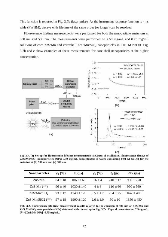
72
This function is reported in Fig. 3.7b (laser pulse). As the instrument response function is 4 ns
wide (FWHM), decays with lifetime of the same order (or longer) can be resolved.
Fluorescence lifetime measurements were performed for both the nanoparticle emissions at
380 nm and 590 nm. The measurements were performed on 7.50 mg/mL and 0.75 mg/mL
solutions of core ZnS:Mn and core/shell ZnS:Mn/SiO2 nanoparticles in 0.01 M NaOH. Fig.
3.7b and c show examples of these measurements for core-shell nanoparticles at the higher
concentration.
(b)
(a)
(c)
Fig. 3.7. (a) Set-up for fluorescence lifetime measurements @CNRS of Mulhouse. Fluorescence decays of ZnS:Mn/SiO2 nanoparticles (NPs) 7.50 mg/mL concentrated in water containing 0.01 M NaOH for the emission at (b) 590 nm and (c) 380 nm.
Nanoparticles ϕ1 (%) τ1 (µs) ϕ2 (%) τ2 (µs) <τ> (µs)
ZnS:Mn 84 ± 18 1060 ± 60 16 ± 4 240 ± 17 930 ± 250
ZnS:Mn (**) 96 ± 40 1030 ± 140 4 ± 4 110 ± 60 990 ± 560
ZnS:Mn/SiO2 93 ± 17 1740 ± 120 6.5 ± 1.7 254 ± 25 1640± 400
ZnS:Mn/SiO2 (**) 97 ± 18 1900 ± 120 2.6 ± 1.0 50 ± 10 1850 ± 450
Tab. 3.2. Fluorescence life time measurement results relative to the emission at 590 nm of ZnS:Mn and ZnS:Mn/SiO2 nanoparticles (NPs) obtained with the set up in Fig. 3.7a. Typical concentration 7.5mg/mL; (**) [ZnS:Mn NPs]=0.75 mg/mL.
73
The data were treated with the same software and the same procedure as the data collected
at CSEM for all the emissions at 590 nm. The curves were not deconvoluted from the
instrument response function due to the long decay constant. However, the data in the interval
0.0 ms < t < 1.2 ms were excluded from the data analysis. The curves were fitted to a double
exponential decay and the results are shown in Tab. 3.2.
The long fluorescence lifetime component contributes ∼90% of the steady state
fluorescence for all the samples. For the core nanoparticles the lifetime values obtained in
CSEM and at the CNRS are identical, to within experimental errors. However, the lifetime
measured for the core/shell nanoparticles at the CNRS are slightly longer than the values
obtained at CSEM. The reasons for this difference are not clear.
The fluorescence emission at 380 nm was also measured for all the samples. As the
lifetime values were in the nanosecond range, the data were deconvoluted from the instrument
response function before treatment. The data were fitted to a double exponential decay and the
results are shown in Tab. 3.3. The data analysis was performed at Mulhouse and the errors on
the αi values were neglected in the error propagation treatment. Core and core/shell
nanoparticles are found to have an average fluorescence lifetime of respectively ∼4 ns and
∼10 ns.
Nanoparticles ϕ1 (%) τ1 (ns) ϕ2 (%) τ2 (ns) <τ> (ns)
ZnS:Mn 72 ± 5 0.77 ± 0.01 28 ± 2 11.78± 0.08 3.9 ± 0.3
ZnS:Mn (**) 66.4 ± 1.5 1.085 ± 0.005 33.6 ± 0.7 9.50 ±0.02 3.91 ± 0.09
ZnS:Mn/SiO2 52.0 ± 0.4 1.776 ± 0.007 48.0 ± 0.3 24.60 ± 0.08 12.73 ± 0.13
ZnS:Mn/SiO2 (**) 62 ± 3 1.90 ± 0.05 38 ± 1 20.96 ± 0.08 9.1 ± 0.3
Tab. 3.3. Fluorescence lifetime measurement results relative to the emission at 380 nm of ZnS:Mn and ZnS:Mn/SiO2 nanoparticles (NPs) obtained with the set up in Fig. 3.7a. Typical concentration 7.5mg/mL. (**) [ZnS:Mn NPs]=0.75 mg/mL.
3.3.6 Conclusions
Core and core-shell ZnS:Mn nanoparticles exhibited long fluorescence lifetimes and high
resistance to photobleaching. Their performances were compared with europium
luminescence FluoSphere beads which are well known for their long fluorescence lifetimes
and their high resistance to photobleaching. The nanoparticles exhibit longer fluorescence
lifetime, while their resistance to photobleaching was slightly lower. The semiconductor
nanoparticles exhibited these excellent properties both in solution and in the dry state.
74
The decay curve for the orange emission of core nanoparticles showed a double
exponential decay with an initial fast decay (τ ~ 100 µs), followed by a slow decay with a
decay time of 670 µs. Decay time measurements for the orange emission of the core/shell
nanoparticles show that, after an initial fast decay (τ ~ 150 µs), a slow single exponential
decay with a decay time of 900 µs is present. Fluorescence lifetime measurements were
repeated with a more sophisticated instrumentation in the CNRS of Mulhouse. While the
same values were found for core nanoparticle fluorescent lifetime to within the experimental
errors, core/shell nanoparticles exhibited a longer decay, characterized by a first fast decay
time of ~ 150 µs and a longer decay time of 1.8 ms. These last results are in agreement with
the decays of ZnS:Mn emission observed by other groups [135;136].
In the measurements performed in CSEM and CMRS, longer fluorescence lifetimes were
found for core/shell nanoparticles compared to core nanoparticles both for the bulk and for the
dopant emission. Moreover, the core-shell nanoparticles’ quantum yield is higher than the
core nanoparticles’ quantum yield [109]. The reasons for this behaviour may be found in the
surface states of the nanoparticles. The main degradation mechanism for semiconductor
nanoparticles is the photo-oxidation of the surface that causes the formation of electron traps,
leading to a decrease in the number of emitted photons. One of the solutions to this problem
consists in capping the nanocrystal with an inorganic shell that binds to the core, minimizing
the number of defects at its surface [137]. The shell saturates some electron traps at the
surface of the nanoparticle core from where the electrons recombined non-radiatively. If these
traps are reduced the quantum yield increases because a higher number of electrons
participates to the fluorescence emission; the increase of the lifetime is due to the suppression
of the trap recombination, which was an additional rate process that depopulated the excited
state.
A change of the nanoparticle’s fluorescence lifetime was expected when comparing the
two states in which the nanoparticles are surrounded by solvent molecules and in which they
are dried on the substrate [134]. Core nanoparticles have in fact their surface electronic states
exposed to the external environment, although a shell of organic molecules covers the surface.
Thus, it was expected that the surrounding molecules could influence the electron relaxation
rate relative to surface states. On the contrary, no effect was observed. We hypothesize that
this organic shell may be sufficient to completely mask the core from the environment.
Alternatively, the set up may be not enough sensitive to detect these changes.
75
The possibility of performing time-gated fluorescence detection with ZnS:Mn
nanoparticles was explored; thanks to their performances, a simple and cheap set-up for time-
gated fluorescence intensity measurements was realized in CSEM and first feasibility
measurements were performed. The nanoparticles exhibit fluorescence signals well above the
background and their emission could be clearly distinguished from that of the environment.
3.4 Nanoparticles used with waveguide-based sensors
In 3.2 sensors based on thin-film planar waveguide technology were introduced as
biosensors able to fulfil the demand for high sensibility, reduced sample and reagent
consumption and increasing degree of multiplexing capability. The possibility to use ZnS:Mn
nanoparticles in combination with this kind of sensors will be thus explored in this section, as
a promising line of development for innovating biosensors.
One route for the improvement of waveguide-based sensor sensitivity and accuracy is the
combination of fluorescence and refractometric detection. However, this requires that the
fluorescence labels are clearly detectable by refractometric measurements. We will
demonstrate that the ZnS:Mn nanoparticles can be used as mass labels for waveguide-based
refractometric sensors.
For this scope, sensor surfaces were functionalized to selectively bind the ZnS:Mn
nanoparticles on one channel. The surface functionalization should fulfil two conditions: the
measurement and the reference pads, that respectively adsorb and do not adsorb the
nanoparticles, should be created on the same chip; the nanoparticles should be organized
within some 200 nm from the waveguide film surface in order to be excited by the evanescent
field.
Many solutions exist to realize surface functionalizations having the required properties.
As the nanoparticles present a net negative charge at the surface due to the L-cysteine
molecules of their protective organic shell (see Fig. 2.2a), we propose a waveguide
functionalization technique based on the electrostatic interaction between the nanoparticles
and the waveguide surface. The example described below involves the organization of the
nanoparticles using polyelectrolytes.
3.4.1 Waveguide surface functionalization
The surface functionalization was performed on the channels of a waveguide-based sensor
chip and the selective adsorption of ZnS:Mn nanoparticles on one channel was demonstrated.

76
This technique was applied to a WIOS sensor chip and monitored using the WIOS instrument
itself.
The channel functionalization was achieved by means of polyelectrolytes. These polymers
have ionisable monomers and in polar solvents, such as water, dissociate into charged
polymers and small counter-ions of opposite sign. They are of widespread importance with
many applications in physics, biology and chemistry. The behaviour of polyelectrolytes is
theoretically quite poorly understood, chiefly because it is difficult to deal with their long-
range coulomb interactions. In addition, counter-ions, complex-formation, salt and their
differing length-scales make comparison between theory and experiments difficult because of
questions of the validity of the theories in different regimes [138]. Multilayer structures can
be built on solid substrate via a series of adsorption processes using positively and negatively
charged polyelectrolytes (respectively polycations and polyanions) [139]. As shown in Fig.
3.8, a layer of polycation molecules is first adsorbed on a negatively charged surface. Then
the surface is abundantly rinsed to remove the molecules that are not specifically bound. As a
result, a net positive charge is distributed over the whole surface and now polyanion
molecules can be adsorbed on the surface, conferring a net negative charge to the bilayer
surface. Repetition of the two adsorption steps leads to the formation of a multilayer structure.
Fig. 3.8. Simplified molecular picture of two polyelectrolyte adsorption steps starting with a negatively charged surface.
The WIOS sensor chip is provided with four measurement channels (for simplicity only
two channels will be considered in the following description). Polyelectrolytes were used to
confer different electrostatic characters to the channels and the structure was thus limited to
one or two polymer layers. PEI and PSS molecules were diluted in MilliQ water containing
0.5 M NaCl, respectively in concentrations of 0.6 mg/mL and 0.25 mg/mL. All the solutions
used during the experiment were stored next to the sensor instrument one hour before use in
order to equilibrate the temperatures and minimize the effects due to temperature variations in
the measurements. A double flow cell placed on the sensor chip allowed the physical
separation of the two channels so that they could be functionalized separately. WIOS
measures the change in the waveguide effective refractive index that is induced, in the case of
77
these measurements, by two main factors: the adsorption of molecules to the waveguide
surface and the change of the refractive index of the solution. To eliminate the last
contribution, MilliQ water was taken as standard solution and the cells were filled with it
before and after each adsorption process. The solution was introduced into the cells using a
pipette and was extracted via a fluidic system equipped with a pump.
Fig. 3.9 shows the WIOS measurement acquired during the channel functionalization. The
effective refractive index variation is shown, in arbitrary units called WIOS units (see below),
as a function of the time. The areas dashed in grey correspond to the measurements performed
with pure MilliQ water and quantitative comparison can only be made between data in these
regions. MilliQ water was first introduced in both the cells and a baseline was taken for the
two channels. Then 150 µL of PEI solution was introduced into both the cells and the signal
abruptly increased. The signal variation is in part due to the change of the solution refractive
index, and in part to the adsorption on the surface of the PEI molecules. The pads were
abundantly rinsed with water and the signal decreased to about 40 units which are due to the
adlayer of PEI. The reduction of 60 WIOS units on washing may be due, in part, to the
removal of molecules not strongly adsorbed to the surface and in part to the different
refractive indexes of the solution above the adlayer.
Fig. 3.9. Channel functionalization: channel 1 is coated with a PEI layer and channel 2 with a bilayer PEI+PSS. Channel 1 result at its surface positively charged and channel 2 negatively.
150 µL of PSS solution were then introduced into the cell 2, while MilliQ water was kept
in the other cell. The signal of channel 2 increased due to the adsorption of PSS molecules,
while cannel 1’s signal remained constant. After rinsing, the PSS adlayer resulted in a total
increase in the effective refractive index of about 70 WIOS units. At this point, the surface of
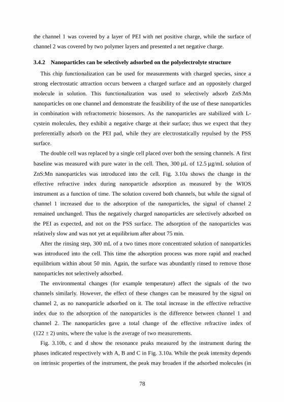
78
the channel 1 was covered by a layer of PEI with net positive charge, while the surface of
channel 2 was covered by two polymer layers and presented a net negative charge.
3.4.2 Nanoparticles can be selectively adsorbed on the polyelectrolyte structure
This chip functionalization can be used for measurements with charged species, since a
strong electrostatic attraction occurs between a charged surface and an oppositely charged
molecule in solution. This functionalization was used to selectively adsorb ZnS:Mn
nanoparticles on one channel and demonstrate the feasibility of the use of these nanoparticles
in combination with refractometric biosensors. As the nanoparticles are stabilized with L-
cystein molecules, they exhibit a negative charge at their surface; thus we expect that they
preferentially adsorb on the PEI pad, while they are electrostatically repulsed by the PSS
surface.
The double cell was replaced by a single cell placed over both the sensing channels. A first
baseline was measured with pure water in the cell. Then, 300 µL of 12.5 µg/mL solution of
ZnS:Mn nanoparticles was introduced into the cell. Fig. 3.10a shows the change in the
effective refractive index during nanoparticle adsorption as measured by the WIOS
instrument as a function of time. The solution covered both channels, but while the signal of
channel 1 increased due to the adsorption of the nanoparticles, the signal of channel 2
remained unchanged. Thus the negatively charged nanoparticles are selectively adsorbed on
the PEI as expected, and not on the PSS surface. The adsorption of the nanoparticles was
relatively slow and was not yet at equilibrium after about 75 min.
After the rinsing step, 300 mL of a two times more concentrated solution of nanoparticles
was introduced into the cell. This time the adsorption process was more rapid and reached
equilibrium within about 50 min. Again, the surface was abundantly rinsed to remove those
nanoparticles not selectively adsorbed.
The environmental changes (for example temperature) affect the signals of the two
channels similarly. However, the effect of these changes can be measured by the signal on
channel 2, as no nanoparticle adsorbed on it. The total increase in the effective refractive
index due to the adsorption of the nanoparticles is the difference between channel 1 and
channel 2. The nanoparticles gave a total change of the effective refractive index of
(122 ± 2) units, where the value is the average of two measurements.
Fig. 3.10b, c and d show the resonance peaks measured by the instrument during the
phases indicated respectively with A, B and C in Fig. 3.10a. While the peak intensity depends
on intrinsic properties of the instrument, the peak may broaden if the adsorbed molecules (in
79
this case the nanoparticles) absorb or scatter the guided light, compromising the measurement
results. The widths of the peaks acquired before and after nanoparticle adsorption were found
to be identical ((37 ± 2) units) and it is thus concluded that the nanoparticles do not absorb or
scatter the laser light.
(a)
(b)
(c)
(d)
Fig. 3.10. (a) WIOS measurement of the adsorption of semiconductor nanoparticles: channel 1 is functionalized with PEI and experiences nanoparticle adsorption, while channel two, functionalized with PSS is the reference pad. The WIOS resonance peaks of the two channels relative to areas A, B and C are shown in (b), (c) and (d) respectively.
A calibration of the instrument is required to make quantitative measurements of the mass
adsorbed at the surface, i. e. to convert the WIOS units in adsorbed nanoparticle weight per
unit area. This calibration depends on the refractive index of the adlayer on the waveguide
surface and thus should be performed specifically for the analyte and the label to be used.
It is possible to get a rough estimate of it for the measurement shown in Fig. 3.10. If we
hypothesize that the nanoparticles are densely packed on the sensor surface and that each
nanoparticle (NP) covers in projection a circle of 7 nm in diameter, we estimate a nanoparticle
surface density of 2.0×10¹⁰ NPs/mm2. However, this value is an overestimate of the real one,
since the nanoparticles are not densely packed on the surface, but actually assume a random
80
distribution. The Random Sequential Adsorption model [140] indicates that non-interacting
hard spheres irreversibly adsorbing on a flat surface cover 55% of it before reaching an
equilibrium in which no more spheres can reach the surface. The adsorption of the ZnS
nanoparticles is random and sequential, thus the model can be applied as a first
approximation; however, they are negatively charged, a fact that implies a reduction of the
maximal covered surface [140]. Thus, we expect an order of magnitude of 1010 NPs/mm2
adsorbed on the surface. AFM investigation of the sensor chip after nanoparticle adsorption
can be used to determine the correct surface coverage value.
Schematizing the nanoparticle as a homogeneous ZnS sphere 5 nm in diameter gives a
surface mass density of about 2×10³ pg/mm2. The total signal variation due to the adsorption
of the nanoparticles at the equilibrium was 122 WIOS units. Thus, the conversion
1 WIOS unit ~ 15 pg/mm2 is obtained.
3.4.3 Conclusions
We demonstrated that ZnS:Mn nanoparticles can be used as mass labels in refractometric
sensing techniques. The sensing and the reference channels of a waveguide-based sensor chip
were functionalized using polyelectrolytes and the adsorption selectivity was determined by
the different electrostatic interaction between the nanoparticles and the charged channel
surfaces. The nanoparticles were selectively adsorbed on one channel and refractometric
measurements were performed. The WIOS instrument was used for the chip surface
functionalization and the adsorption measurements. However, the described functionalization
does not depend on the instrument used and can be applied as a general method to prepare
sensor surfaces; for example, the polyelectrolytes can be deposited on the surface pads by
microfluidics.
In the present work, polyelectrolytes were used to confer a net electric charge to the sensor
surface. The structures described here were limited to one or two layers, but there are no
theoretical constraints that limit the building of a polymer multilayer on the sensor surface, if
the structure remains confined within some 200 nm from the waveguide film surface. The
possibility to choose the number of polymer layers and thus choose the polymer structure
thickness can be used as a further degree of freedom to control the interactions between the
substrate and any adsorbed molecules. Moreover, this technique allows the incorporation of
different kinds of charged species within the multilayer structure to confer precise
functionalities to the multilayers.

81
3.5 Conclusions
Core and core/shell ZnS:Mn nanoparticles were found to possess exceptionally long
fluorescence lifetimes in the ms range; their performances in terms of long fluorescence
lifetime and photostability were compared with europium-luminescent beads and were shown
to be comparable.
The possibility of using these nanoparticles as probes for time-gated fluorescence detection
was demonstrated. In particular, an extremely simple and cheap instrument was successfully
used to perform these measurements: the excitation source consisted of a flash lamp whose
radiation was filtered in order to match the nanoparticle absorption spectrum, while the
acquisition was performed by standard photodetectors. This was possible thanks to the
fluorescence performances of the nanoparticles.
Most known red and near-infrared emitting probes display lifetimes below 4 ns and short
Stokes shifts. The scattered light (most difficult to eliminate at wavelengths close to the
excitation) and environmental auto-fluorescence (lifetimes in the ns range) affect the signal-
to-noise ratio and cannot be significantly improved with time-gated detection [141]. ZnS:Mn
nanoparticles are red emitting probes characterized, instead, by a large Stokes shift and long
fluorescence lifetime. Thus, these nanoparticles present the novel combination of a red
emission with a long fluorescence lifetime and a high signal-to noise ratio when used in
sensing applications. Unfortunately, this advantage is off-set by the excitation frequency in
the UV that is inconvenient because of an extremely high fluorescence background.
Recently, waveguide-based sensors received the attention of many industries involved in
the development of high performance diagnostic and screening technologies thanks to their
high sensibility and reduced sample and reagent consumption. The use of semiconductor
nanoparticles in combination with this kind of sensors for refractometric measurements was
explored. The sensor chip was functionalized to specifically adsorb the nanoparticles on the
sensing channels within 200 nm from the surface sensor surface. In addition, the reference
channel was functionalized in order to avoid nanoparticle binding on its surface. The sensor
channels were functionalized with differently charged polyelectrolytes in order to confer them
an opposite electrostatic behaviour. Selective adsorption of the nanoparticles on one channel
of the sensor was demonstrated.
A route for the improvement of waveguide-based sensor sensitivity and accuracy is the
combination of fluorescence and refractometric detection. However, fluorescence labels
clearly detectable by refractometric measurements are required. In the specific case of

82
ZnS:Mn nanoparticles, which absorb UV light, a compact waveguide-based sensor may be
developed using an excitation source external to the waveguide. The nanoparticles should
adsorb within 200 nm from the sensor surface and, once excited, their orange emission could
be collected by the waveguide itself. Alternatively, external excitation source and detection
system can be used, with the same set up described in 3.3.1. The combination of
refractometric and fluorescence measurements opens the possibility to higher sensor
accuracies.
83
Chapter 4
4 Organizing Nanoparticles via
Polymer Demixing
Section 1.1.1 described how two immiscible polymers form two separate phases when
dissolved in the same solvent and subjected to solvent evaporation. This phenomenon has
been used to realize structured polymer films with typical feature size ranging from the
micrometer to the nanometer length scale. Examples of such structures were shown in 2.6.1.
The aim of this chapter is to demonstrate the possibility to form patterns of nanoparticles
using polymer demixing. The nanoparticles are initially mixed with the polymer molecules in
the same solution and they end up embedded in the polymer film. The nanoparticles are
patterned in micrometer and sub-micrometer sized features.
4.1 Principle
The aim of this study was to use polymer demixing to form patterns of nanoparticles
embedded in the polymer film. The presence of nano-filler inside the polymer blends was
extensively studied in the past by numerical simulations. In spite of the lack of experimental
results, numerical simulations agreed in distinguishing two main cases concerning the
distribution of the filler particles respect to the polymer phases:
• if the particles do not have a preferential affinity for one of the polymers they will
end up at the interfaces between the polymer phases [59;61].
• if the particles present a better affinity for one of the polymers they will be
distributed mainly in the phase enriched in this polymer [59;60].
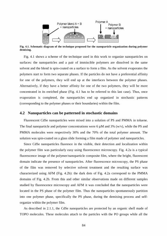
84
Fig. 4.1. Schematic diagram of the technique proposed for the nanoparticle organization during polymer demixing.
Fig. 4.1 shows a scheme of the technique used in this work to organize nanoparticles on
surfaces: the nanoparticles and a pair of immiscible polymers are dissolved in the same
solvent and the blend is spin-coated on a surface to form a film. As the solvent evaporates the
polymers start to form two separate phases. If the particles do not have a preferential affinity
for one of the polymers, they will end up at the interfaces between the polymer phases.
Alternatively, if they have a better affinity for one of the two polymers, they will be more
concentrated in its enriched phase (Fig. 4.1 has to be referred to this last case). Thus, once
evaporation is completed, the nanoparticles end up organized in stochastic patterns
(corresponding to the polymer phases or their boundaries) within the film.
4.2 Nanoparticles can be patterned in stochastic domains
Fluorescent CdSe nanoparticles were mixed into a solution of PS and PMMA in toluene.
The final nanoparticle and polymer concentrations were 6 µM and 3% (w/v), while the PS and
PMMA molecules were respectively 30% and the 70% of the total polymer amount. The
solution was spin-coated on a glass slide forming a film made of polymer and nanoparticles.
Since CdSe nanoparticles fluoresce in the visible, their detection and localization within
the polymer film was particularly easy using fluorescence microscopy. Fig. 4.2a is a typical
fluorescence image of the polymer/nanoparticle composite film, where the bright, fluorescent
domain indicate the presence of nanoparticles. After fluorescence microscopy, the PS phase
of the film was removed by selective solvent treatment and the resulting surface was
characterized using AFM (Fig. 4.2b): the dark dots of Fig. 4.2a correspond to the PMMA
domains of Fig. 4.2b. From this and other similar observations made on different samples
studied by fluorescence microscopy and AFM it was concluded that the nanoparticles were
located in the PS phase of the polymer film. Thus the nanoparticles spontaneously partition
into one polymer phase, specifically the PS phase, during the demixing process and self-
organize within the polymer film.
As described in 2.1.1, the CdSe nanoparticles are protected by an organic shell made of
TOPO molecules. These molecules attach to the particles with the PO groups while all the
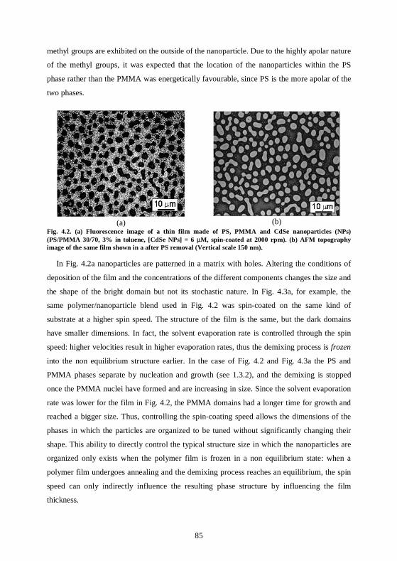
85
methyl groups are exhibited on the outside of the nanoparticle. Due to the highly apolar nature
of the methyl groups, it was expected that the location of the nanoparticles within the PS
phase rather than the PMMA was energetically favourable, since PS is the more apolar of the
two phases.
(a)
(b)
Fig. 4.2. (a) Fluorescence image of a thin film made of PS, PMMA and CdSe nanoparticles (NPs) (PS/PMMA 30/70, 3% in toluene, [CdSe NPs] = 6 µM, spin-coated at 2000 rpm). (b) AFM topography image of the same film shown in a after PS removal (Vertical scale 150 nm).
In Fig. 4.2a nanoparticles are patterned in a matrix with holes. Altering the conditions of
deposition of the film and the concentrations of the different components changes the size and
the shape of the bright domain but not its stochastic nature. In Fig. 4.3a, for example, the
same polymer/nanoparticle blend used in Fig. 4.2 was spin-coated on the same kind of
substrate at a higher spin speed. The structure of the film is the same, but the dark domains
have smaller dimensions. In fact, the solvent evaporation rate is controlled through the spin
speed: higher velocities result in higher evaporation rates, thus the demixing process is frozen
into the non equilibrium structure earlier. In the case of Fig. 4.2 and Fig. 4.3a the PS and
PMMA phases separate by nucleation and growth (see 1.3.2), and the demixing is stopped
once the PMMA nuclei have formed and are increasing in size. Since the solvent evaporation
rate was lower for the film in Fig. 4.2, the PMMA domains had a longer time for growth and
reached a bigger size. Thus, controlling the spin-coating speed allows the dimensions of the
phases in which the particles are organized to be tuned without significantly changing their
shape. This ability to directly control the typical structure size in which the nanoparticles are
organized only exists when the polymer film is frozen in a non equilibrium state: when a
polymer film undergoes annealing and the demixing process reaches an equilibrium, the spin
speed can only indirectly influence the resulting phase structure by influencing the film
thickness.
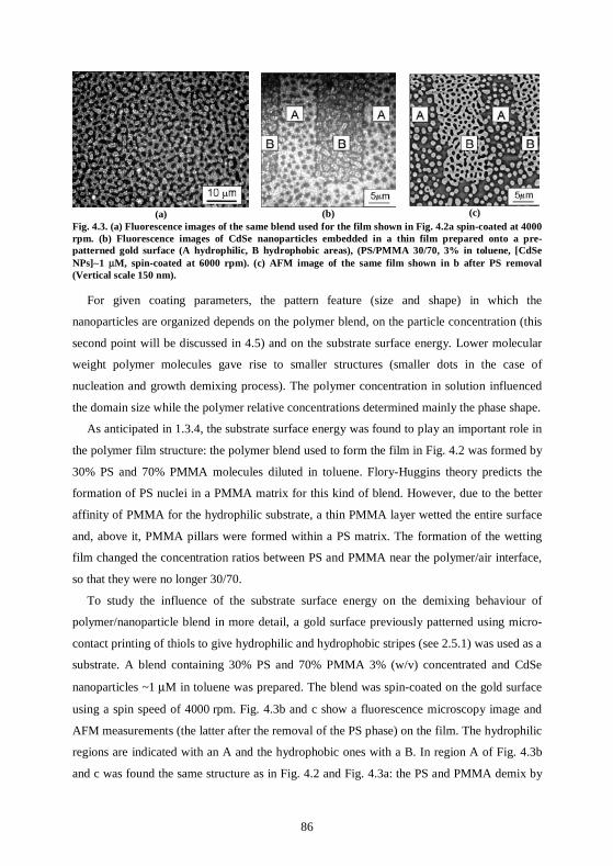
86
(a)
(b)
(c)
Fig. 4.3. (a) Fluorescence images of the same blend used for the film shown in Fig. 4.2a spin-coated at 4000 rpm. (b) Fluorescence images of CdSe nanoparticles embedded in a thin film prepared onto a pre-patterned gold surface (A hydrophilic, B hydrophobic areas), (PS/PMMA 30/70, 3% in toluene, [CdSe NPs]∼1 µM, spin-coated at 6000 rpm). (c) AFM image of the same film shown in b after PS removal (Vertical scale 150 nm).
For given coating parameters, the pattern feature (size and shape) in which the
nanoparticles are organized depends on the polymer blend, on the particle concentration (this
second point will be discussed in 4.5) and on the substrate surface energy. Lower molecular
weight polymer molecules gave rise to smaller structures (smaller dots in the case of
nucleation and growth demixing process). The polymer concentration in solution influenced
the domain size while the polymer relative concentrations determined mainly the phase shape.
As anticipated in 1.3.4, the substrate surface energy was found to play an important role in
the polymer film structure: the polymer blend used to form the film in Fig. 4.2 was formed by
30% PS and 70% PMMA molecules diluted in toluene. Flory-Huggins theory predicts the
formation of PS nuclei in a PMMA matrix for this kind of blend. However, due to the better
affinity of PMMA for the hydrophilic substrate, a thin PMMA layer wetted the entire surface
and, above it, PMMA pillars were formed within a PS matrix. The formation of the wetting
film changed the concentration ratios between PS and PMMA near the polymer/air interface,
so that they were no longer 30/70.
To study the influence of the substrate surface energy on the demixing behaviour of
polymer/nanoparticle blend in more detail, a gold surface previously patterned using micro-
contact printing of thiols to give hydrophilic and hydrophobic stripes (see 2.5.1) was used as a
substrate. A blend containing 30% PS and 70% PMMA 3% (w/v) concentrated and CdSe
nanoparticles ~1 µM in toluene was prepared. The blend was spin-coated on the gold surface
using a spin speed of 4000 rpm. Fig. 4.3b and c show a fluorescence microscopy image and
AFM measurements (the latter after the removal of the PS phase) on the film. The hydrophilic
regions are indicated with an A and the hydrophobic ones with a B. In region A of Fig. 4.3b
and c was found the same structure as in Fig. 4.2 and Fig. 4.3a: the PS and PMMA demix by
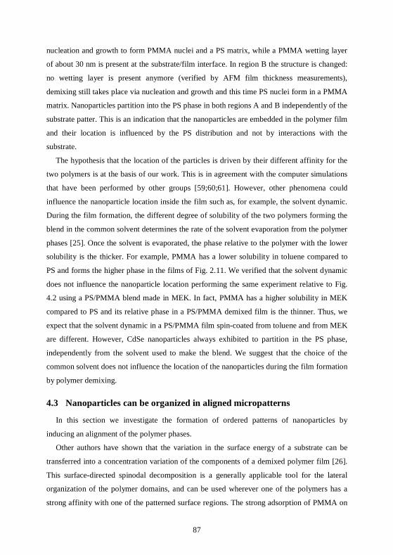
87
nucleation and growth to form PMMA nuclei and a PS matrix, while a PMMA wetting layer
of about 30 nm is present at the substrate/film interface. In region B the structure is changed:
no wetting layer is present anymore (verified by AFM film thickness measurements),
demixing still takes place via nucleation and growth and this time PS nuclei form in a PMMA
matrix. Nanoparticles partition into the PS phase in both regions A and B independently of the
substrate patter. This is an indication that the nanoparticles are embedded in the polymer film
and their location is influenced by the PS distribution and not by interactions with the
substrate.
The hypothesis that the location of the particles is driven by their different affinity for the
two polymers is at the basis of our work. This is in agreement with the computer simulations
that have been performed by other groups [59;60;61]. However, other phenomena could
influence the nanoparticle location inside the film such as, for example, the solvent dynamic.
During the film formation, the different degree of solubility of the two polymers forming the
blend in the common solvent determines the rate of the solvent evaporation from the polymer
phases [25]. Once the solvent is evaporated, the phase relative to the polymer with the lower
solubility is the thicker. For example, PMMA has a lower solubility in toluene compared to
PS and forms the higher phase in the films of Fig. 2.11. We verified that the solvent dynamic
does not influence the nanoparticle location performing the same experiment relative to Fig.
4.2 using a PS/PMMA blend made in MEK. In fact, PMMA has a higher solubility in MEK
compared to PS and its relative phase in a PS/PMMA demixed film is the thinner. Thus, we
expect that the solvent dynamic in a PS/PMMA film spin-coated from toluene and from MEK
are different. However, CdSe nanoparticles always exhibited to partition in the PS phase,
independently from the solvent used to make the blend. We suggest that the choice of the
common solvent does not influence the location of the nanoparticles during the film formation
by polymer demixing.
4.3 Nanoparticles can be organized in aligned micropatterns
In this section we investigate the formation of ordered patterns of nanoparticles by
inducing an alignment of the polymer phases.
Other authors have shown that the variation in the surface energy of a substrate can be
transferred into a concentration variation of the components of a demixed polymer film [26].
This surface-directed spinodal decomposition is a generally applicable tool for the lateral
organization of the polymer domains, and can be used wherever one of the polymers has a
strong affinity with one of the patterned surface regions. The strong adsorption of PMMA on
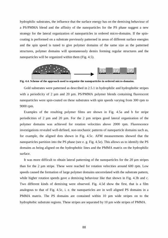
88
hydrophilic substrates, the influence that the surface energy has on the demixing behaviour of
a PS/PMMA blend and the affinity of the nanoparticles for the PS phase suggest a new
strategy for the lateral organization of nanoparticles in ordered micro-domains. If the spin-
coating is performed on a substrate previously patterned in areas of different surface energies
and the spin speed is tuned to give polymer domains of the same size as the patterned
structures, polymer domains will spontaneously demix forming regular structures and the
nanoparticles will be organized within them (Fig. 4.5).
Fig. 4.4. Scheme of the approach used to organize the nanoparticles in ordered micro-domains.
Gold substrates were patterned as described in 2.5.1 in hydrophilic and hydrophobic stripes
with a periodicity of 2 µm and 20 µm. PS/PMMA polymer blends containing fluorescent
nanoparticles were spin-coated on these substrates with spin speeds varying from 300 rpm to
9000 rpm.
Examples of the resulting polymer films are shown in Fig. 4.5a and b for stripe
periodicities of 2 µm and 20 µm. For the 2 µm stripes good lateral organization of the
polymer domains was achieved for rotation velocities above 2000 rpm. Fluorescence
investigations revealed well-defined, non-stochastic patterns of nanoparticle domains such as,
for example, the aligned dots shown in Fig. 4.5c. AFM measurements showed that the
nanoparticles partition into the PS phase (see e. g. Fig. 4.5e). This allows us to identify the PS
domains as being aligned on the hydrophobic lines and the PMMA matrix on the hydrophilic
surface.
It was more difficult to obtain lateral patterning of the nanoparticles for the 20 µm stripes
than for the 2 µm stripe. These were reached for rotation velocities around 600 rpm. Low
speeds caused the formation of large polymer domains uncorrelated with the substrate pattern,
while higher rotation speeds gave a demixing behaviour like that shown in Fig. 4.3b and c.
Two different kinds of demixing were observed. Fig. 4.5d show the first, that is a film
analogous to that of Fig. 4.5c, i. e. the nanoparticles are in well aligned PS domains in a
PMMA matrix. The PS domains are contained within 10 µm wide stripes on to the
hydrophobic substrate regions. These stripes are separated by 10 µm wide stripes of PMMA.
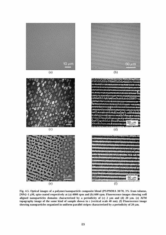
89
(a)
(b)
(c)
(d)
(e)
(f)
Fig. 4.5. Optical images of a polymer/nanoparticle composite blend (PS/PMMA 30/70, 3% from toluene, [NPs]∼1 µM, spin-coated respectively at (a) 4000 rpm and (b) 600 rpm. Fluorescence images showing well aligned nanoparticles domains characterized by a periodicity of (c) 2 µm and (d) 20 µm. (e) AFM topography image of the same kind of sample shown in c (vertical scale 40 nm). (f) Fluorescence image showing nanoparticles organized in uniform parallel stripes characterized by a periodicity of 20 µm.
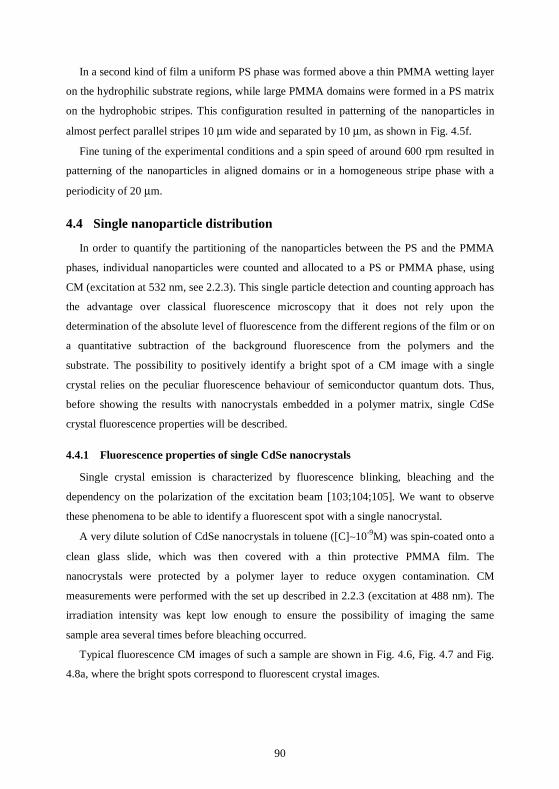
90
In a second kind of film a uniform PS phase was formed above a thin PMMA wetting layer
on the hydrophilic substrate regions, while large PMMA domains were formed in a PS matrix
on the hydrophobic stripes. This configuration resulted in patterning of the nanoparticles in
almost perfect parallel stripes 10 µm wide and separated by 10 µm, as shown in Fig. 4.5f.
Fine tuning of the experimental conditions and a spin speed of around 600 rpm resulted in
patterning of the nanoparticles in aligned domains or in a homogeneous stripe phase with a
periodicity of 20 µm.
4.4 Single nanoparticle distribution
In order to quantify the partitioning of the nanoparticles between the PS and the PMMA
phases, individual nanoparticles were counted and allocated to a PS or PMMA phase, using
CM (excitation at 532 nm, see 2.2.3). This single particle detection and counting approach has
the advantage over classical fluorescence microscopy that it does not rely upon the
determination of the absolute level of fluorescence from the different regions of the film or on
a quantitative subtraction of the background fluorescence from the polymers and the
substrate. The possibility to positively identify a bright spot of a CM image with a single
crystal relies on the peculiar fluorescence behaviour of semiconductor quantum dots. Thus,
before showing the results with nanocrystals embedded in a polymer matrix, single CdSe
crystal fluorescence properties will be described.
4.4.1 Fluorescence properties of single CdSe nanocrystals
Single crystal emission is characterized by fluorescence blinking, bleaching and the
dependency on the polarization of the excitation beam [103;104;105]. We want to observe
these phenomena to be able to identify a fluorescent spot with a single nanocrystal.
A very dilute solution of CdSe nanocrystals in toluene ([C]∼10-9M) was spin-coated onto a
clean glass slide, which was then covered with a thin protective PMMA film. The
nanocrystals were protected by a polymer layer to reduce oxygen contamination. CM
measurements were performed with the set up described in 2.2.3 (excitation at 488 nm). The
irradiation intensity was kept low enough to ensure the possibility of imaging the same
sample area several times before bleaching occurred.
Typical fluorescence CM images of such a sample are shown in Fig. 4.6, Fig. 4.7 and Fig.
4.8a, where the bright spots correspond to fluorescent crystal images.
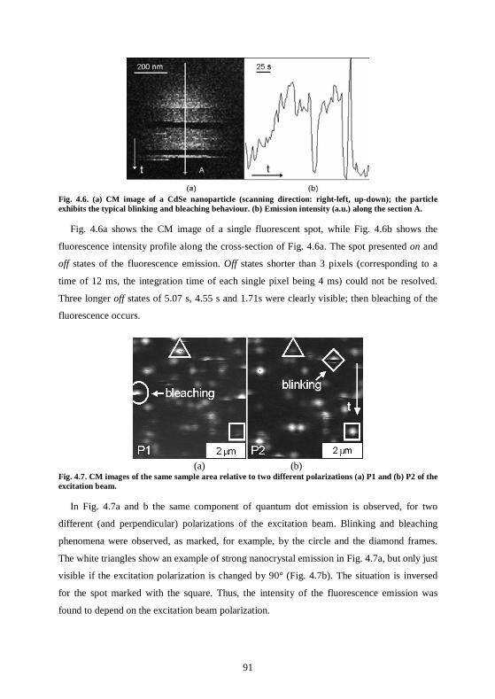
91
Fig. 4.6. (a) CM image of a CdSe nanoparticle (scanning direction: right-left, up-down); the particle exhibits the typical blinking and bleaching behaviour. (b) Emission intensity (a.u.) along the section A.
Fig. 4.6a shows the CM image of a single fluorescent spot, while Fig. 4.6b shows the
fluorescence intensity profile along the cross-section of Fig. 4.6a. The spot presented on and
off states of the fluorescence emission. Off states shorter than 3 pixels (corresponding to a
time of 12 ms, the integration time of each single pixel being 4 ms) could not be resolved.
Three longer off states of 5.07 s, 4.55 s and 1.71s were clearly visible; then bleaching of the
fluorescence occurs.
(a) (b)
Fig. 4.7. CM images of the same sample area relative to two different polarizations (a) P1 and (b) P2 of the excitation beam.
In Fig. 4.7a and b the same component of quantum dot emission is observed, for two
different (and perpendicular) polarizations of the excitation beam. Blinking and bleaching
phenomena were observed, as marked, for example, by the circle and the diamond frames.
The white triangles show an example of strong nanocrystal emission in Fig. 4.7a, but only just
visible if the excitation polarization is changed by 90° (Fig. 4.7b). The situation is inversed
for the spot marked with the square. Thus, the intensity of the fluorescence emission was
found to depend on the excitation beam polarization.
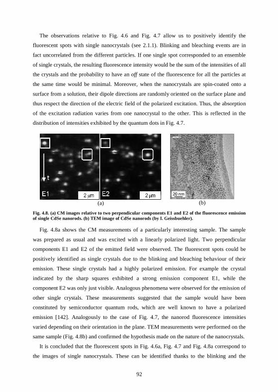
92
The observations relative to Fig. 4.6 and Fig. 4.7 allow us to positively identify the
fluorescent spots with single nanocrystals (see 2.1.1). Blinking and bleaching events are in
fact uncorrelated from the different particles. If one single spot corresponded to an ensemble
of single crystals, the resulting fluorescence intensity would be the sum of the intensities of all
the crystals and the probability to have an off state of the fluorescence for all the particles at
the same time would be minimal. Moreover, when the nanocrystals are spin-coated onto a
surface from a solution, their dipole directions are randomly oriented on the surface plane and
thus respect the direction of the electric field of the polarized excitation. Thus, the absorption
of the excitation radiation varies from one nanocrystal to the other. This is reflected in the
distribution of intensities exhibited by the quantum dots in Fig. 4.7.
(a)
(b)
Fig. 4.8. (a) CM images relative to two perpendicular components E1 and E2 of the fluorescence emission of single CdSe nanorods. (b) TEM image of CdSe nanorods (by I. Geissbuehler).
Fig. 4.8a shows the CM measurements of a particularly interesting sample. The sample
was prepared as usual and was excited with a linearly polarized light. Two perpendicular
components E1 and E2 of the emitted field were observed. The fluorescent spots could be
positively identified as single crystals due to the blinking and bleaching behaviour of their
emission. These single crystals had a highly polarized emission. For example the crystal
indicated by the sharp squares exhibited a strong emission component E1, while the
component E2 was only just visible. Analogous phenomena were observed for the emission of
other single crystals. These measurements suggested that the sample would have been
constituted by semiconductor quantum rods, which are well known to have a polarized
emission [142]. Analogously to the case of Fig. 4.7, the nanorod fluorescence intensities
varied depending on their orientation in the plane. TEM measurements were performed on the
same sample (Fig. 4.8b) and confirmed the hypothesis made on the nature of the nanocrystals.
It is concluded that the fluorescent spots in Fig. 4.6a, Fig. 4.7 and Fig. 4.8a correspond to
the images of single nanocrystals. These can be identified thanks to the blinking and the
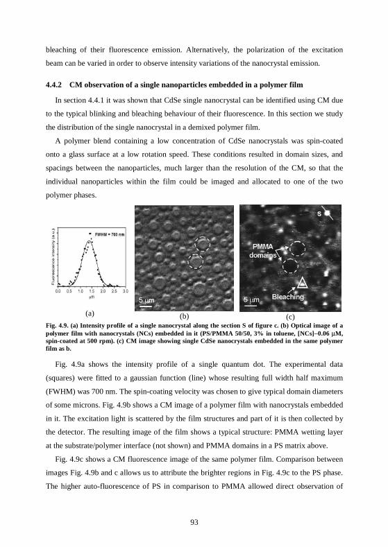
93
bleaching of their fluorescence emission. Alternatively, the polarization of the excitation
beam can be varied in order to observe intensity variations of the nanocrystal emission.
4.4.2 CM observation of a single nanoparticles embedded in a polymer film
In section 4.4.1 it was shown that CdSe single nanocrystal can be identified using CM due
to the typical blinking and bleaching behaviour of their fluorescence. In this section we study
the distribution of the single nanocrystal in a demixed polymer film.
A polymer blend containing a low concentration of CdSe nanocrystals was spin-coated
onto a glass surface at a low rotation speed. These conditions resulted in domain sizes, and
spacings between the nanoparticles, much larger than the resolution of the CM, so that the
individual nanoparticles within the film could be imaged and allocated to one of the two
polymer phases.
(a) (b)
(c)
Fig. 4.9. (a) Intensity profile of a single nanocrystal along the section S of figure c. (b) Optical image of a polymer film with nanocrystals (NCs) embedded in it (PS/PMMA 50/50, 3% in toluene, [NCs]∼0.06 µM, spin-coated at 500 rpm). (c) CM image showing single CdSe nanocrystals embedded in the same polymer film as b.
Fig. 4.9a shows the intensity profile of a single quantum dot. The experimental data
(squares) were fitted to a gaussian function (line) whose resulting full width half maximum
(FWHM) was 700 nm. The spin-coating velocity was chosen to give typical domain diameters
of some microns. Fig. 4.9b shows a CM image of a polymer film with nanocrystals embedded
in it. The excitation light is scattered by the film structures and part of it is then collected by
the detector. The resulting image of the film shows a typical structure: PMMA wetting layer
at the substrate/polymer interface (not shown) and PMMA domains in a PS matrix above.
Fig. 4.9c shows a CM fluorescence image of the same polymer film. Comparison between
images Fig. 4.9b and c allows us to attribute the brighter regions in Fig. 4.9c to the PS phase.
The higher auto-fluorescence of PS in comparison to PMMA allowed direct observation of

94
the microphase structure of the film without additional labelling of the polymers and with no
need of bright field images such as in Fig. 4.9b. The round dark areas in Fig. 4.9c correspond
to PMMA enriched domains, while the lighter regions are the surrounding PS enriched
matrix.
In most cases, the bright spots in Fig. 4.9c with count rates above the usual PS background
can be positively identified as single fluorescent nanocrystals by means of their characteristic
properties like blinking, bleaching and polarization effects. This indicates that, under these
conditions, the majority of the nanoparticles in the film do not aggregate, but are present as
isolated particles.
CM measurements of single crystals embedded in PS films and in PMMA films separately
showed no preferential quenching of the quantum dots fluorescence. Films differing in
polymer composition and nanoparticle concentration have been observed. Of 460
nanoparticles counted, about the 20% of them resulted located in the PMMA phase. However,
it was not possible to establish if the nanoparticles were located in the PMMA phase or in
some PS inclusion inside the PMMA phase because of the limited CM microscopy resolution.
Close study of Fig. 4.3 and Fig. 4.9c suggests that, in addition to the partitioning of the
quantum dots in the PS phase, there may be an enrichment of the nanocrystals at the
interfaces between the PS and PMMA phases. About 30% of nanoparticles were found to be
located at or near this interface. Unfortunately the resolution of CM microscopy does not
allow precise definition of the position of the phase interfaces in these images and requires a
very low concentration of nanoparticles in the film. These two limitations make it very
difficult to come to a definite conclusion on this subject. A more detailed study of the
distribution of the particles within the individual polymer phases of the film requires the use
of AFM or TEM to identify the positions of the individual nanoparticles more precisely.
In conclusion CM observation of a polymer film with nanocrystals embedded in it allowed
the observation of a single crystal distribution in the polymer film. The nanocrystals did not
aggregate. More than 80% of the nanocrystals seemed distributed in the PS phase. About 30%
were located near the interface between PS and PMMA.
4.4.3 AFM observation of single nanoparticle distribution
Single nanoparticle distribution was observed using AFM.
A gold substrate was immersed for 2 hours in a solution of hexadecane thiol molecules
0.5 mM in ethanol, rinsed with ethanol and dried under nitrogen. The resulting substrate was
hydrophobic. Co nanoparticles were mixed into a symmetric blend of PS and PMMA 1%
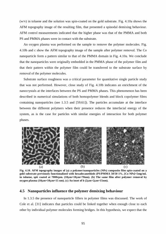
95
(w/v) in toluene and the solution was spin-coated on the gold substrate. Fig. 4.10a shows the
AFM topography image of the resulting film, that presented a spinodal demixing behaviour.
AFM control measurements indicated that the higher phase was that of the PMMA and both
PS and PMMA phases were in contact with the substrate.
An oxygen plasma was performed on the sample to remove the polymer molecules. Fig.
4.10b and c show the AFM topography image of the sample after polymer removal. The Co
nanoparticle form a pattern similar to that of the PMMA domain in Fig. 4.10a. We conclude
that the nanoparticles were originally embedded in the PMMA phase of the polymer film and
that their pattern within the polymer film could be transferred to the substrate surface by
removal of the polymer molecules.
Substrate surface roughness was a critical parameter for quantitative single particle study
that was not performed. However, close study of Fig. 4.10b indicates an enrichment of the
nanocrystals at the interfaces between the PS and PMMA phases. This phenomenon has been
described in numerical simulations of both homopolymer blends and block copolymer films
containing nanoparticles (see 1.3.5 and [59;61]). The particles accumulate at the interface
between the different polymers when their presence reduces the interfacial energy of the
system, as is the case for particles with similar energies of interaction for both polymer
phases.
(a)
(b)
(c)
Fig. 4.10. AFM topography images of (a) a polymer/nanoparticles (NPs) composite film spin-coated on a gold substrate previously functionalized with hexadecanethiols (PS/PMMA 50/50 1%, [Co NPs]=5mg/mL in toluene, spit coated at 7000rpm. (10µm×10µm×70nm). (b) The same film after polymer removal by oxygen plasma (10µm×10µm×15 nm). (c) An inset of b (2µm×2µm×15nm).
4.5 Nanoparticles influence the polymer demixing behaviour
In 1.3.5 the presence of nanoparticle fillers in polymer films was discussed. The work of
Cole et al. [31] indicates that particles could be linked together when enough close to each
other by individual polymer molecules forming bridges. In this hypothesis, we expect that the
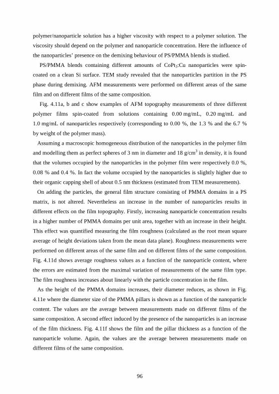
96
polymer/nanoparticle solution has a higher viscosity with respect to a polymer solution. The
viscosity should depend on the polymer and nanoparticle concentration. Here the influence of
the nanoparticles’ presence on the demixing behaviour of PS/PMMA blends is studied.
PS/PMMA blends containing different amounts of CoPt3:Cu nanoparticles were spin-
coated on a clean Si surface. TEM study revealed that the nanoparticles partition in the PS
phase during demixing. AFM measurements were performed on different areas of the same
film and on different films of the same composition.
Fig. 4.11a, b and c show examples of AFM topography measurements of three different
polymer films spin-coated from solutions containing 0.00 mg/mL, 0.20 mg/mL and
1.0 mg/mL of nanoparticles respectively (corresponding to 0.00 %, the 1.3 % and the 6.7 %
by weight of the polymer mass).
Assuming a macroscopic homogeneous distribution of the nanoparticles in the polymer film
and modelling them as perfect spheres of 3 nm in diameter and 18 g/cm3 in density, it is found
that the volumes occupied by the nanoparticles in the polymer film were respectively 0.0 %,
0.08 % and 0.4 %. In fact the volume occupied by the nanoparticles is slightly higher due to
their organic capping shell of about 0.5 nm thickness (estimated from TEM measurements).
On adding the particles, the general film structure consisting of PMMA domains in a PS
matrix, is not altered. Nevertheless an increase in the number of nanoparticles results in
different effects on the film topography. Firstly, increasing nanoparticle concentration results
in a higher number of PMMA domains per unit area, together with an increase in their height.
This effect was quantified measuring the film roughness (calculated as the root mean square
average of height deviations taken from the mean data plane). Roughness measurements were
performed on different areas of the same film and on different films of the same composition.
Fig. 4.11d shows average roughness values as a function of the nanoparticle content, where
the errors are estimated from the maximal variation of measurements of the same film type.
The film roughness increases about linearly with the particle concentration in the film.
As the height of the PMMA domains increases, their diameter reduces, as shown in Fig.
4.11e where the diameter size of the PMMA pillars is shown as a function of the nanoparticle
content. The values are the average between measurements made on different films of the
same composition. A second effect induced by the presence of the nanoparticles is an increase
of the film thickness. Fig. 4.11f shows the film and the pillar thickness as a function of the
nanoparticle volume. Again, the values are the average between measurements made on
different films of the same composition.
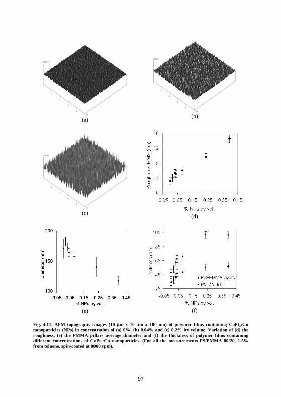
97
(a)
(b)
(c)
(d)
(e)
(f)
Fig. 4.11. AFM topography images (10 µm x 10 µm x 100 nm) of polymer films containing CoPt3:Cu nanoparticles (NPs) in concentration of (a) 0%, (b) 0.04% and (c) 0.2% by volume. Variation of (d) the roughness, (e) the PMMA pillars average diameter and (f) the thickness of polymer films containing different concentrations of CoPt3:Cu nanoparticles. (For all the measurements PS/PMMA 80/20, 1.5% from toluene, spin-coated at 8000 rpm).
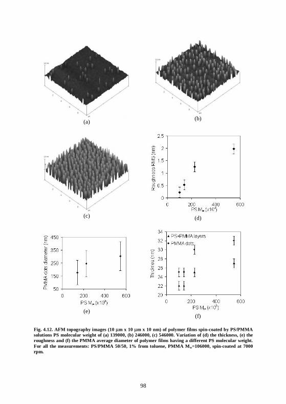
98
(a)
(b)
(c)
(d)
(e)
(f)
Fig. 4.12. AFM topography images (10 µm x 10 µm x 10 nm) of polymer films spin-coated by PS/PMMA solutions PS molecular weight of (a) 139000, (b) 246000, (c) 546000. Variation of (d) the thickness, (e) the roughness and (f) the PMMA average diameter of polymer films having a different PS molecular weight. For all the measurements: PS/PMMA 50/50, 1% from toluene, PMMA Mw=106000, spin-coated at 7000 rpm.
99
In 1.3.5 it was estimated that about 15 polymer molecules are in contact with each
nanoparticle in a film of PS molecules with N∼1000 and nanoparticles with a diameter of
4 nm. This example corresponds well to the films in Fig. 4.11. With the hypothesis that 95%
of the nanoparticles are located in the PS phase or at the interface between the PS and the
PMMA domains (estimated from TEM measurements of the same kind of structures, results
not shown) and that one PS molecule touches no more than one nanoparticle, 77 % of the PS
molecules of the film in Fig. 4.11c would be bound to one nanoparticle. In fact the average
distance between the nanoparticles (calculated assuming a homogeneous distribution in the
polymer film) would be ∼10 nm, which is of the same order of the radius of gyration of the
polymer molecules (Rg = 8.6 nm). Thus, it is probably more realistic that fewer than 77 % of
the polymer molecules touch with one or more nanoparticles.
This would give rise to a reduction in the polymer chain mobility due to the nanoparticles
acting as physical cross-links [30;31]. The increase in nanoparticle concentration inside the
polymer film could be therefore modelled by an augmentation of the polymer molecular
weight.
Experimentally this assumption was tested by polymer demixing of PS/PMMA blends with
different PS molecular weights but equal polymer ratios (by weight). The blends were spin-
coated on Si substrates and AFM measurements were performed. The results are shown in
Fig. 4.12. Increasing the PS molecular weight increases the surface density of PMMA pillars
(Fig. 4.12a, b and c), the film roughness (Fig. 4.12d) and thickness (Fig. 4.12f). The PMMA
pillar diameters do not show a significant variation upon PS molecular weight increasing,
(Fig. 4.12e).
Comparing of Fig. 4.11a, b and c and Fig. 4.12a, b and c we observe and increase of the
PMMA pillar surface density both upon nanoparticle concentration increasing and upon PS
molecular weight increasing. The same behaviour was observed in the case of the film
roughness (comparing Fig. 4.11d and Fig. 4.12d) and thickness (comparing Fig. 4.11f and
Fig. 4.12f). However, the behaviour of the PMMA pillar diameter in the polymer/nanoparticle
composite film and in the proposed model is not the same, as shown by a comparison of Fig.
4.11e with Fig. 4.12e.
Our model was able to reproduce some of the effects induced by the presence of the
nanoparticles on the film topography. This is an indication that the nanoparticles probably do
act as physical links between the polymer molecules. However, the model is not able to
describe in a complete form the phenomena arising in the blend when the nanoparticles are
mixed to the polymer.
100
4.6 Conclusion
A technique for patterning nanoparticles on surfaces has been proposed. This technique is
based on the demixing behaviour of immiscible polymer blends. The nanoparticles are mixed
into a blend of immiscible polymers and a film is formed by spin-coating. If the nanoparticles
have a better affinity for one of the polymers they locate in that phase. Thus, patterns of
nanoparticles within one polymer phase are formed.
The typical length scales of the nanoparticle pattern vary in the micrometer and sub-
micrometer range and can be controlled by the experimental parameters. In particular,
substrate patterning by micro-contact printing of thiols strongly influenced the demixing
behaviour and an alignment of the polymer domains could be induced.
The nanoparticles located within one phase of the polymer film. Eventually, an oxygen
plasma was used to remove the polymer molecules and the nanoparticle pattern was
transferred to the substrate surface.
Single nanoparticle observation was performed using CM. The single nanoparticles could
be identified thanks to their typical fluorescent behaviour, indicating that the majority of the
nanoparticles in the film do not aggregate, but are present as isolated particles. About the 20%
of CdSe nanoparticles located in the PMMA phase of a PS/PMMA demixed film. However, it
was not possible to establish if the nanoparticles were located in the PMMA phase or in some
PS inclusion inside the PMMA phase because of the limited CM microscopy resolution. In
addition, an enrichment of the nanocrystals at the interfaces between the PS and PMMA
phases was observed. About 30% of nanoparticles were found to be located at or near this
interface.
Finally, the influence of the nanoparticles on the demixing behaviour of an immiscible
polymer blend was studied. We observed that the polymer/nanoparticle film structure depends
on the volume ratio of the nanoparticles and the polymer in the film. An experimental model
was proposed and this was able to partially reproduce the effects induced on the film
topography by the presence of the nanoparticles. However, given the influence of the
nanoparticles on the phase structure, creating identical polymer film structures with different
concentrations of nanoparticles would require a long optimisation of the experimental
conditions that would vary from film to film.
The results that we obtained from our studies are in agreement with the computer
simulations on polymer/nanoparticles composite systems performed by other groups
[59;60;61]. However, the systems that have been simulated present several differences to
101
those we studied. For example, they generally treat structures made of small polymer
molecules (N < 1000) at thermodynamic equilibrium, which is not the case for the systems
described in our work. These simulations indicate that if the nanoparticles have a better
affinity for one of the polymers they partition into the phase enriched in that polymer.
Alternatively, they locate at the interface between the two polymer phases. In our experiments
we demonstrated that the location of the particles in the polymer film is guided by their
affinity with one of the polymers in the blend. Furthermore, a certain degree of nanoparticle
enrichment at the polymer phase boundaries was observed in the systems we studied.
To our knowledge, few experimental polymer/nanoparticle composite systems have been
studied, in spite of the numerous simulation works. Moreover, we found few simulation and
experimental studies concerning the influence of the presence of the nanoparticles on the
demixing behaviour of a polymer blends. Tanaka et al. studied the effect of micron-sized
glass beads on demixing in a polymer film a few microns thick [143]. However, a direct
comparison between his results and our work is not possible because of important differences
in the two systems such as, for example, the 3 orders of magnitude size difference between
the particles used.
The proposed approach to organize nanoparticles can be extended to numerous kinds of
nano-sized objects, with the requirement that they can be dispersed in the same solvent as the
polymer blend [144]. However, these kinds of system are known in biology for fractionation
and purification processes [16]. For example, dextran/polyethylene glycol aqueous systems
are used to create two liquid aqueous phases at their thermodynamic equilibrium. During the
phase separation process the different molecules will concentrate in the phase of the polymer
they have a better affinity with. Although biologists have been using this purification
technique for many years, to our knowledge polymer demixing has not previously been used
as a means to organize nanoparticles on surfaces.

103
Chapter 5
5 Decoration of polymer structures
The previous chapter presented a technique to organize nanoparticles and, more generally,
nano-objects, in stochastic or ordered patterns on surfaces. This technique, based on the
demixing behaviour of immiscible polymer blends, has drawbacks concerning the
predictability of the polymer film structure.
For these reasons an alternative approach for nanoparticle organization was developed. In
this chapter we describe a technique where polymer films are formed and the preferential
adsorption of the nanoparticles on one phase instead of the other results in their organization
on that phase.
5.1 Nanoparticles can be organized via decoration of homopolymer films
5.1.1 Principle
This approach for the organization of nanoparticles on surfaces is again based on the
demixing behaviour of immiscible polymer blends, but the organization process is separated
into two main steps to avoid mixing of the nanoparticles with the polymer blend: firstly a
polymer film is realized by spin-coating on a substrate as described in 2.6.1 and then the
substrate is immersed in a solution containing the nanoparticles. After incubation in the
solution, the substrate is removed from the solution and the polymer film is rinsed with the
same solvent in order to remove the weakly adsorbed nanoparticles from the surface. If the
nanoparticles adsorb preferentially on one phase compared to the other, it is possible to
organize them on the demixed polymer film phases (Fig. 5.1).
104
Fig. 5.1. Scheme of an alternative approach for nanoparticle organisation on surfaces.
The solution in which the nanoparticles are dispersed in must be a non-solvent for the film
polymers. The nanoparticles diffuse in the solvent and come into the proximity of the film
surface. Here several phenomena can occur and a complete scenario is not easy to describe:
different kinds of intermolecular forces can interact between the nanoparticles and the
polymer molecules determining their attraction or repulsion from the film surface. Moreover,
the interactions between the solvent and the polymer molecules will drive the nanoparticles to
those locations where they can reduce the surface energy at the polymer/solvent interface. The
interplay of different effects makes a prediction of the minimal energy system configuration
extremely difficult. However, we expect a differential adsorption behaviour of the
nanoparticles on the two phases of a demixed polymer film due to the chemical differences
between two immiscible polymers. The nanoparticles could be thus organized in stochastic or
ordered domains on the surface.
5.1.2 Experiments and Results
The decoration approach described for nanoparticle organization was tested with several
kinds of nanoparticles and pairs of immiscible polymers to test its general validity.
(a)
(b)
(c) Fig. 5.2. (a) AFM topography image (5µm×5µm×100nm) of a bare PS/PMMA film. (b) AFM topography image (5µm×5µm×100nm) of CoPt3:Cu nanoparticles adsorbed on the PMMA phase of the polymer film. (c) AFM phase image of b. (PS/PMMA 50/50, 3% from toluene spin-coated at 7000rpm and dipped in a solution of CoPt3:Cu nanoparticles 0.04mg/mL in hexane for 40 minutes.
105
In a first experiment, a 50% PS and 50% PMMA blend, 3% (w/v) in toluene, was spin-
coated on Si substrates. One of the polymer films was dipped in hexane for 80 minutes and
dried. Fig. 5.2a shows an AFM topography image of PMMA domains of the film: the hexane
does not seem to affect the polymer structure. The other PS/PMMA films were immersed in a
solution containing CoPt3:Cu nanoparticles dispersed in hexane (0.04 mg/mL) for times
ranging from 20 min to 80 min. They were then rinsed with hexane and dried under nitrogen.
Fig. 5.2b shows an AFM topography image of the film after dipping for 40 min: nanoparticles
are visible on the surface of the PMMA dots. This is clearer in the corresponding AFM phase
image in Fig. 5.2c. The material hardness contrast is very high and the nanoparticles appear
white on the dark polymer background. The nanoparticles are almost exclusively present on
the PMMA domains. AFM inspection of the PS phase did not reveal any nanoparticles on this
phase. Comparison between films dipped for different times in the nanoparticle solution
reveals the same particle concentration at the surface, indicating that the adsorption process
reaches equilibrium within 20 minutes.
This new approach allowed the successful patterning of CoPt3:Cu nanoparticles on the
PMMA domains of a PS/PMMA demixed film. The chemical difference between the two
polymers is enough to produce different adsorption processes on the two phases.
The same experiment was repeated with a solution of CdSe nanoparticles dispersed in
hexane and the same results were obtained: CdSe nanoparticles decorated the PMMA phase
of a PS/PMMA demixed film.
(a)
(b)
Fig. 5.3. (a) AFM topography image of a PVA/PolyDADMAC film (PVA/PolyDADMAC 50/50, 5% in water, spin-coated at 500rpm, vertical scale 100nm). (b) Fluorescence microscopy image of CdSe nanoparticles (NPs) adsorbed on the film in a ([CdSe NPs]=3.5µM).
CdSe nanoparticles were then organized on a PVA/PolyDADMAC film with the same
technique. Polymer films were made of two different layers; a first layer of PMMA was spin-

106
coated on a glass slide to obtain reproducible surface energy conditions (static water contact
angle of (72 ± 2)°). The immiscible polymer blend was then spin-coated at low spin speed.
Fig. 5.3a shows the AFM topography image of the demixed structure characterized by
PolyDADMAC domains in a PVA matrix (determined by AFM topography measurements
before and after selective solvent treatment of the film).
A polymer film prepared as described above (not subjected to selective solvent treatment)
was dipped in a solution containing CdSe nanoparticles in hexane for some hours and then
rinsed with hexane. Fig. 5.3b shows a fluorescence microscopy image of such a film: dark
nuclei are surrounded by a bright matrix, while the film structure is the same as observed by
AFM investigation. Control measurements on polymer films not subjected to nanoparticle
adsorption do not reveal any significant fluorescence signal for the same measurement
conditions. Thus, the fluorescence is due to the particles. Therefore, most of the particles are
selectively adsorbed at the PVA surface leaving the PolyDADMAC domains uncovered.
Also in this case, the chemical differences between the two polymers determined different
adsorption behaviour of the nanoparticles on the two phases.
Fig. 5.4 SEM image of (a) 20 nm and (b) 10 nm Au nanoparticles organized on a PS/P2VP films. (PS/P2VP 50/50, 1% in chloroform spin-coated at 7000rpm; [20 nm Au NPs]=1.3×10¹¹ part/mL in water, [10 nm Au NPs]=1.7×10¹² part/mL in water).
Finally, this approach was tested in presence of a polar solvent and hydrophobic polymers.
Gold nanoparticles of 20 nm and 10 nm in diameter were dispersed in water and PS/P2VP
films were prepared as usual. The substrates were immersed in the solution containing the
nanoparticles for some hours. Thus they were rinsed with water and dried under nitrogen.
Example of SEM results for 20 nm and 10 nm Au nanoparticles adsorbed on the polymer film
are shown in Fig. 5.4a and b respectively. The metallic nanoparticles appear bright while the
107
polymer is dark. What is shown is, thus, the distribution of the gold nanoparticles selectively
adsorbed on the P2VP interface.
5.1.3 Conclusion
To summarize, a new approach for the organization of the nanoparticles on surfaces has
been proposed. This approach is based on the demixing behaviour of immiscible polymer
blends but does not require the mixing of the nanoparticles within the polymer blend. The
polymer films were prepared and immersed in a solution containing the nanoparticles. Due to
the chemical differences between the film components, the adsorption behaviour of the
nanoparticles on the polymer phases is different and they adsorb to one polymer phase.
We noted that the CoPt3:Cu and CdSe nanoparticles were located in the PS phase during
the demixing process between PS and PMMA when mixed with the polymer blend. However
when adsorbing to a preformed film, the same nanoparticles adsorb to the more polar PMMA
phase (Fig. 5.2). These two behaviours seem contradictory, but in fact, the forces acting on
the nanoparticles are not the same in the two cases. In spite of their chemical difference, CdSe
and CoPt3:Cu nanoparticles have the same behaviour. However, both the kinds of particles
exhibit methyl groups at the outermost of their organic shell. This suggests that the interaction
of the nanoparticles with the environment is mediated by the organic shell.
When the CdSe and CoPt3:Cu nanoparticles are dispersed in the hexane solution and
approach the polymer film surface two main phenomena arise. On one hand the nanoparticles
have a better affinity for the PS phase, being the less polar of the phases. On the other hand
the PMMA/hexane interface has a higher surface energy than the PS/hexane interface and the
nanoparticle adsorption on the PMMA phase might reduce the surface energy of this
interface. As the nanoparticle adsorption on the PMMA phase was observed, we propose that
the interaction effects between the solvent and the polymers drive the selective nanoparticle
adsorption to the polymer film.
The system of Fig. 5.3 consists of PVA, polyDADMAC and hexane, i. e. hydrophilic
polymers and a non-polar solvent. The interface between both the polymers and the solvent is
characterized by a high interfacial free energy. The nanoparticles locate on the less
hydrophilic PVA phase. In this case we suggest that the better affinity of the nanoparticles for
the less polar PVA phase determines their adsorption at the PVA/solvent interface. It is
possible that the adsorption behaviour could be explained in terms of dynamic effects arising
when the sample is pulled out from the solution. Due to the high interfacial energy between
the polymers and the hexane, dewetting could take place. As PolyDADMAC is the most polar
108
of the two polymers, we suggest that dewetting takes place first at the PolyDADMAC/hexane
interface, and later at the PVA/hexane interface. The position of the nanoparticles would be
determined by the phase that is last wetted by the hexane. Thus, the nanoparticles would
concentrate on the PVA phase and remain adsorbed here even after the rinsing in hexane.
In Fig. 5.4 Au nanoparticles decorated the P2VP phase of a PS/P2VP film from water. The
PS/water interface presents the higher interfacial surface energy. However, pyridil groups are
well known to coordinate metals [145]. Thus, it is expected that the gold nanoparticles have a
strong affinity with the P2VP molecules. We assume that in this system the affinity of the
nanoparticles with the P2VP determines their selective adsorption on its phase.
One may wonder if the nanoparticles are absorbed into the polymer phase. Analysis of the
polymer film composition along its section, e.g. TEM measurements, was not performed.
However, removal of the polymer by oxygen plasma reveals that the same organization of the
nanoparticles on the polymer film is transferred to the substrate surface. Thus, absorption of
the nanoparticles in the phase whose surface appears free upon AFM investigation (for
example gold nanoparticles in the PS phase) can be excluded. Kunz et al. [146] performed
experiments on the adsorption of gold nanoparticles of about 20 nm in diameter on P2VP
(Mw∼100000) polymer films. Their findings were that the nanoparticles are absorbed in the
P2VP film under annealing at 179°C only when they are embedded between two polymer
layers. However if the nanoparticles lie at the polymer/air interface they are not absorbed at
room temperature, and only penetrate a few nm from the air/polymer interface under
annealing. On the basis of these observations and of the experiments performed, it is unlikely
that the nanoparticles at the polymer/air interface are absorbed into the film.
5.2 Nanoparticles can be organized via decoration of block copolymer
films
5.2.1 Principle
In this and in the next sections we explore the use of block copolymer to organize
nanoparticles by decoration: a substrate coated with a block copolymer film is immersed in a
solution containing nanoparticles. As described in 5.1, a chemical difference between the two
blocks should result in different adsorption behaviour of the nanoparticles on the two phases
of the film. Preferential adsorption of the nanoparticles on one phase instead of the other will
result in their organization on that phase. Thus, the ability to organize nanoparticles in
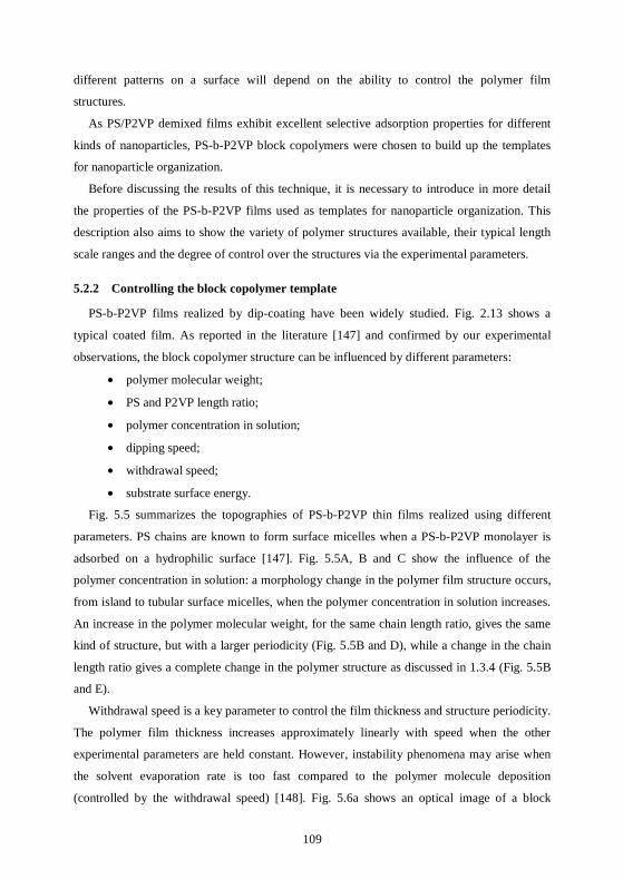
109
different patterns on a surface will depend on the ability to control the polymer film
structures.
As PS/P2VP demixed films exhibit excellent selective adsorption properties for different
kinds of nanoparticles, PS-b-P2VP block copolymers were chosen to build up the templates
for nanoparticle organization.
Before discussing the results of this technique, it is necessary to introduce in more detail
the properties of the PS-b-P2VP films used as templates for nanoparticle organization. This
description also aims to show the variety of polymer structures available, their typical length
scale ranges and the degree of control over the structures via the experimental parameters.
5.2.2 Controlling the block copolymer template
PS-b-P2VP films realized by dip-coating have been widely studied. Fig. 2.13 shows a
typical coated film. As reported in the literature [147] and confirmed by our experimental
observations, the block copolymer structure can be influenced by different parameters:
• polymer molecular weight;
• PS and P2VP length ratio;
• polymer concentration in solution;
• dipping speed;
• withdrawal speed;
• substrate surface energy.
Fig. 5.5 summarizes the topographies of PS-b-P2VP thin films realized using different
parameters. PS chains are known to form surface micelles when a PS-b-P2VP monolayer is
adsorbed on a hydrophilic surface [147]. Fig. 5.5A, B and C show the influence of the
polymer concentration in solution: a morphology change in the polymer film structure occurs,
from island to tubular surface micelles, when the polymer concentration in solution increases.
An increase in the polymer molecular weight, for the same chain length ratio, gives the same
kind of structure, but with a larger periodicity (Fig. 5.5B and D), while a change in the chain
length ratio gives a complete change in the polymer structure as discussed in 1.3.4 (Fig. 5.5B
and E).
Withdrawal speed is a key parameter to control the film thickness and structure periodicity.
The polymer film thickness increases approximately linearly with speed when the other
experimental parameters are held constant. However, instability phenomena may arise when
the solvent evaporation rate is too fast compared to the polymer molecule deposition
(controlled by the withdrawal speed) [148]. Fig. 5.6a shows an optical image of a block
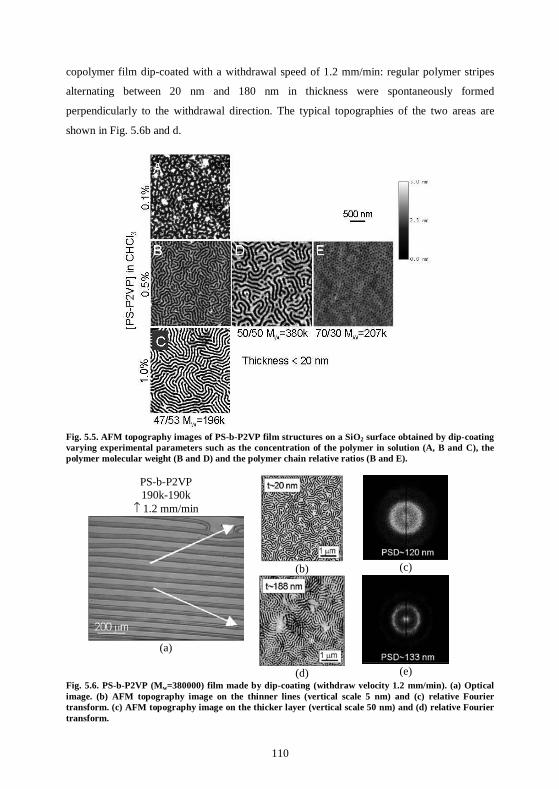
110
copolymer film dip-coated with a withdrawal speed of 1.2 mm/min: regular polymer stripes
alternating between 20 nm and 180 nm in thickness were spontaneously formed
perpendicularly to the withdrawal direction. The typical topographies of the two areas are
shown in Fig. 5.6b and d.
Fig. 5.5. AFM topography images of PS-b-P2VP film structures on a SiO2 surface obtained by dip-coating varying experimental parameters such as the concentration of the polymer in solution (A, B and C), the polymer molecular weight (B and D) and the polymer chain relative ratios (B and E).
PS-b-P2VP 190k-190k
↑ 1.2 mm/min
(b)
(c)
(a)
(d)
(e)
Fig. 5.6. PS-b-P2VP (Mw=380000) film made by dip-coating (withdraw velocity 1.2 mm/min). (a) Optical image. (b) AFM topography image on the thinner lines (vertical scale 5 nm) and (c) relative Fourier transform. (c) AFM topography image on the thicker layer (vertical scale 50 nm) and (d) relative Fourier transform.
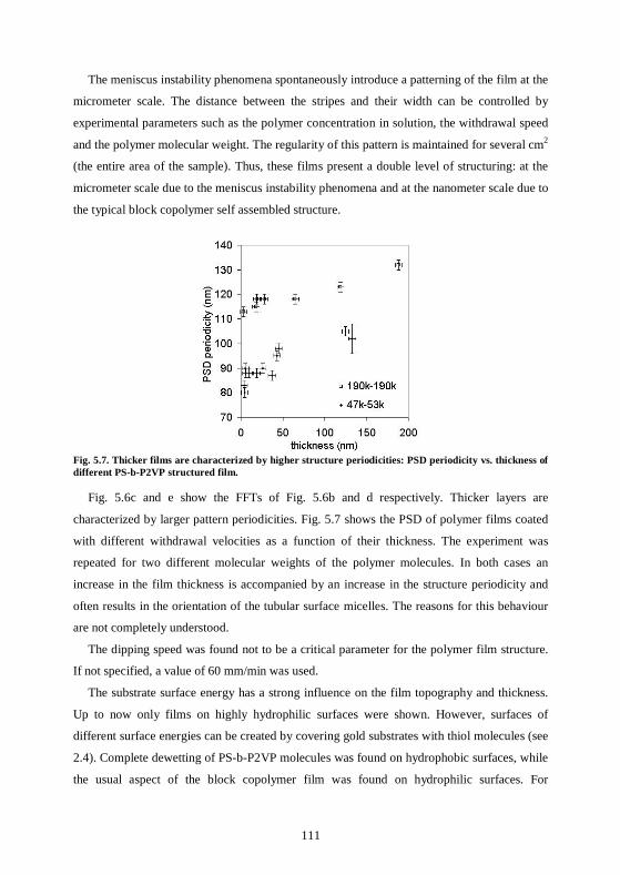
111
The meniscus instability phenomena spontaneously introduce a patterning of the film at the
micrometer scale. The distance between the stripes and their width can be controlled by
experimental parameters such as the polymer concentration in solution, the withdrawal speed
and the polymer molecular weight. The regularity of this pattern is maintained for several cm2
(the entire area of the sample). Thus, these films present a double level of structuring: at the
micrometer scale due to the meniscus instability phenomena and at the nanometer scale due to
the typical block copolymer self assembled structure.
Fig. 5.7. Thicker films are characterized by higher structure periodicities: PSD periodicity vs. thickness of different PS-b-P2VP structured film.
Fig. 5.6c and e show the FFTs of Fig. 5.6b and d respectively. Thicker layers are
characterized by larger pattern periodicities. Fig. 5.7 shows the PSD of polymer films coated
with different withdrawal velocities as a function of their thickness. The experiment was
repeated for two different molecular weights of the polymer molecules. In both cases an
increase in the film thickness is accompanied by an increase in the structure periodicity and
often results in the orientation of the tubular surface micelles. The reasons for this behaviour
are not completely understood.
The dipping speed was found not to be a critical parameter for the polymer film structure.
If not specified, a value of 60 mm/min was used.
The substrate surface energy has a strong influence on the film topography and thickness.
Up to now only films on highly hydrophilic surfaces were shown. However, surfaces of
different surface energies can be created by covering gold substrates with thiol molecules (see
2.4). Complete dewetting of PS-b-P2VP molecules was found on hydrophobic surfaces, while
the usual aspect of the block copolymer film was found on hydrophilic surfaces. For

112
intermediate surface energies an increase of film thickness with substrate hydrophilicity was
observed. An example of such a behaviour is reported in Tab. 5.1.
Thiol solution Film thickness (nm)
Hexadecanethiol 0.5 mM in ethanol Complete dewetting Mixture of
hexadecanethiol/mercaptohexadecanoic acid 50/50 0.5 mM in ethanol
14 ± 2
mercaptohexadecanoic acid 0.5 mM in ethanol
26 ± 2
Tab. 5.1. Thickness of PS-b-P2VP (Mw=380000) films dip-coated (dipping and withdrawal speeds respectively 60 mm/min and 12 mm/min) on gold surfaces previously functionalised via dipping process (1min) in different thiol solutions, rinsed in ethanol and dried under nitrogen.
Micro-contact printing was used to create a pattern of wettability on the gold surfaces.
Block copolymer film were dip-coated these substrates and a double level of the film pattern
was achieved.
(a)
(b)
Fig. 5.8. Influence of the substrate surface energy on the polymer film structure: (a) AFM topography image of a PS-b-P2VP film dip-coated on a gold surface pre-patterned by micro-contact printing and scratched (Mw=380000, 0.5% from chloroform, dipping and withdrawal speeds 60mm/min and 12mm/min, the arrow indicates the withdrawal direction. Vertical scale 100 nm) (b) The same film of the image before in a region patterned with wider hydrophobic stripes (vertical scale 40 nm).
Fig. 5.8a shows the AFM topography image of a PS-b-P2VP film coated on a gold surface
previously patterned with COOH- and CH3-terminated thiols (areas A and B respectively) as
described in 2.5.1. The film was then scratched. A topography similar to that of films coated
on clean Si surfaces was found on the hydrophilic regions. In contrast, a very different
topography was found on hydrophobic regions. Complete dewetting on the hydrophobic
regions was found for large stripe spacing (Fig. 5.8b). It is interesting to observe that an
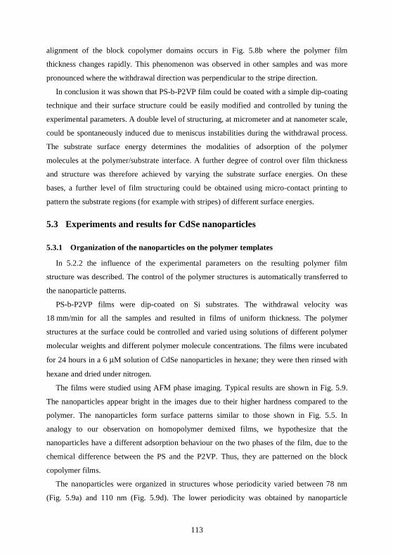
113
alignment of the block copolymer domains occurs in Fig. 5.8b where the polymer film
thickness changes rapidly. This phenomenon was observed in other samples and was more
pronounced where the withdrawal direction was perpendicular to the stripe direction.
In conclusion it was shown that PS-b-P2VP film could be coated with a simple dip-coating
technique and their surface structure could be easily modified and controlled by tuning the
experimental parameters. A double level of structuring, at micrometer and at nanometer scale,
could be spontaneously induced due to meniscus instabilities during the withdrawal process.
The substrate surface energy determines the modalities of adsorption of the polymer
molecules at the polymer/substrate interface. A further degree of control over film thickness
and structure was therefore achieved by varying the substrate surface energies. On these
bases, a further level of film structuring could be obtained using micro-contact printing to
pattern the substrate regions (for example with stripes) of different surface energies.
5.3 Experiments and results for CdSe nanoparticles
5.3.1 Organization of the nanoparticles on the polymer templates
In 5.2.2 the influence of the experimental parameters on the resulting polymer film
structure was described. The control of the polymer structures is automatically transferred to
the nanoparticle patterns.
PS-b-P2VP films were dip-coated on Si substrates. The withdrawal velocity was
18 mm/min for all the samples and resulted in films of uniform thickness. The polymer
structures at the surface could be controlled and varied using solutions of different polymer
molecular weights and different polymer molecule concentrations. The films were incubated
for 24 hours in a 6 µM solution of CdSe nanoparticles in hexane; they were then rinsed with
hexane and dried under nitrogen.
The films were studied using AFM phase imaging. Typical results are shown in Fig. 5.9.
The nanoparticles appear bright in the images due to their higher hardness compared to the
polymer. The nanoparticles form surface patterns similar to those shown in Fig. 5.5. In
analogy to our observation on homopolymer demixed films, we hypothesize that the
nanoparticles have a different adsorption behaviour on the two phases of the film, due to the
chemical difference between the PS and the P2VP. Thus, they are patterned on the block
copolymer films.
The nanoparticles were organized in structures whose periodicity varied between 78 nm
(Fig. 5.9a) and 110 nm (Fig. 5.9d). The lower periodicity was obtained by nanoparticle
114
adsorption on films of polymers with lower molecular weights and concentrations. In contrast,
higher periodicities corresponded to films dip-coated from solutions having higher molecular
weight polymers and concentrations. The nanoparticles were organized in isolated domain
structures (Fig. 5.9a, c and d) or in a continuous holey phase (Fig. 5.9b) depending on the film
structure.
In conclusion, the nanoparticles have a different adsorption behaviour on the two polymer
phases and this allows the nanoparticle patterning on the polymer films. Controlling the
polymer template it is possible to confer to the nanoparticle patterns different periodicities
and shapes.
(a)
(b)
(c)
(d)
Fig. 5.9. AFM phase images (2µm × 2µm) of CdSe nanoparticles organized in different structures. Polymer substrates: PS-b-P2VP dip-coated at 18 mm/min; (a) Mw=196000; 0.5% from chloroform. (b) Mw=196000; 1.0% from chloroform. (c) Mw=380000; 0.5% from chloroform. (a) Mw=380000; 1.0% from chloroform. Substrates dipped 24 hours in a solution of CdSe nanoparticles 6 µM in hexane.
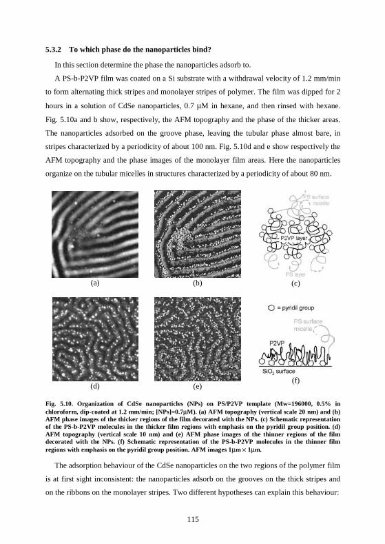
115
5.3.2 To which phase do the nanoparticles bind?
In this section determine the phase the nanoparticles adsorb to.
A PS-b-P2VP film was coated on a Si substrate with a withdrawal velocity of 1.2 mm/min
to form alternating thick stripes and monolayer stripes of polymer. The film was dipped for 2
hours in a solution of CdSe nanoparticles, 0.7 µM in hexane, and then rinsed with hexane.
Fig. 5.10a and b show, respectively, the AFM topography and the phase of the thicker areas.
The nanoparticles adsorbed on the groove phase, leaving the tubular phase almost bare, in
stripes characterized by a periodicity of about 100 nm. Fig. 5.10d and e show respectively the
AFM topography and the phase images of the monolayer film areas. Here the nanoparticles
organize on the tubular micelles in structures characterized by a periodicity of about 80 nm.
(a)
(b)
(c)
(d)
(e)
(f)
Fig. 5.10. Organization of CdSe nanoparticles (NPs) on PS/P2VP template (Mw=196000, 0.5% in chloroform, dip-coated at 1.2 mm/min; [NPs]=0.7µM). (a) AFM topography (vertical scale 20 nm) and (b) AFM phase images of the thicker regions of the film decorated with the NPs. (c) Schematic representation of the PS-b-P2VP molecules in the thicker film regions with emphasis on the pyridil group position. (d) AFM topography (vertical scale 10 nm) and (e) AFM phase images of the thinner regions of the film decorated with the NPs. (f) Schematic representation of the PS-b-P2VP molecules in the thinner film regions with emphasis on the pyridil group position. AFM images 1µm × 1µm.
The adsorption behaviour of the CdSe nanoparticles on the two regions of the polymer film
is at first sight inconsistent: the nanoparticles adsorb on the grooves on the thick stripes and
on the ribbons on the monolayer stripes. Two different hypotheses can explain this behaviour:
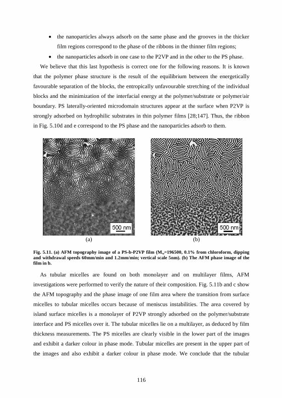
116
• the nanoparticles always adsorb on the same phase and the grooves in the thicker
film regions correspond to the phase of the ribbons in the thinner film regions;
• the nanoparticles adsorb in one case to the P2VP and in the other to the PS phase.
We believe that this last hypothesis is correct one for the following reasons. It is known
that the polymer phase structure is the result of the equilibrium between the energetically
favourable separation of the blocks, the entropically unfavourable stretching of the individual
blocks and the minimization of the interfacial energy at the polymer/substrate or polymer/air
boundary. PS laterally-oriented microdomain structures appear at the surface when P2VP is
strongly adsorbed on hydrophilic substrates in thin polymer films [28;147]. Thus, the ribbon
in Fig. 5.10d and e correspond to the PS phase and the nanoparticles adsorb to them.
(a)
(b)
Fig. 5.11. (a) AFM topography image of a PS-b-P2VP film (Mw=196500, 0.1% from chloroform, dipping and withdrawal speeds 60mm/min and 1.2mm/min; vertical scale 5nm). (b) The AFM phase image of the film in b.
As tubular micelles are found on both monolayer and on multilayer films, AFM
investigations were performed to verify the nature of their composition. Fig. 5.11b and c show
the AFM topography and the phase image of one film area where the transition from surface
micelles to tubular micelles occurs because of meniscus instabilities. The area covered by
island surface micelles is a monolayer of P2VP strongly adsorbed on the polymer/substrate
interface and PS micelles over it. The tubular micelles lie on a multilayer, as deduced by film
thickness measurements. The PS micelles are clearly visible in the lower part of the images
and exhibit a darker colour in phase mode. Tubular micelles are present in the upper part of
the images and also exhibit a darker colour in phase mode. We conclude that the tubular
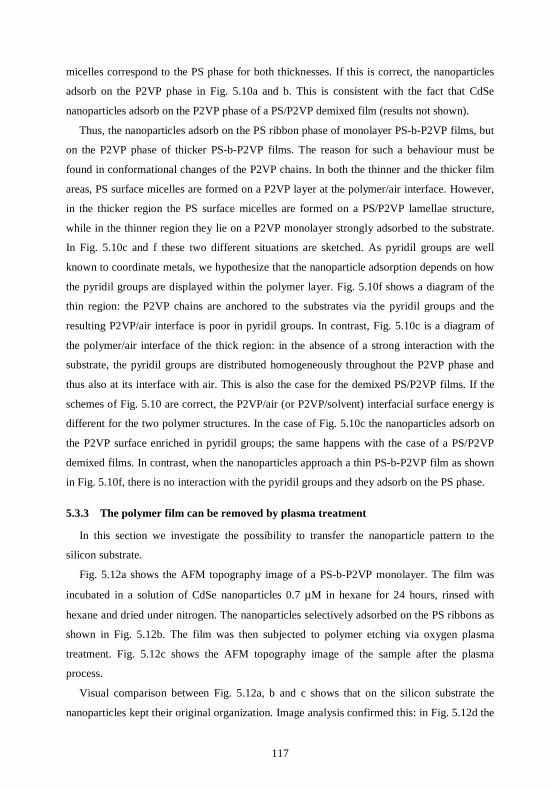
117
micelles correspond to the PS phase for both thicknesses. If this is correct, the nanoparticles
adsorb on the P2VP phase in Fig. 5.10a and b. This is consistent with the fact that CdSe
nanoparticles adsorb on the P2VP phase of a PS/P2VP demixed film (results not shown).
Thus, the nanoparticles adsorb on the PS ribbon phase of monolayer PS-b-P2VP films, but
on the P2VP phase of thicker PS-b-P2VP films. The reason for such a behaviour must be
found in conformational changes of the P2VP chains. In both the thinner and the thicker film
areas, PS surface micelles are formed on a P2VP layer at the polymer/air interface. However,
in the thicker region the PS surface micelles are formed on a PS/P2VP lamellae structure,
while in the thinner region they lie on a P2VP monolayer strongly adsorbed to the substrate.
In Fig. 5.10c and f these two different situations are sketched. As pyridil groups are well
known to coordinate metals, we hypothesize that the nanoparticle adsorption depends on how
the pyridil groups are displayed within the polymer layer. Fig. 5.10f shows a diagram of the
thin region: the P2VP chains are anchored to the substrates via the pyridil groups and the
resulting P2VP/air interface is poor in pyridil groups. In contrast, Fig. 5.10c is a diagram of
the polymer/air interface of the thick region: in the absence of a strong interaction with the
substrate, the pyridil groups are distributed homogeneously throughout the P2VP phase and
thus also at its interface with air. This is also the case for the demixed PS/P2VP films. If the
schemes of Fig. 5.10 are correct, the P2VP/air (or P2VP/solvent) interfacial surface energy is
different for the two polymer structures. In the case of Fig. 5.10c the nanoparticles adsorb on
the P2VP surface enriched in pyridil groups; the same happens with the case of a PS/P2VP
demixed films. In contrast, when the nanoparticles approach a thin PS-b-P2VP film as shown
in Fig. 5.10f, there is no interaction with the pyridil groups and they adsorb on the PS phase.
5.3.3 The polymer film can be removed by plasma treatment
In this section we investigate the possibility to transfer the nanoparticle pattern to the
silicon substrate.
Fig. 5.12a shows the AFM topography image of a PS-b-P2VP monolayer. The film was
incubated in a solution of CdSe nanoparticles 0.7 µM in hexane for 24 hours, rinsed with
hexane and dried under nitrogen. The nanoparticles selectively adsorbed on the PS ribbons as
shown in Fig. 5.12b. The film was then subjected to polymer etching via oxygen plasma
treatment. Fig. 5.12c shows the AFM topography image of the sample after the plasma
process.
Visual comparison between Fig. 5.12a, b and c shows that on the silicon substrate the
nanoparticles kept their original organization. Image analysis confirmed this: in Fig. 5.12d the
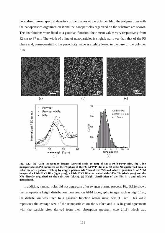
118
normalized power spectral densities of the images of the polymer film, the polymer film with
the nanoparticles organized on it and the nanoparticles organized on the substrate are shown.
The distributions were fitted to a gaussian function: their mean values vary respectively from
82 nm to 87 nm. The width of a line of nanoparticles is slightly narrower than that of the PS
phase and, consequentially, the periodicity value is slightly lower in the case of the polymer
film.
(a)
(b)
(c)
(d)
(e)
Fig. 5.12. (a) AFM topography images (vertical scale 10 nm) of (a) a PS-b-P2VP film. (b) CdSe nanoparticles (NPs) organized on the PS phase of the PS-b.P2VP film in a. (c) CdSe NPs patterned on a Si substrate after polymer etching by oxygen plasma. (d) Normalized PSD and relative gaussian fit of AFM images of a PS-b-P2VP film (light grey), a PS-b-P2VP film decorated with CdSe NPs (dark grey) and the NPs directly organized on the substrate (black). (e) Height distribution of the NPs in c and relative gaussian fit.
In addition, nanoparticles did not aggregate after oxygen plasma process. Fig. 5.12e shows
the nanoparticle height distribution measured on AFM topography images such as Fig. 5.12c;
the distribution was fitted to a gaussian function whose mean was 3.6 nm. This value
represents the average size of the nanoparticles on the surface and it is in good agreement
with the particle sizes derived from their absorption spectrum (see 2.1.1) which was
119
approximately 3.5 nm. The asymmetry of the distribution in Fig. 5.12e is due to the image
processing procedure. In addition, a peak around 11 nm is visible in Fig. 5.12d that is due to
nanoparticle aggregation and residual polymer on the surface.
Fig. 5.12 shows the result for nanoparticles originally distributed on a polymer monolayer.
The same experiment was performed using thicker PS-b-P2VP layer. Removal of these
polymer layers requires longer etching (longer than 3 min). As far as the measurements
performed in this work are concerned, the organization of the nanoparticles originally
adsorbed on thick polymer films was lost during the etching.
5.4 Experiments and results for gold nanoparticles
5.4.1 Organization of gold nanoparticles on polymer templates
Gold nanoparticles of 20 nm and 10 nm in diameter were organized on PS-b-P2VP films
with the same technique described in the previous sections and with similar results as shown
for the CdSe nanoparticles. The possibility to observe gold nanoparticle distribution with
SEM makes them particularly suitable for investigation of their organization on large areas.
The gold nanoparticles and the gold substrate appear bright in the SEM images, while the bare
polymer appears dark.
PS-b-P2VP films were prepared on SiO2 and Cr surfaces as described in 5.2.2. The coating
parameters were controlled in order to obtained templates for the nanoparticle organization
presenting different patterns and length scales. The polymer templates were incubated in
1.3 × 10¹¹ 20 nm Au nanoparticle or, alternatively, in 1.7 × 10¹² 10 nm Au nanoparticle
aqueous solutions for some hours. The samples were then rinsed with water and dried under
nitrogen. The substrates were then observed using SEM.
The nanoparticles selectively adsorbed to one phase of the block copolymer film and result
patterned reproducing the polymer template. Fig. 5.13a shows 10 nm Au nanoparticles
adsorbed to a PS-b-P2VP film dip-coated on a Cr substrate. They are organized in stochastic
patterns. Fig. 5.13b shows, in stead, the same nanoparticles organized in highly ordered
patterns. The nanoparticles were organized in ∼70 nm wide and ∼7 µm long quasi-parallel
lines over tens of µm2. The polymer template was prepared by dip-coating PS-b-P2VP
molecules on a Si substrate from a 0.1% solution of polymer in chloroform with a dipping
speed of 30 mm/min and a withdrawal speed of 0.6 mm/min. Then the substrate was
incubated in the Au nanoparticle solution for some hours, rinsed with water and dried under
nitrogen.
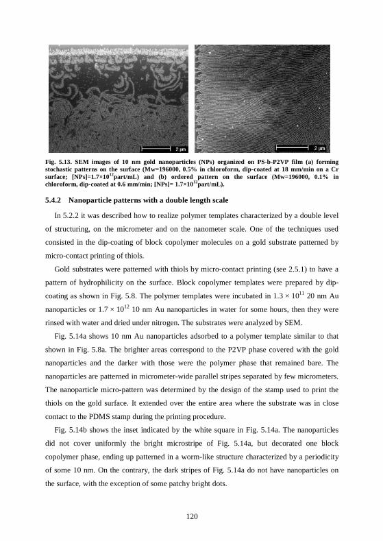
120
Fig. 5.13. SEM images of 10 nm gold nanoparticles (NPs) organized on PS-b-P2VP film (a) forming stochastic patterns on the surface (Mw=196000, 0.5% in chloroform, dip-coated at 18 mm/min on a Cr surface; [NPs]=1.7×10¹²part/mL) and (b) ordered pattern on the surface (Mw=196000, 0.1% in chloroform, dip-coated at 0.6 mm/min; [NPs]= 1.7×10¹²part/mL).
5.4.2 Nanoparticle patterns with a double length scale
In 5.2.2 it was described how to realize polymer templates characterized by a double level
of structuring, on the micrometer and on the nanometer scale. One of the techniques used
consisted in the dip-coating of block copolymer molecules on a gold substrate patterned by
micro-contact printing of thiols.
Gold substrates were patterned with thiols by micro-contact printing (see 2.5.1) to have a
pattern of hydrophilicity on the surface. Block copolymer templates were prepared by dip-
coating as shown in Fig. 5.8. The polymer templates were incubated in 1.3 × 10¹¹ 20 nm Au
nanoparticles or 1.7 × 10¹² 10 nm Au nanoparticles in water for some hours, then they were
rinsed with water and dried under nitrogen. The substrates were analyzed by SEM.
Fig. 5.14a shows 10 nm Au nanoparticles adsorbed to a polymer template similar to that
shown in Fig. 5.8a. The brighter areas correspond to the P2VP phase covered with the gold
nanoparticles and the darker with those were the polymer phase that remained bare. The
nanoparticles are patterned in micrometer-wide parallel stripes separated by few micrometers.
The nanoparticle micro-pattern was determined by the design of the stamp used to print the
thiols on the gold surface. It extended over the entire area where the substrate was in close
contact to the PDMS stamp during the printing procedure.
Fig. 5.14b shows the inset indicated by the white square in Fig. 5.14a. The nanoparticles
did not cover uniformly the bright microstripe of Fig. 5.14a, but decorated one block
copolymer phase, ending up patterned in a worm-like structure characterized by a periodicity
of some 10 nm. On the contrary, the dark stripes of Fig. 5.14a do not have nanoparticles on
the surface, with the exception of some patchy bright dots.
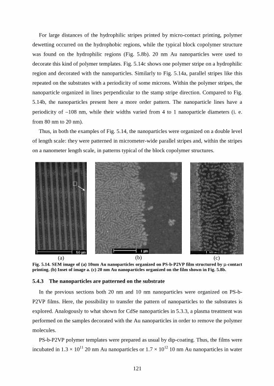
121
For large distances of the hydrophilic stripes printed by micro-contact printing, polymer
dewetting occurred on the hydrophobic regions, while the typical block copolymer structure
was found on the hydrophilic regions (Fig. 5.8b). 20 nm Au nanoparticles were used to
decorate this kind of polymer templates. Fig. 5.14c shows one polymer stripe on a hydrophilic
region and decorated with the nanoparticles. Similarly to Fig. 5.14a, parallel stripes like this
repeated on the substrates with a periodicity of some microns. Within the polymer stripes, the
nanoparticle organized in lines perpendicular to the stamp stripe direction. Compared to Fig.
5.14b, the nanoparticles present here a more order pattern. The nanoparticle lines have a
periodicity of ∼108 nm, while their widths varied from 4 to 1 nanoparticle diameters (i. e.
from 80 nm to 20 nm).
Thus, in both the examples of Fig. 5.14, the nanoparticles were organized on a double level
of length scale: they were patterned in micrometer-wide parallel stripes and, within the stripes
on a nanometer length scale, in patterns typical of the block copolymer structures.
(a)
(b)
(c)
Fig. 5.14. SEM image of (a) 10nm Au nanoparticles organized on PS-b-P2VP film structured by µ-contact printing. (b) Inset of image a. (c) 20 nm Au nanoparticles organized on the film shown in Fig. 5.8b.
5.4.3 The nanoparticles are patterned on the substrate
In the previous sections both 20 nm and 10 nm nanoparticles were organized on PS-b-
P2VP films. Here, the possibility to transfer the pattern of nanoparticles to the substrates is
explored. Analogously to what shown for CdSe nanoparticles in 5.3.3, a plasma treatment was
performed on the samples decorated with the Au nanoparticles in order to remove the polymer
molecules.
PS-b-P2VP polymer templates were prepared as usual by dip-coating. Thus, the films were
incubated in 1.3 × 10¹¹ 20 nm Au nanoparticles or 1.7 × 10¹² 10 nm Au nanoparticles in water
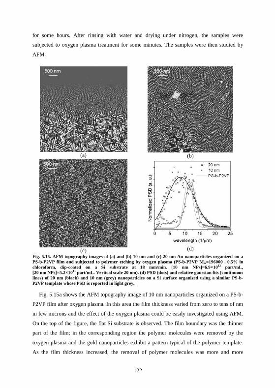
122
for some hours. After rinsing with water and drying under nitrogen, the samples were
subjected to oxygen plasma treatment for some minutes. The samples were then studied by
AFM.
(a)
(b)
(c)
(d)
Fig. 5.15. AFM topography images of (a) and (b) 10 nm and (c) 20 nm Au nanoparticles organized on a PS-b-P2VP film and subjected to polymer etching by oxygen plasma (PS-b-P2VP Mw=196000 , 0.5% in chloroform, dip-coated on a Si substrate at 18 mm/min. [10 nm NPs]=6.9×10¹² part/mL, [20 nm NPs]=5.2×10¹¹ part/mL. Vertical scale 20 nm). (d) PSD (dots) and relative gaussian fits (continuous lines) of 20 nm (black) and 10 nm (grey) nanoparticles on a Si surface organized using a similar PS-b-P2VP template whose PSD is reported in light grey.
Fig. 5.15a shows the AFM topography image of 10 nm nanoparticles organized on a PS-b-
P2VP film after oxygen plasma. In this area the film thickness varied from zero to tens of nm
in few microns and the effect of the oxygen plasma could be easily investigated using AFM.
On the top of the figure, the flat Si substrate is observed. The film boundary was the thinner
part of the film; in the corresponding region the polymer molecules were removed by the
oxygen plasma and the gold nanoparticles exhibit a pattern typical of the polymer template.
As the film thickness increased, the removal of polymer molecules was more and more
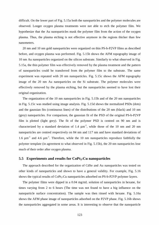
123
difficult. On the lower part of Fig. 5.15a both the nanoparticles and the polymer molecules are
observed. Longer oxygen plasma treatments were not able to etch the polymer film. We
hypothesize that the Au nanoparticles mask the polymer film from the action of the oxygen
plasma. Thus, the plasma etching is not effective anymore in the regions thicker than few
nanometers.
20 nm and 10 nm gold nanoparticles were organized on thin PS-b-P2VP films as described
before, and oxygen plasma was performed. Fig. 5.15b shows the AFM topography image of
10 nm Au nanoparticles organized on the silicon substrate. Similarly to what observed in Fig.
5.15a, the thin polymer film was effectively removed by the plasma treatment and the pattern
of nanoparticles could be transferred from the polymer film to the substrate. The same
experiment was repeated with 20 nm nanoparticles. Fig. 5.15c shows the AFM topography
image of the 20 nm Au nanoparticles on the Si substrate. The polymer molecules were
effectively removed by the plasma etching, but the nanoparticles seemed to have lost their
original organization.
The organization of the 10 nm nanoparticles in Fig. 5.15b and of the 20 nm nanoparticles
in Fig. 5.15c was studied using image analysis. Fig. 5.15d shows the normalized PSDs (dots)
and the gaussian fits (continuous lines) of the distributions of the 20 nm (black) and 10 nm
(grey) nanoparticles. For comparison, the gaussian fit of the PSD of the original PS-b-P2VP
film is plotted (light grey). The fit of the polymer PSD is centred on 90 nm and is
characterized by a standard deviation of 1.4 µm-1, while those of the 10 nm and 20 nm
nanoparticles are centred respectively on 84 nm and 117 nm and have standard deviations of
1.6 µm-1 and 4.6 µm-1. Therefore, while the 10 nm nanoparticles reproduce faithfully the
polymer template (in agreement to what observed in Fig. 5.15b), the 20 nm nanoparticles lose
much of their order after oxygen plasma.
5.5 Experiments and results for CoPt3:Cu nanoparticles
The approach described for the organization of CdSe and Au nanoparticles was tested on
other kinds of nanoparticles and shown to have a general validity. For example, Fig. 5.16
shows the typical results of CoPt3:Cu nanoparticles adsorbed on PS-b-P2VP polymer layers.
The polymer films were dipped in a 0.04 mg/mL solution of nanoparticles in hexane, for
times varying from 2 to 6 hours (The time was not found to have a big influence on the
nanoparticle surface concentration). The sample was then rinsed with hexane. Fig. 5.16a
shows the AFM phase image of nanoparticles adsorbed on the P2VP phase. Fig. 5.16b shows
the nanoparticles aggregated in some areas. It is interesting to observe that the nanoparticle
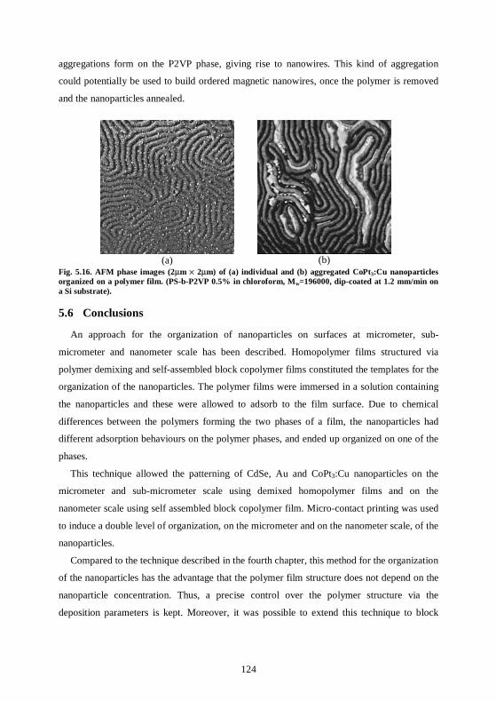
124
aggregations form on the P2VP phase, giving rise to nanowires. This kind of aggregation
could potentially be used to build ordered magnetic nanowires, once the polymer is removed
and the nanoparticles annealed.
(a)
(b)
Fig. 5.16. AFM phase images (2µm × 2µm) of (a) individual and (b) aggregated CoPt3:Cu nanoparticles organized on a polymer film. (PS-b-P2VP 0.5% in chloroform, Mw=196000, dip-coated at 1.2 mm/min on a Si substrate).
5.6 Conclusions
An approach for the organization of nanoparticles on surfaces at micrometer, sub-
micrometer and nanometer scale has been described. Homopolymer films structured via
polymer demixing and self-assembled block copolymer films constituted the templates for the
organization of the nanoparticles. The polymer films were immersed in a solution containing
the nanoparticles and these were allowed to adsorb to the film surface. Due to chemical
differences between the polymers forming the two phases of a film, the nanoparticles had
different adsorption behaviours on the polymer phases, and ended up organized on one of the
phases.
This technique allowed the patterning of CdSe, Au and CoPt3:Cu nanoparticles on the
micrometer and sub-micrometer scale using demixed homopolymer films and on the
nanometer scale using self assembled block copolymer film. Micro-contact printing was used
to induce a double level of organization, on the micrometer and on the nanometer scale, of the
nanoparticles.
Compared to the technique described in the fourth chapter, this method for the organization
of the nanoparticles has the advantage that the polymer film structure does not depend on the
nanoparticle concentration. Thus, a precise control over the polymer structure via the
deposition parameters is kept. Moreover, it was possible to extend this technique to block
125
copolymer templates and thus to reduce the nanoparticle pattern periodicities to the tens of
nanometer scale.
Zehner et al. [89] also reported on the selective decoration of a phase separated PS-b-
PMMA block copolymer film with thiol passivated gold nanocrystals. However, their study
was limited to this specific system. In this work we demonstrate the general validity of the
approach for the organization of the nanoparticles. In the same work, they observed a
dependency in the polymer surface covering on the nanoparticle concentration in solution. We
observed the same phenomenon and we could demonstrate that under certain conditions the
nanoparticles do not aggregate either before or after the action of the oxygen plasma.
In addition, using the same technique we could transfer the nanoparticle patterns to a hard
surface. The organic molecules of thin block copolymer film were removed by an oxygen
plasma leaving the nanoparticles organized on the substrate. Good reproducibility of the
polymer patterns was found for 10 nm Au nanoparticles and CdSe nanoparticles, while the for
the 20 nm Au nanoparticles some of the order was lost on plasma etching. Particle analysis
demonstrated that under certain conditions the technique prevented nanoparticle aggregation.
The experiments described were performed on Au, Si and Cr surfaces. However, this
technique can be extended to any kind of substrate suitable for polymer dip-coating,
irrespective of its material and shape, as long as it is resistant to oxygen plasma. Thus, this
technique allows the patterning of different kinds of inorganic nanoparticles on metal or
semiconductor substrates.

127
Chapter 6
6 Conductive nanostructures
This chapter concerns the creation of gold nanostructures and nanowires. Block copolymer
films were used as templates and the nanoparticles were organized on them. Aggregation
between the nanoparticles was induced for the formation of continuous structures. The
conductivity of the gold nanostructures was demonstrated using SEM.
6.1 Au nanoparticles on a thick polymer layer remain electrically
insulated from the substrate
20 nm and 10 nm Au nanoparticles were organized as described in 5.4 on PS-b-P2VP film.
An oxygen plasma was applied to remove the polymer molecules. The oxygen plasma was
effective for thin polymer film removal and the nanoparticles ended up in contact with the Si
substrate. In contrast, nanoparticles on thick polymer layers masked the film from the etching
and the polymer was only partly removed (Fig. 5.15a).
The electrical isolation of the gold nanoparticles from the substrate was verified using
SEM. As described in 2.2.5, SEM makes use of an electron beam to scan the sample surface
and generate secondary scattered electrons which are detected. The beam electrons are then
dispersed via the substrate. If the substrate is not in good electrical contact with the sample,
part of the beam electrons remain confined in the sample metal structures. The increased
electron density induces a higher probability of scattered electrons and thus a higher detected
signal. As a consequence, the sample area with a higher electron density appears brighter
compared to the rest of the sample (charging effect).
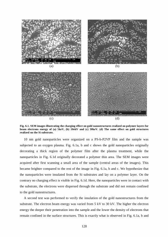
128
(a)
(b)
(c)
(d)
Fig. 6.1. SEM images illustrating the charging effect on gold nanostructures realized on polymer layers for beam electrons energy of (a) 5keV, (b) 10ekV and (c) 30keV. (d) The same effect on gold structures realized on the Si substrate.
10 nm gold nanoparticles were organized on a PS-b-P2VP film and the sample was
subjected to an oxygen plasma. Fig. 6.1a, b and c shows the gold nanoparticles originally
decorating a thick region of the polymer film after the plasma treatment, while the
nanoparticles in Fig. 6.1d originally decorated a polymer thin area. The SEM images were
acquired after first scanning a small area of the sample (central areas of the images). This
became brighter compared to the rest of the image in Fig. 6.1a, b and c. We hypothesize that
the nanoparticles were insulated from the Si substrates and lay on a polymer layer. On the
contrary no charging effect is visible in Fig. 6.1d. Here, the nanoparticles were in contact with
the substrate, the electrons were dispersed through the substrate and did not remain confined
to the gold nanostructures.
A second test was performed to verify the insulation of the gold nanostructures from the
substrate. The electron beam energy was varied from 5 kV to 30 kV. The higher the electron
energy the deeper their penetration into the sample and the lower the density of electrons that
remain confined in the surface structures. This is exactly what is observed in Fig. 6.1a, b and
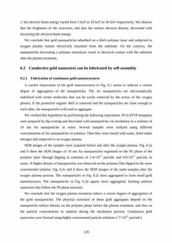
129
c: the electron beam energy varied from 5 keV to 10 keV to 30 keV respectively. We observe
that the brightness of the structures, and thus the surface electron density, decreased with
increasing the electron beam energy.
We conclude that gold nanoparticles adsorbed on a thick polymer layer and subjected to
oxygen plasma remain electrically insulated from the substrate. On the contrary, the
nanoparticles decorating a polymer monolayer result in electrical contact with the substrate
after the plasma treatment.
6.2 Conductive gold nanowires can be fabricated by self-assembly
6.2.1 Fabrication of continuous gold nanostructures
A careful observation of the gold nanostructures in Fig. 6.1 seems to indicate a certain
degree of aggregation of the nanoparticles. The Au nanoparticles are electrostatically
stabilized with citrate molecules that can be easily removed by the action of the oxygen
plasma. If the protective organic shell is removed and the nanoparticles are close enough to
each other, the nanoparticles will tend to aggregate.
We verified this hypothesis by performing the following experiment. PS-b-P2VP templates
were prepared by dip-coating and decorated with nanoparticles via incubation in a solution of
10 nm Au nanoparticles in water. Several samples were realized using different
concentrations of Au nanoparticles in solution. Then they were rinsed with water, dried under
nitrogen and subjected to an oxygen plasma.
SEM images of the samples were acquired before and after the oxygen plasma. Fig. 6.2a
and b show the SEM images of 10 nm Au nanoparticles organized on the PS phase of the
polymer layer through dipping in solutions of 1.4×10¹¹ part/mL and 6.9×10¹¹ part/mL in
water. A higher density of nanoparticles was observed on the polymer film dipped in the more
concentrated solution. Fig. 6.2c and d show the SEM images of the same samples after the
oxygen plasma process. The nanoparticles in Fig. 6.2c have aggregated to form small gold
nanostructures. The nanoparticles in Fig. 6.2d appear more aggregated, forming uniform
nanowires that follow the PS phase structure.
We conclude that the oxygen plasma treatment induce a certain degree of aggregation of
the gold nanoparticles. The physical extension of these gold aggregates depend on the
nanoparticle surface density on the polymer phase before the plasma treatment, and thus on
the particle concentration in solution during the incubation process. Continuous gold
nanowires were formed using highly concentrated particle solutions (~7×10¹¹ part/mL).
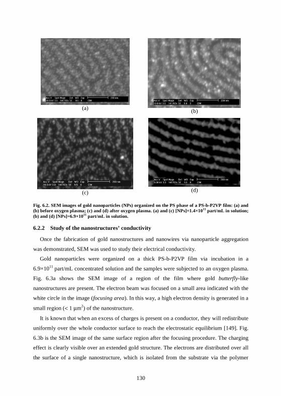
130
(a)
(b)
(c)
(d)
Fig. 6.2. SEM images of gold nanoparticles (NPs) organized on the PS phase of a PS-b-P2VP film: (a) and (b) before oxygen plasma; (c) and (d) after oxygen plasma. (a) and (c) [NPs]=1.4×10¹¹ part/mL in solution; (b) and (d) [NPs]=6.9×10¹¹ part/mL in solution.
6.2.2 Study of the nanostructures’ conductivity
Once the fabrication of gold nanostructures and nanowires via nanoparticle aggregation
was demonstrated, SEM was used to study their electrical conductivity.
Gold nanoparticles were organized on a thick PS-b-P2VP film via incubation in a
6.9×10¹¹ part/mL concentrated solution and the samples were subjected to an oxygen plasma.
Fig. 6.3a shows the SEM image of a region of the film where gold butterfly-like
nanostructures are present. The electron beam was focused on a small area indicated with the
white circle in the image (focusing area). In this way, a high electron density is generated in a
small region (< 1 µm2) of the nanostructure.
It is known that when an excess of charges is present on a conductor, they will redistribute
uniformly over the whole conductor surface to reach the electrostatic equilibrium [149]. Fig.
6.3b is the SEM image of the same surface region after the focusing procedure. The charging
effect is clearly visible over an extended gold structure. The electrons are distributed over all
the surface of a single nanostructure, which is isolated from the substrate via the polymer
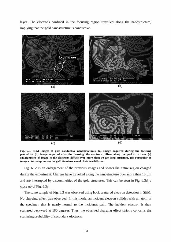
131
layer. The electrons confined in the focusing region travelled along the nanostructure,
implying that the gold nanostructure is conductive.
(a)
(b)
(c)
(d)
Fig. 6.3. SEM images of gold conductive nanostructures. (a) Image acquired during the focusing procedure. (b) Image acquired after the focusing: the electrons diffuse along the gold structures. (c) Enlargement of image c: the electrons diffuse over more than 10 µm long structure. (d) Particular of image c: interruptions in the gold structure avoid electrons diffusion.
Fig. 6.3c is an enlargement of the previous images and shows the entire region charged
during the experiment. Charges have travelled along the nanostructure over more than 10 µm
and are interrupted by discontinuities of the gold structures. This can be seen in Fig. 6.3d, a
close up of Fig. 6.3c.
The same sample of Fig. 6.3 was observed using back scattered electron detection in SEM.
No charging effect was observed. In this mode, an incident electron collides with an atom in
the specimen that is nearly normal to the incident's path. The incident electron is then
scattered backward at 180 degrees. Thus, the observed charging effect strictly concerns the
scattering probability of secondary electrons.
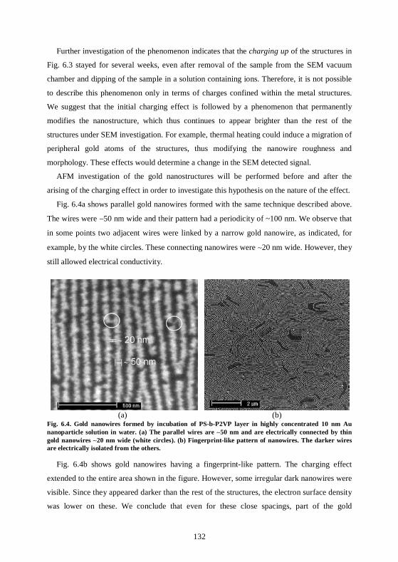
132
Further investigation of the phenomenon indicates that the charging up of the structures in
Fig. 6.3 stayed for several weeks, even after removal of the sample from the SEM vacuum
chamber and dipping of the sample in a solution containing ions. Therefore, it is not possible
to describe this phenomenon only in terms of charges confined within the metal structures.
We suggest that the initial charging effect is followed by a phenomenon that permanently
modifies the nanostructure, which thus continues to appear brighter than the rest of the
structures under SEM investigation. For example, thermal heating could induce a migration of
peripheral gold atoms of the structures, thus modifying the nanowire roughness and
morphology. These effects would determine a change in the SEM detected signal.
AFM investigation of the gold nanostructures will be performed before and after the
arising of the charging effect in order to investigate this hypothesis on the nature of the effect.
Fig. 6.4a shows parallel gold nanowires formed with the same technique described above.
The wires were ∼50 nm wide and their pattern had a periodicity of ~100 nm. We observe that
in some points two adjacent wires were linked by a narrow gold nanowire, as indicated, for
example, by the white circles. These connecting nanowires were ∼20 nm wide. However, they
still allowed electrical conductivity.
(a)
(b)
Fig. 6.4. Gold nanowires formed by incubation of PS-b-P2VP layer in highly concentrated 10 nm Au nanoparticle solution in water. (a) The parallel wires are ∼50 nm and are electrically connected by thin gold nanowires ∼20 nm wide (white circles). (b) Fingerprint-like pattern of nanowires. The darker wires are electrically isolated from the others.
Fig. 6.4b shows gold nanowires having a fingerprint-like pattern. The charging effect
extended to the entire area shown in the figure. However, some irregular dark nanowires were
visible. Since they appeared darker than the rest of the structures, the electron surface density
was lower on these. We conclude that even for these close spacings, part of the gold
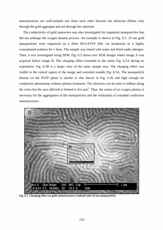
133
nanostructures are well-isolated one from each other because the electrons diffuse only
through the gold aggregate and not through the substrate.
The conductivity of gold nanowires was also investigated for organized nanoparticles that
did not undergo the oxygen plasma process. An example is shown in Fig. 6.5. 10 nm gold
nanoparticles were organized on a thick PS-b-P2VP film via incubation in a highly
concentrated solution for 1 hour. The sample was rinsed with water and dried under nitrogen.
Then, it was investigated using SEM. Fig. 6.5 shows two SEM images where image A was
acquired before image B. The charging effect extended to the entire Fig. 6.5A during its
acquisition. Fig. 6.5B is a larger view of the same sample area. The charging effect was
visible in the central region of the image and extended outside Fig. 6.5A. The nanoparticle
density on the P2VP phase is similar to that shown in Fig. 6.2b and high enough for
conductive phenomena without plasma treatment. The electrons can be seen to diffuse along
the wires but the area affected is limited to few µm2. Thus, the action of an oxygen plasma is
necessary for the aggregation of the nanoparticles and the realization of extended conductive
nanostructures.
Fig. 6.5. Charging effect on gold nanostructures realized with 10 nm nanoparticles
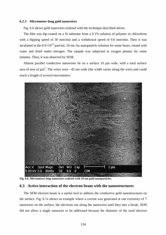
134
6.2.3 Micrometer-long gold nanowires
Fig. 6.6 shows gold nanowires realized with the technique described above.
The film was dip-coated on a Si substrate from a 0.1% solution of polymer in chloroform
with a dipping speed of 30 mm/min and a withdrawal speed of 0.6 mm/min. Then it was
incubated in the 6.9×10¹² part/mL 10 nm Au nanoparticle solution for some hours, rinsed with
water and dried under nitrogen. The sample was subjected to oxygen plasma for some
minutes. Then, it was observed by SEM.
Almost parallel conductive nanowires lie on a surface 10 µm wide, with a total surface
area of tens of µm2. The wires were ∼45 nm wide (the width varies along the wire) and could
reach a length of several micrometers.
Fig. 6.6. Micrometers long nanowires realized with 10 nm gold nanoparticles.
6.3 Active interaction of the electron beam with the nanostructures
The SEM electron beam is a useful tool to address the conductive gold nanostructures on
the surface. Fig. 6.7a shows an example where a current was generated at one extremity of 7
nanowires on the surface; the electrons ran along the nanowires until they met a break. SEM
did not allow a single nanowire to be addressed because the diameter of the used electron
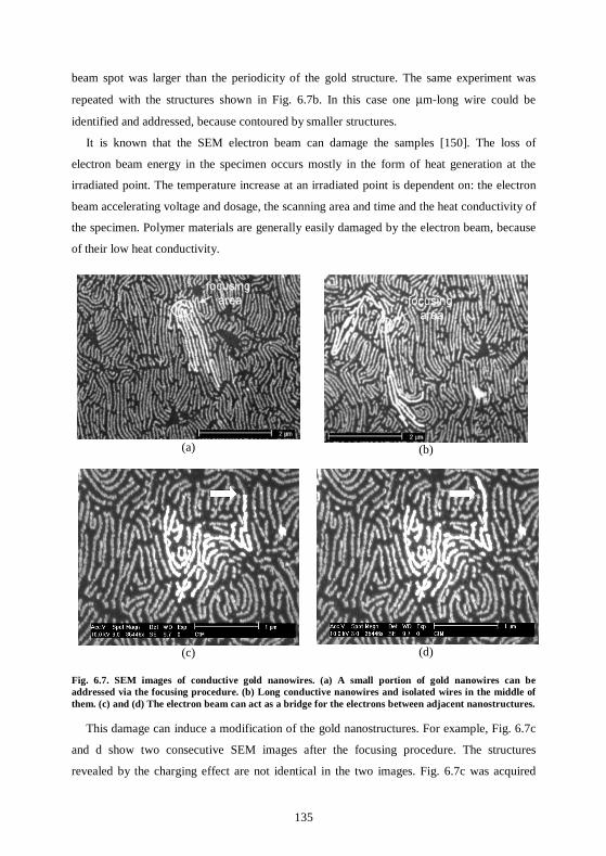
135
beam spot was larger than the periodicity of the gold structure. The same experiment was
repeated with the structures shown in Fig. 6.7b. In this case one µm-long wire could be
identified and addressed, because contoured by smaller structures.
It is known that the SEM electron beam can damage the samples [150]. The loss of
electron beam energy in the specimen occurs mostly in the form of heat generation at the
irradiated point. The temperature increase at an irradiated point is dependent on: the electron
beam accelerating voltage and dosage, the scanning area and time and the heat conductivity of
the specimen. Polymer materials are generally easily damaged by the electron beam, because
of their low heat conductivity.
(a)
(b)
(c)
(d)
Fig. 6.7. SEM images of conductive gold nanowires. (a) A small portion of gold nanowires can be addressed via the focusing procedure. (b) Long conductive nanowires and isolated wires in the middle of them. (c) and (d) The electron beam can act as a bridge for the electrons between adjacent nanostructures.
This damage can induce a modification of the gold nanostructures. For example, Fig. 6.7c
and d show two consecutive SEM images after the focusing procedure. The structures
revealed by the charging effect are not identical in the two images. Fig. 6.7c was acquired
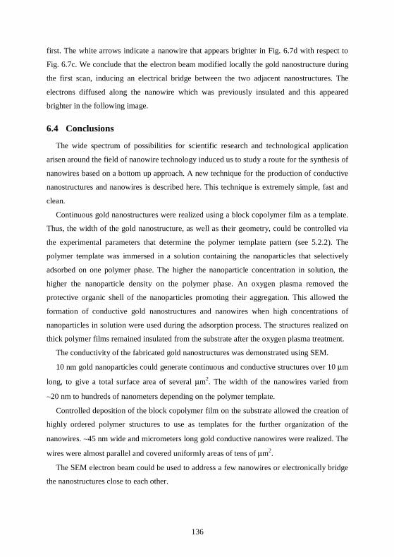
136
first. The white arrows indicate a nanowire that appears brighter in Fig. 6.7d with respect to
Fig. 6.7c. We conclude that the electron beam modified locally the gold nanostructure during
the first scan, inducing an electrical bridge between the two adjacent nanostructures. The
electrons diffused along the nanowire which was previously insulated and this appeared
brighter in the following image.
6.4 Conclusions
The wide spectrum of possibilities for scientific research and technological application
arisen around the field of nanowire technology induced us to study a route for the synthesis of
nanowires based on a bottom up approach. A new technique for the production of conductive
nanostructures and nanowires is described here. This technique is extremely simple, fast and
clean.
Continuous gold nanostructures were realized using a block copolymer film as a template.
Thus, the width of the gold nanostructure, as well as their geometry, could be controlled via
the experimental parameters that determine the polymer template pattern (see 5.2.2). The
polymer template was immersed in a solution containing the nanoparticles that selectively
adsorbed on one polymer phase. The higher the nanoparticle concentration in solution, the
higher the nanoparticle density on the polymer phase. An oxygen plasma removed the
protective organic shell of the nanoparticles promoting their aggregation. This allowed the
formation of conductive gold nanostructures and nanowires when high concentrations of
nanoparticles in solution were used during the adsorption process. The structures realized on
thick polymer films remained insulated from the substrate after the oxygen plasma treatment.
The conductivity of the fabricated gold nanostructures was demonstrated using SEM.
10 nm gold nanoparticles could generate continuous and conductive structures over 10 µm
long, to give a total surface area of several µm2. The width of the nanowires varied from
∼20 nm to hundreds of nanometers depending on the polymer template.
Controlled deposition of the block copolymer film on the substrate allowed the creation of
highly ordered polymer structures to use as templates for the further organization of the
nanowires. ∼45 nm wide and micrometers long gold conductive nanowires were realized. The
wires were almost parallel and covered uniformly areas of tens of µm2.
The SEM electron beam could be used to address a few nanowires or electronically bridge
the nanostructures close to each other.
137
Template assisted nanowire fabrication is a common technique to obtain order arrays of
nanowires. Block copolymer films have been often used as such templates. However, the
nanowires have been usually formed perpendicular to the film plane and hexagonal arrays
[94]. On the contrary, in our work we describe the fabrication of nanowires lying in the plane
of the film. This approach has the advantage to combine the formation of µm-long nanowires,
with the possibility to laterally order them. In addition, the nanowires can be transferred to
hard surfaces.
The study of nanowire electrical transport properties is important for its characterization,
electronic device applications and the investigation of unusual transport phenomena arising
from one-dimensional quantum effects. Important factors that determine the electrical
transport properties of nanowires include the wire diameter (important for both classical and
quantum size effects), material composition, surface conditions, crystal quality, and the
crystallographic orientation along the wire axis. Conductive AFM [151] could be used to
study the nanostructure conductivity: a metal pad may be evaporated on the nanowire
structures and could be electrically connected to a measuring instrument. Single nanowires
may be addressed using the metallic tip, to induce a current in the wire. Current
measurements would suggest to which extent the nanowire conducting behaviour is affected
by quantum effects [152]. The same sample could be investigated with a modified SEM able
to produce a conductivity map of the surface; in this case the wires would be addressed by the
electron beam in stead of the metallic tip. This kind of measurement will be set up in the
future for further investigation of the nanostructure conductivity.

139
Chapter 7
7 Conclusions and Outlook
The aim of this work was the lateral organization of nanoparticles made of various
materials on the micrometer and nanometer scale, using the self-assembling and self-
organizing properties of homopolymers and block copolymers. These bottom-up approaches
for the creation of nanoparticle patterns on surfaces may offer in some cases an alternative to
common lithographic techniques that often require expensive capital equipment and
infrastructures.
Part of this work concerned the study of the fluorescence properties of Mn2+ doped ZnS
nanoparticles. Core and core/shell ZnS:Mn nanoparticles were found to possess exceptionally
long fluorescence lifetimes in the millisecond range and high performances in terms of
photostability. These characteristics are very advantageous for time-gated fluorescence
detection methods. This is a powerful technique but usually requires a fast and expensive
equipment due to the necessity to work in the ns and µs regime. As ZnS:Mn nanoparticles
exhibited ms fluorescence lifetime, the electronic required was not particularly sophisticated
and the cost of the detection instrument could be kept low. A simple set up for time-gated
fluorescence detection was assembled and fluorescence lifetime measurements were
performed.
Waveguide-based sensors receive at the moment great attention by industries due to their
high sensitivity and reduced sample and reagent consumption. The possibility to use ZnS:Mn
nanoparticles in combination with this kind of sensors was explored. Using the WIOS
instrument it was demonstrated that ZnS:Mn nanoparticles may be used as mass labels for
refractometric measurements.
140
A route for the improvement of waveguide-based sensor sensitivity and accuracy is the
combination of fluorescence and refractometric detection. In the specific case of ZnS:Mn
nanoparticles, which absorb UV light, a compact waveguide-based sensor may be developed
using an excitation source external to the waveguide. Their orange emission could be
collected by the waveguide itself or, alternatively, by an external detection system.
In conclusion, our study on ZnS:Mn nanoparticles identified them as promising labels for
time-gated fluorescence and refractometric detection which may contribute to the
development of high sensitive and low costs sensors.
Nanoparticles are the ideal building blocks for the creation of surface structures with new
functionalities. However, the first step towards the realization of concrete devices consists of
the ability to laterally organize these nanoparticles and thus to form patterns of nanoparticles.
Most successful techniques for the fabrication of nanoparticle arrays involve crystal
growth on or within well-defined two dimensional or confined three-dimensional structures.
Polymer structures are mainly used as templates to guide the crystal nucleation and growth,
and give various sizes and shapes. A number of templates have been employed including, for
example, inverse block copolymer micellar systems in which metal ions are located in the
polar phase and further reduction of the metal ions results in the formation of metallic
nanoparticles within the micelles [153]. Alternatively, different kinds of metal have been
evaporated on thin block copolymer films having a fingerprint-like pattern with the two
blocks alternating along the surface and the selective decoration of one polymer phase
[152;154]. In contrast, this work describes two approaches for the formation of patterns of
nanoparticles synthesized before formation of the polymer structure. This means that a very
wide range of objects – metallic, semiconductor nanoparticles or even organic molecules –
can be used.
The first method developed for the creation of nanoparticle patterns is based on the
demixing behaviour of polymer blends. In agreement with numerical simulations performed
by other groups, the nanoparticles organized within a polymer phase or at its boundary and
patterns of nanoparticles were successfully created. The polymer could also be removed by
oxygen plasma so that the nanoparticles were patterned directly on the substrate surface.
This technique is based on the same phenomena observed in the partitioning of chemical
species in immiscible two-phase solvent systems, often used by chemists as a purification
method [16]. However, to our knowledge the technique has not been used to structure thin
141
polymer/nanoparticle composite films with the intention of forming patterns of nanoparticles
on a surface. Further studies have shown that this technique can be used to organize biological
molecules on surfaces. For examples, fluorescently labelled Bovine Serum Albumin
molecules have been organized in the Dextran phase of a Dextran/polyethylene glycol
demixed film [155]. The successful use of the polymer demixing technique to organize
biomolecules on surfaces opens up prospects for a wide field of applications in biochip
technology.
The technique described is extremely simple, fast and low cost. The pattern size and shape
can be controlled by experimental parameters such as the rotation speed, the substrate surface
energy and the blend composition. Micro-contact printing of thiols was used to create a
surface energy variation on the substrate and induce an alignment of the polymer domains.
Thus, stochastic and ordered patterns of nanoparticles on surfaces with typical sizes in the
micrometer and sub-micrometer regime were realized. The distribution of single nanoparticle
within the polymer phases was studied using confocal microscopy, atomic force microscopy
and transmission electron microscopy (TEM results not shown).
The influence of the nanoparticles on the demixing behaviour of immiscible polymer
blends was also studied. We observed that the resulting film structure is strongly influenced
by the concentration of the nanoparticles in the polymer blend, making difficult to predict and
tailor the nanoparticle patterns a priori.
The creation of patterns of nanoparticles in the micrometer and sub-micrometer range can
find different kinds of application in fields that range from optics to biosensors technology.
For example, polymer films presenting structure sizes comparable to a visible wavelength can
be used to create special coatings for optical components. The organization of the gold
nanoparticles in the desired pattern within the polymer film using polymer demixing could
represent a valid alternative to the laser processing for mask fabrication in micro-powder
blasting technique [156], with the advantage that the time of processing would not rely on the
patterned surface. The same reduction of time of processing could be achieved in those
technologies that make use of polymer/nanoparticle composite film such as solar cells [41],
lithium batteries [64] and magnetic storage [67] technologies.
The second technique developed is based on the decoration of polymer films presenting
different polymer phases at the surface with nanoparticles. Phase-separated polymer films are
thus templates for the further organization of the nanoparticles. The templates were realized
using both immiscible homopolymer blends and block copolymers.
142
With this technique CdSe, Au and CoPt3:Cu nanoparticles were organized in the
micrometer and sub-micrometer range using demixed polymer films as templates and in the
nanometer range using the block copolymer templates. Moreover, the control of the coating
speed or, alternatively, of the substrate surface energy allowed the creation of a double level
of pattern structure, at micrometer and nanometer length scale, on the same film. Oxygen
plasma treatments could be used to remove the polymer film and transfer the nanoparticle
pattern to the substrate surface.
Mixing the nanoparticles inside the polymer blend allows the formation of a large particle-
polymer interface. This is important for those applications where the nanoparticles catalyze
reactions at their surfaces with the polymer film. Nanoparticles organized via decoration of
the polymer films present a reduced polymer/nanoparticle interface. However, a second
polymer layer might be coated or deposited on the first, once the nanoparticles are already
organized on the polymer film. The possibility to form the polymer template before patterning
the nanoparticles allows better control over the template itself and thus prediction of the
nanoparticle pattern.
The creation of nanoparticle patterns on hard surfaces has also many potential applications.
Nanoparticle patterns on hard surfaces having typical length scale varying from the
micrometer to the nanometer may be used, for example, as reactive sites, e.g. cobalt
nanoparticles may catalyze the carbon nanotubes growth on a chip. Gold nanoparticles may
be patterned on a biochip and functionalized in order to bind specific biomolecules.
Moreover, a surface presenting the nanoparticles organized as the fingerprint-like pattern
typical of block copolymers presents an increased surface with respect to a flat substrate and
thus a higher density of detection sites.
It was shown that the coverage of polymer surfaces with gold nanoparticles depends on the
concentration of nanoparticles in solution. Acting on this parameter, we were able to induce a
certain degree of aggregation of the nanoparticles on the polymer template. Successive
oxygen plasma treatment caused the removal of the nanoparticle protective organic shell
promoting their further aggregation. In this way we were able to produce µm-long gold
nanowires and nanostructures. The width of these structures varied from ~25 nm to some µm.
The conductivity of these gold nanostructures was demonstrated using the scanning
electron microscopy. Nanowires realized on thick polymer films (≥ 20 nm) masked the
polymer template from the action of the oxygen plasma so that they remained isolated from
the substrate at the end of the process. Thus, charging of the sample occurred when the
143
structures were illuminated by the electron beam. We observed the propagation of the
electrons along the gold nanostructures for µm long distances from the illumination area.
The electron beam could be used as an active element to charge selected nanowires or to
modify the gold nanostructure.
The technique described for the formation of conductive nanowires may be extended in the
future to different kinds of metal nanoparticles and block copolymers.
The self-assembly of nanowires may present a way to construct unconventional devices
that do not rely on improvements in photo-lithography and, therefore, do not necessarily
imply increasing fabrication costs. Devices made from nanowires have several advantages
over those made by photolithography. In addition, unlike traditional silicon processing,
different materials can be simultaneously used in nanowire devices to produce diverse
functionalities. Not only wires of different materials can be combined, but a single wire can
be made of different materials.
Sensors for chemical and biochemical substances with nanowires as the sensing probe are
a very attractive application area. Nanowire sensors will potentially be smaller, more
sensitive, demand less power, and react faster than their macroscopic counterparts. Arrays of
nanowire sensors could, in principle, achieve nanometer scale spatial resolution and therefore
provide accurate real-time information regarding not only the concentration of a specific
analyte but also its spatial distribution. For example, a pH sensor was made by covalently
linking an amine containing silane to the surface of the nanowire [157].The variation in
surface charge densities regulates the conductance of the nanowire. The same type of
approach was used for the detection of the binding of biomolecules, such as streptavidin using
biotin-modified nanowires. Favier et al. used a similar approach, making a nanosensor for the
detection of hydrogen out of an array of palladium nanowires between two metal contacts
[158].

145
Appendix A
A Table of References
[1] ‘What I want to talk about is the problem of manipulating and controlling things on a
small scale. As soon as I mention this, people tell me about miniaturization, and how far it has
progressed today. […] But that's nothing; that's the most primitive, halting step in the
direction I intend to discuss. It is a staggeringly small world that is below’. R. Feymann,
during the talk There's Plenty of Room at the Bottom at the annual meeting of the American
Physical Society at the California Institute of Technology (Caltech), December 29th 1959.
[2] K. Eric Drexler, Proc. Natl. Acad. Sci. USA 78 (9) (1981) 5275.
[3] K. J. Klabunde, Free Atoms, Cluster, and Nanoscale particles, Academic Press, San
Diego 1994, pp 2, 36. K. J. Klabunde, C. Mohs, in Chemistry of Advanced Materials: An
Overview, L. V. Interrante, M. J. Hampden-Smith, Wiley-VHC, New York 1998, p. 271. K. J.
Klabunde, Nanoscale Materials in Chemistry, Wiley, New York 2001, ch. 1.
[4] Although already in 1857 Michael Faraday remarked that ‘a mere variation in size of
gold particles gives rise to a variety of resultant colours’. M. Faradays, Philos. Trans. R. Soc.
147 (1857) 145.
[5] A. P. Alivisatos, J. Phys. Chem. 100 (1996) 13226. A. P. Alivisatos, Science 271
(1996) 933. J. de Jongh, Physics and Chemistry of Metal Cluster Compounds, Kluwer
Academic Publishers, Dordrecht, 1994.
[6] K. J. Klabunde, Nanoscale materials in Chemistry, Wiley-Interscience, New York,
2001, ch.2 and 3.
146
[7] J. S. Bradley, Clusters and Colloids from theory to applications, ed. G. Shmid, VCH
1994, ch. 6.
[8] J. Dutta, H. Hofmann, Encyclopedia of Nanoscience and Nanotechnology, ed. H. S.
Nalwa, vol. 10, p. 1, American Scientific Publisher, 2003.
[9] V. Ya. Shevchenko, A. E. Madison, V. E. Shudegov, Glass Phys. Chem. 29 (2003) 577.
[10] G.M. Whitesides and B. Grzybowski, Science 295 (2002) 2418.
[11] Kamien, R. D. Science 299 (2003) 1671.
[12] D. Myers, Surfaces, Interfaces and Colloids - Principles and Applications, Wiley-
WCH, New York, 1999, ch. 4.
[13] J. N. Israelachvili, Intermolecular & Surface Forces, Academic Press, Boston 1992.
[14] G. Strobl, The physics of Polymers, Springer, Berlin 1997.
[15] J. W. Cahn, Transactions of metallurgical society of AIME 242 (1968) 166.
[16] P. A. Albertsson, Partition of cells particles and macromolecules, Wiley Interscience,
USA, 1986.
[17] See e.g. J. Mazur, C. M. Guttman, F. L. McCrackin, Macromolecules 6 (1973) 872.
[18] J. Bashnagel, K. Binder, Macromolecules 28 (1995) 6808. T. Pakula, J. Chem. Phys.
95 (1991) 4685.
[19] J. Kraus, P. Müller-Buschbaum, T. Kuhlmann, D. W. Shubert, M. Stamm, Europhys.
Lett. 49 (2000) 210.
[20] R. L. Jones, C. L. Soles, F. W. Starr, E. K. Lin, J. L. Lenhart, W. Wu, D. L. Goldfarb,
M. Angelopoulos, SPIE Proc. 4690 (2002) 342.
[21] J. A. Forrest, K. Dalnoki-Veress, J. R. Dutcher, Phys Rev. E 56 (1997) 5705.
[22] S. Reich, Y. Cohen, J. Polym. Sci.: Polym. Phys. Ed. 19 (1981) 1255.
[23] J. H. van Zanten, W. E. Wallace, W. Wu, Phys. Rev. E 53 (1996) R2054. J. L. Keddie,
R. A. L. Jones, R. A. Cory, Faraday Discuss. 98 (1994) 219.
[24] R. C. Ball, R. L. Essery, J. Phys: Condens. Matter 2 (1990) 10303. R. A. L. Jones, L.
J. Norton, E. J. Kramer, F. S. Bates, P. Wiltzius, Phys Rev. Lett. 66 (1991) 1326.
[25] K. Tanaka, A. Takahara, T. Kajiyama, Macromolecules 29 (1996) 3232. S. Walheim,
M. Böltau, J. Mlynek, G. Krausch, U Steiner, Macromolcules 30 (1997) 4995.
[26] G. Krausch, E. J. Kramer, Appl. Phys. Lett. 64 (1994) 2655. M. Böltau, S. Walheim, J.
Mlynek, G. Krausch, U. Steiner, Nature 391 (1998) 877.
147
[27] See for example: S. H. Anastasidas; T. P. Russel; S. K. Satija; C. F. Majkrzak, J.
Chem. Phys.92 (1990) 5677. G. J. Kellogg; D. G. Walton; A. M. Mayes, P. Lambooy, T. P.
Russell, P. D. Gallagher, S. K. Satija, Phys. Rev. Lett.76 (1996) 2503. P. Mansky, Y. Liu, E.
Huang, T. P. Russell, C. J. Hawker Science 275 (1997) 1458.
[28] I. I. Potemkin, E. Yu. Kramarenko, A. R. Khokhlov, R. G. Winkler, P. Reineker, P.
Eibeck, J. P. Spatz, M. Möller, Langmuir 15 (1999) 7290. E. Yu. Kramarenko; I. I. Potemkin;
A. R. Khokhlov, R. G. Winkler, P. Reineker, Macromolecules 32 (1999) 3495.
[29] G. Coulon, T. P. Russell, V. R. Deline, P. F. Green, Macromolecules 22 (1989) 2581.
M. Maaloum, D. Ausserre, D. Chatenay, G. Coulon, Y. Gallot, Phys Rev. Lett. 68 (1992)
1575.
[30] M. Vacatello, Macromolecules 34 (2001) 1946.
[31] D. H. Cole, K. R. Shull, P. Baldo, L. Rehn, Macromolecules 32 (1999) 771.
[32] Z. Y. Zhong, B. Gates, Y. N. Xia, D. Qin, Langmuir 16 (2000) 10369. M. Zahn, J.
Nanoparticle Res. 3 (2001) 73. J. Shi, S. Gider, K. Babcock, D. D. Awschalom, Science 271
(12996) 937.
[33] C. Lebreton, C. Vieu, A. Pépin, M. Mejias, F. Carcenac, Y. Jin, H. Launois,
Microelectr. Eng. 41/42 (1998) 507. A. D. Yoffe, Adv. Phys. 50 (2001) 1. L. P.
Kouwenhoven, D. G. Austing, S. Tarucha, Rep. Prog. Phys. 64 (2001) 701.
[34] T. Ito, S. Okazaki, Nature 406 (2000) 1027.
[35] A. Kumar, H. A. Biebuyck, G. M. Whitesides, Langmuir 10 (1994) 1498.
[36] K. Y. Suh, Y. S. Kim, and H. H. Lee, Adv. Mater. 13 (2001) 1386.
[37] An admirable example is the famous Lycurgus Cup from the forth century A.D. where
gold nanoparticles with a diameter below 20 nm are used as glass dopant conferring it a bright
red colour. During the Middle age colloidal gold nanoparticles have been use in many
churches to produce the red colour of stained glass windows.
[38] P. Mulvaney, MRS Bulletin 26 (2001) 1009.
[39] V. I. Klimov, A. A. Mikhailovsky, S. Xu, A. Malko, J. A. Hollingsworth, C. A.
Leatherdale, H. Eisler, M. G. Bawendi, Science 290 (2000) 314. V. C. Sundar, H. J. Eisler, M.
G. Bawendi, Adv. Mat. 14 (2002) 739.
[40] V. L. Colvin, M. C. Shlamp, A. P. Alivisatos, Nature 370 (1994) 354. S. Coe, W. K.
Woo, M. Bawendi, V. Bulovic, Nature 420 (2002) 800. N. Tessler, V. Medvedev, M. Kazes,
S. H. Kan, U. Banin, Science 295 (2002) 1506.

148
[41] W. U. Huynh, J. J. Dittmer, A. P. Alivisatos, Science 295 (2002) 2425.
[42] H. Weller, Angew. Chem. Int. Ed. 37 (1998) 1658. D. L. Klein, R. Roth, A. K. L. Lim,
A. P. Alivisatos, P. L. McEuen, Nature 389 (1999) 699.
[43] A. Henglein, A. Fojtik, H. Weller, Ber. Bunsen-Ges. 91 (1987) 441.
[44] T. Trindade, P. O’Brien, N. L. Pickett. Chem. Mater. 13 (2001) 3843.
[45] W. J. Parak, D. Gerion, T. Pellegrino, D. Zanchet, C. Micheel, S. C. Williams, R.
Boundreau, M. A. Le Gros, C. A. Larabell, A. P. Alivisatos, Nanotechnology 13 (2003) R15.
X. Gao, S. Nie, Trends in Biotech. 21 (2003) 371. A. J. Sutherland, Curr. Opin. Solid St. M. 6
(2002) 365. E. Dujardin, S. Mann, Adv. Eng. Mat. 4 (2002) 461.
[46] R. P. Haugland, Handbook of Fluorescent Probes and Research Products, 9th edition,
Molecular Probes, p. 46.
[47] For example a complex four-laser confocal system providing six different excitation
wavelengths was recently developed. See D. J. Graves, H. J. Su, S. Surrey, P. Fortina,
BioTechniques 32 (2002) 346.
[48] A set of probes has been produced that afforded a spectral range from 400 nm to 2 µm
in the peak emission by varying the material and the size of the quantum dots. Bruchez et al.
imaged fluorescently labelled 3T3 mouse fibroblast cells using two different sizes of
CdSe/CdS core/shell nanocrystals enclosed in a silica shell. See M. Bruchez Jr., M. Moronne,
P. Gin, S. Weiss, A. P. Alivisatos, Science 281 (1998) 2013.
[49] W. C. W. Chan, S. Nie, Science 281 (1998) 2016.
[50] B. Dubertret, P. Skourides, D. J. Norris, V. Noireaux, A. H. Brivanlou, A. Libchaber,
Science 298 (2002) 1759.
[51] M. Dahan, S. Lévi, C. Luccardini, P. Rostaing, B. Riveau, A. Triller, Science 302
(2003) 442.
[52] A. M. Derfus, C. W. Chan, S. N. Bathia, Nano Lett. 4 (2004) 11.
[53] J. R. Lakowicz, I. Gryczynski, Z. Gryczynski, C. J. Murphy, J. Phys. Chem. B 103
(1999) 7613. J. R. Lakowicz, I. Gryczynski, Z. Gryczynski, K. Nowaczyk, C. J. Murphy,
Anal. Biochem. 280 (2000) 128.
[54] See for example: N. N. Mamedova, N. A. Kotov, A. L. Rogach, J. Studer, Nano Lett.
1 (2001) 281. I. Willner, F. Patolsky, J. Wasserman, Angew. Chem. Int. Ed. Engl. 40 (2001)
1861. S. R. Bigham, J. L. Coffer, J. Cluster Sci. 11 (2000) 359. I. Sondi, O. Siiman, S.
Koester, E. Matijevic, Langmuir 16 (2000) 3107. H. M. Chen, X. F. Huang, L. Xu, J. Xu, K.
149
J. Chen, D. Feng, Superlatt. Microstruct. 27 (2000) 1. T. Torimoto, M. Yamashita, S.
Kuwabata, T. Sakata, H. Mori H, H. Yoneyama, J. Phys. Chem. B 103 (1999) 8799.
[55] J. Aldana, Y. A: Wang, X. Peng, J. Am. Chem. Soc. 123 (2001) 8844.
[56] D. Gerion, F. Pinaud, S. C. Williams, W. J. Parak, D. Zanchet, S. Weiss, A. P.
Alivisatos, J. Phys. Chem. B 105 (2001) 8861.
[57] H. Mattoussi, J. M. Mauro, E. R. Goldman, G. P. Anderson, V. C. Sundar, F. V.
Mikulec, M. G. Bawendi, J. Am. Chem. Soc. 122 (2000) 12142. E. R. Goldman, G. P.
Anderson, P. T. Tran, H. Mattoussi, P. T. Charles, J. M. Mauro, Anal. Chem. 74 (2002) 841.
D. Gerion, W. J. Parak, S. C. Williams, D. Zanchet, C. M. Micheel, A. P. Alivisatos, J. Am.
Chem. Soc. 124 (2002) 7070. F. Pinaud, D. King, H. P. Moore, S. Weiss, J. Am. Chem. Soc.
126 (2004) 6115.
[58] M. Bäumle, S. Stamou, J. M. Segura, R. Hovius, H. Vogel, Langmuir 20 (2004) 3828.
[59] V. V. Ginzburg, F. Qiu, M. Paniconi, G. Peng, D. Jasnow, A. C. Balazs, Phys. Rev.
Lett. 82 (1999) 4026. Y. Tang, Y. Ma, J. Chem. Phys. 116 (2002) 7719.
[60] M. Laradji, G. MacNevin, J. Chem. Phys. 119 (2003) 2275.
[61] J. Y. Lee, Z. Shou, A. C. Balazs, Phys. Rev. Lett. 91 (2003) 136103. J. Y. Lee, Z.
Shou, A. C. Balazs, Macromolecules 36 (2003) 7730.
[62] V. L. Pasyuk, H. J. Lauter, G. P. Gordeev, P. Müller-Buschbaum, B. P. Toperverg, M.
Jernenkov, W. Petry, Langmuir 19 (2003) 7783. V. Lauter-Pasyuk, H. J. Lauter, D. Ausserre,
Y. Gallot, V. Cabuil, B. Hamdoun, E. I. Kornilov, Phys. B 248 (1998) 243. J. Y. Lee, R. B.
Thompson, D. Jasnow, A. C. Balazs, Macromolecules 35 (2002) 4855.
[63] G. K. Chandler, D. Pletcher, J. Appl. Electrochem. 16 (1986) 62. G. Tourillon, F.
Garnier, G. A. Grunawardena, D. Pletcher, J. Phys. Chem. 88 (1984) 5281.
[64] J. E. Park, S. G. Park, A. Koukitu, O. Hatozaki, N. Oyama, Synth. Mat. 140 (2004)
121.
[65] S. Sun, C.B. Murray, D. Weller, L. Folks, A. Moser, Science 287 (2000) 1989.
[66] T. Coradin, J. Larionova, A. A. Smith, G. Rogez, R. Clerac, C. Guerin, G. Blondin, R.
E. P. Winpenny, C. Sanchez, T. Mallal, Adv. Mater. 14 (2002) 896. M. Clemente-León, E.
Coronado, A. Forment-Aliaga, J. M. Martínez-Agudo, P. Amorós, Polyhedron 22 (2003)
2395. S. Willemin, G. Arrachart, L. Lecren, J. Larinova, T. Coradin, R. Clérac, T. Mallah, G.
Guérin, C. Sanchez, New J. Chem. 27 (2003) 1533.
150
[67] D. Ruiz-Molina, M. Mas-Torrent, J. Gómez, A. I. Balana, N. Domingo, J. Tejada, M.
T. Martínez, C. Rovira, J. Veciana, Adv. Mater 15 (2003) 42.
[68] F. Ribot, C. Sanchez, Comments Inorg. Chem. 20 (1999) 327. G. Kickelbick, U.
Schubert, Monatsh. Chem. 132 (2001) 13. U. Schubert, Chem. Mater. 13 (2001) 3487. U.
Schubert, Organic/Inorganic Hybrid Materials, ed. F.D. Blum and R.M. Laine, Electronic
Publ. Services, Hattiesburg 2003. F. Palacio, P. Olietea, U. Schubert, I. Mijatovic, N. Hüsing,
H. Peterlikc, J. Mater. Chem. 14 (2004) advance article.
[69] J. P. Hoogenboom, D. L. J. Vossen, C. Faivre-Moskalenko, M. Dogterom, Appl. Phys.
Lett. 80 (2002) 4828.
[70] A. A. Mamedov, A. Belov, M. Giersig, N. N. Mamedova, N. N. Kotov, J. Am. Chem.
Soc. 123 (2001) 7738.
[71] Y. Yin, Y. Lu, B. Gates, and Y. Xia, J. Am. Chem. Soc. 123 (2001) 8718.
[72] A. Ulman, Adv. Mater. 3 (1991) 298. J. H. Fendler, Chem. Mater. 8 (1996) 1616. K.
S. Mayya, V. Patil, M. Kumar, M. Shastry, Thin Solid Films 312 (1998) 308.
[73] A. J. Hurd, D. W. Schaefer, Phys. Rev. Lett. 54 (1985) 1043.
[74] M. Kondo, K. Shinozaki, L. Bergstrom, N. Mizutani, Langmuir 11 (1995) 394. H. W.
Deckman, J. H. Dunsmuir, S. M. Gruner, J. Vac. Sci. Technol. B 7 (1989) 1832. F. Lenzmann,
K. Li, A. H. Kitai, H. D. H. Stover, Chem. Mater. 6 (1994) 156. K. U. Fulda and B. Tieke,
Adv. Mater. 6 (1994) 288. F. Burmeister, C. Schafle, T. Matthes, M. Bohmisch, J. Boneberg,
P. Leiderer, Langmuir 13 (1997) 2983.
[75] J. Aizenberg, P. V. Braun, P. Wiltzius, Phys. Rev. Lett. 84 (2000) 2997.
[76] M. Himmelhaus, H. Takei, Phys. Chem. Chem. Phys. 4 (2002) 496.
[77] U. Jonas, A. del Campo, C. Krüger, G. Glasser, D. Boos, PNAS 99 (2002) 5034.
[78] K. M. Chen, X. Jiang, L. C. Kimerling, P. T. Hammond, Langmuir 16 (2000) 7825.
[79] I. Lee, H. Zheng, M. F. Rubner, P. T. Hammond, Adv. Mater. 14 (2002) 572.
[80] B. Prével, L. Bardotti, S. Fanget, A. Hannour, P. Mélinon, A. Perez, J. Gierak, G.
Faini, E. Bourhis, D. Mailly, Appl. Surf. Sci. 226 (2004) 173.
[81] N. Lu, X. Chen, D. Molenda, A. Naber, H. Fuchs, D. V. Talapin, H. Weller, J. Muller,
J. M. Lupton, J. Feldmann, A. L. Rogach, L. Chi, Nano Lett. 4 (2004) 885.
[82] A. Gourishankar, S. Shukla, R. Pasricha, M. Sastry, K.N. Ganesh, Curr. Appl. Phys.,
In Press, (2004).
[83] C. A. Mirkin, R. L. Letsinger, R. C. Mucic, J. J. Storhoff, Nature 382 (1996) 607.
151
[84] P. Alivisatos, K. P. Johnsson, X. Peng, T. E. Wilson, C. J. Loweth, M. Bruchez, P. G.
Schultz, Nature 382 (1996) 609.
[85] R. Elghanian, J. J. Storhoff, R. C. Mucic, R. L. Letsinger, C. A. Mirkin, Science 277
(1997) 1078.
[86] T. Takahagi, S. Huang, G. Tsutsui, H. Sakaueand, S. Shingubara, Mater. Res. Soc.
Symp. Proc. 707 (2002) 87.
[87] J. Priestley, The History and Present State of Electricity with Original Experiments,
2nd ed, J. Dodsley, London 1769. H. A. Pohl, Dielectrophoresis, Cambridge University Press,
Cambridge, UK, 1978.
[88] M. Parthasarathy, D. Klingenberg, Mater. Sci. Eng. R. 17 (1996) 57. U. Dassanayake,
S. Fraden, A. van Blaaderen, J. Chem. Phys. 112 (2000) 3851.
[89] R. W. Zehner, W. A. Lopes, T. L. Morkved, H. Jaeger, L. R. Sita, Langmuir 14 (1998)
241.
[90] Y. Fink, A. M. Urbas, B. G. Bawendi, J. D. Joannopoulos, E. L. Thomas, J. Lightwave
Tech. 17 (1999) 1963.
[91] M. R. Bockstaller, Y. Lapetnikov, S. Margel, E. L. Thomas, J. Am. Chem. Soc. 125
(2003) 5276.
[92] R. S. Wagner, W. C. Ellis, Appl. Phys. Lett. 4 (1964) 89.
[93] C. R. Martin, Science 266 (1994) 1961. G. A. Ozin, Adv. Mater. 4 (1992) 612. R. J.
Tonucci, B. L. Justus, A. J. Campillo, C. E. Ford, Science 258 (1992) 783.
[94] T. Thurn-Albrecht, J. Schotter, G. A. Kästle, N. Emley, T. Shibauchi, L. Krusin-
Elbaum, K. Guarini, C. T. Black, M. T. Tuominen, T. P. Russell, Science 290 (2000) 2126.
[95] X. Y. Zhang, L. D. Zhang, Y. Lei, L. X. Zhao, Y. Q. Mao, J. Mater. Chem. 11 (2001)
1732. H. Zeng, M. Zheng, R. Skomski, D. J. Sellmyer, Y. Liu, L. Menon, S. Bandyopadhyay,
J. Appl. Phys. 87 (2000) 4718. Y. Peng, H.-L. Zhang, S.-L. Pan, H.-L. Li, J. Appl. Phys.87
(2000) 7405. L. Piraux, J.M. George, J. F. Despres, C. Leroy, E. Ferain, R. Legras, K.
Ounadjela, A. Fert, Appl. Phys. Lett. 65 (1994) 2484. S. Bhattacharrya, S. K. Saha, D.
Chakravorty, Appl. Phys. Lett. 76 (2000) 3896. G. Yi, W. Schwarzacher, Appl. Phys. Lett.74
(1999) 1746.
[96] L. Piraux, S. Dubois, J. L. Duvail, A. Radulescu, S. Demoustier-Champagne, E.
Ferain, R. Legras, J. Mater. Res. 14 (1999) 3042.
[97] G. Yi, W. Schwarzacher, Appl. Phys. Lett. 74 (1999) 1746.
152
[98] D. Routkevitch, T. Bigioni, M. Moskovits, J.M. Xu, J. Phys. Chem. 100 (1996)
14037.
[99] M. P. Zach, K. H. Ng, R. M. Penner, Science 290 (2000) 2120. M. P. Zach, K. Inazu,
K. H. Ng, J. C. Hemminger, R. M. Penner, Chem. Mater. 14 (2002) 3206.
[100] CdSe nanoparticles and nanorods were synthesized by Isabelle Geissbuehler in the
Institut des sciences et ingénierie chimiques of EPFL (Lausanne, CH). Reference articles: C.
B. Murray, D. J. Norris, M. G. Bawendi, J. Am. Chem. Soc. 115 (1993) 8706. L. Qu, Z. A.
Peng, X. Peng Nano Lett. 1 (2001) 333. For nanorods synthesis: X. Peng, L. Manna, W.
Yang, J. Wickham, E. Scher, A. Kadavanich, A. P. Alivisatos, Nature 404 (2000) 59. Z. Peng,
X. Peng, J. Am. Chem. Soc. 123 (2001) 1389.
[101] S. V. Gaponenko, Optical properties of Semiconductor Nanocrystals, Cambridge
University Press, Cambridge, 1998. Al. L. Efros, M. Rosen, Annu. Rev. Mat. Sci. 30 (2000)
475.
[102] O. Schmelz, A. Mews, Th. Basche, A. Herrmann, K. Müllen, Langmuir 17 (2001)
2861.
[103] M. Kuno, D. P. Fromm, H. F. Hamann, A. Gallagher, D. J. Nesbitt, J. Chem. Phys.
115 (2001) 1028.
[104] S. A. Empedocles, D. J. Norris, M. G. Bawendi, Phys. Rev. Lett. 77 (1996) 3873. J.
Tittel, W. Göhde, F. Koberling, A. Mews, A. Kornowski, H. Weller, A. Eychmüller, T.
Basche, Ber. Bunsenges. Phys. Chem. 101 (1997) 1626. S. Empedocles, M. Bawendi, Acc.
Chem. Res. 32 (1999) 389. K. T. Shimizu, R. G. Neuhauser, C. A. Leatherdale, S. A.
Empedocles, W. K. Woo, M. G. Bawendi, Phys. Rev. B 63 (2001) 205316. F. Koberling, A.
Mews, Th. Basche, Adv. Mater. 13 (2001) 672.
[105] M. Nirmal, B. O. Dabbousi, M. G. Bawendi, J. J. Macklin, J. K. Trautman, T. D.
Harris, L. E. Brus, Nature 383 (1996) 802.
[106] S. Hohng, T. Ha, J. Am. Chem. Soc. 126 (2004) 1324.Al. L. Efros, M. Rosen, M.
Kuno, M. Nirmal, D. J. Norris, M. Bowendi, Phys. Rev. B 54 (1996) 4843.
[107] W. G. J. H. M. van Sark, P. L. T. M. Frederix, D. J. Van den Heuvel, H. C.
Gerritsen, A. A. Bol, J. N. J. van Lingen, C. de Mello Donega, A. Meijerink, J. Phys. Chem. B
105 (2001) 8281.
153
[108] T. D. Krauss, L. E. Brus, Phys. Rew. Lett. 83 (1999) 4840. E. Rabani, B. Hetenyi, B.
J. Berne, J. Chem. Phys. 110 (1999) 5355. S. A. Blanton, R. L. Leheny, M. A. Hines, P.
Guyot-Sionnest, Phys. Rev. Lett. 79 (1997) 865.
[109] Core ZnS:Mn and core/shell ZnS:Mn/SiO2 nanoparticles were synthesized and
characterized by Yvonne Axmann in the Institut des matériaux of EPFL (Lausanne, CH).
Description of her work can be found in: Y. Axmann, Manganese Doped ZnS Nanoparticles:
Synthesis, Particles Sizing and Optical Properties, PhD thesis (2004), EPFL (Lausanne, CH).
Y. Axmann, A. Petri, H. Hofmann, Mat. Res. Soc. Symp. Proc. 789 (2004) N11.23.
[110] K. Sooklal, B. S. Cullum, S. M. Angel, C. J. Murphy, J. Phys. Chem. 100 (1996)
4551
[111] U. Kreibig, M. Vollmer, Optical Properties of Metal Clusters, Springer-Verlag,
Berlin 1996.
[112] CoPt3:Cu and Co nanopartilces were synthesised by Christoph Fromman in the
Institut fur Nanotechnologie of the Forschungszentrum Karlsruhe in der Helmholtz-
Gemeinschaft (Karlsruhe, Germany) and the magnetic properties of their assemblies have
been studied. His work concerning CoPt3:Cu nanoparticles is reported in: C. Frommen, S.
Malik, J.U. Würfel, H. Rösner, C. Didschies, Mater. Lett. 58 (2004) 953.
[113] R. Eckert, Probing single molecules by optical near and far field microscopy, PhD
thesis (2001), University of Basel (CH).
[114] G. K. Binnig, C. F. Quate, C. Gerber, Phys. Rev. Lett. 56 (1986) 930.
[115] G. Meyer, N. M. Amer, Appl. Phys. Lett. 53 (1988) 2400.
[116] E. Ruska, M. Knoll, Z. techn. Physik 78 (1932) 318.
[117] L. Libioulle, A. Bietsch, H. Schmid, B. Michel, E. Delamarche, Langmuir 15 (1999)
300.
[118] E. Delamarche, H. Schmid, A. Bietsch, N. B. Larsen, H. Rothuizen, B. Michel, H.
Biebuyck, J. Phys. Chem. B 102 (1998) 3324.
[119] D. A. Winesett, H. Ade, J. Sokolov, M. Rafailovich, S. Zhu, Polym. Int. 49 (2000)
458. E. Kumacheva, L. Li, M. A. Winnik, D. M. Shinozaki, P. C. Cheng, Langmuir 13 (1997)
2483.
[120] P. Eibeck, Surface induced nano patterns formed by amphiphilic block copolymers,
PhD thesis (1999), University of Ulm (D).
154
[121] G. Marriott, R. M. Clegg, D. J. Arndt-Jovin, T. M. Jovin, Biophys. J. 60 (1991)
1374.
[122] E. Terpetschnig, H. Szmacinski, H. Malak, and J. R. Lakowicz, Biophys. J. 68
(1995) 342.
[123] J. R. Lakowicz, Scanning Microsc. Suppl. 213 (1996).
[124] J. R. Lakowicz, Principles of Fluorescence Spectroscopy, 2nd edition, Kluwer
Academic/Plenum Publishers, New York 1999, p. 239.
[125] M. Dahan, T. Laurence, F. Pinaud, D. S. Chemla, A. P. Alivisatos, M. Sauer, S.
Weiss, Optic Lett. 26 (2001) 825.
[126] S. F. Wuister, I. Swart, F. van Driel, S. G. Hickey, C. de Mello Donega, Nano Lett. 3
(2003) 503.
[127] A. A. Bol, A. Meijerink, Phys. Rev. B 58 (1998), R15997.
[128] G. L. Duveneck, A. P. Abel, SPIE Proceedings 3858 (1999) 1. R. E. Kunz,
Integrated Optics in Sensors: Advances towards Miniaturized Systems for Chemical and
Biochemical Sensing in Design and Application of integrated Optical Circuits and
Components, Ed. E. J. Murphy, Dekker, New York, 1998, ch. 5. G. L. Duveneck, M. Pawlak,
D. Neushäfer, W. Budach, M. Ehrat, SPIE Proceedings 2928 (1996) 98.
129 D. G. Hall, Theory of Waveguides and Devices in Integrated Optical Circuits and
Components, Ed. L. D. Hutcheson, M. Dekker, New York 1987. K. Cottier, Advanced Label-
free Biochemical Sensors Based on Integrated Optical Waveguide Gratings, Theory,
Modelling, Design and Characterization, PhD Thesis (2004), Institute of Microtechnology of
the University of Neuchâtel (Neuchâtel, CH).
[130] M. Wiki, H. Gao, M. Juvet, R. E. Kunz, Biosens. & Bioelectr. 16 (2001) 37.
[131] J. Spinke, N. Oranth, Ch. Fattinger, H. Koller, C. Mangold, D. Voegelin, Sensors &
Actuators B, 38-39 (1997) 256. A. H. Severs, R. B. M. Schasfoort, Biosens. & Bioelectr. 8
(1993) 365. P. E. Buckle. R. J. Davies, T. Kinning, D. Yeung, P. R. Edwards, D. Pollard-
Knight, C. R. Lowe, Biosens. & Bioelectr. 8 (1993) 355.
[132] M. Wiki, R. E. Kunz, Optics Lett. 25 (2000) 463. K. Cottier, M. Wiki, G. Vorin, H.
Gao, R. E. Kunz, Sensors and Actuators B 91 (2003) 241.
[133] A. Grinvald, I. Z. Steinberg, Anal. Biochem. 59 (1974) 583. M. L. Jhonson, Anal.
Biochem. 148 (1985) 471.
155
[134] Fluorescence lifetime measurements were performed by Prof. Xavier Allonas in the
Département de Photochimie Générale of the CNRS of Mulhouse and of the Université de
Haute Alsace.
[135] S. F. Wuister, I. Swart, F. van Driel, S. G. Hickey, C. de Mello Donega, Nano Lett. 3
(2003) 503.
[136] F. Jain, W. Huang, J. Appl. Phys. 85 (1999), 2706.
[137] X. Peng, M. C. Schlamp, V. Kadavanich, A. P. Alivisatos, J. Am. Chem. Soc. 119
(1997) 7019.
[138] T. B. Liverpool, M. Stapper, Europhys. Lett. 40 (1997) 485.
[139] G. Decher, Science 277 (1997) 1232.
[140] Z. Adamczyk, P. Warszynski, Adv. Coll. Int. Sci. 63 (1996) 41. B. Senger, J. C.
Vogel, P. Schaaf, Coll. Surf. A 165 (2000) 255. Z. Adamczyk, Adv. Coll. Int. Sci. 100-102
(2003) 267.
[141] S.J. Strickler, R.A. Berg, J.Chem.Phys. 37 (1962) 814.
[142] J. Hu, L. Li, W. Yang, L. Manna, L. Wang, A. P. Alivisatos, Science 292 (2001)
2060.
[143] H. Tanaka, A. J. Lovinger, D. D. Davis, Phys. Rev. Lett. 72 (1994) 2581.
[144] C. Minelli, I. Geissbuehler, R. Eckert, H. Vogel, H. Heinzelmann, M. Liley, Coll.
Polym. Sci. 282 (2004) 1274.
[145] C. G. Blachford, J. R. Campbell, J. A. Creighton, Surface Science 120 (1982) 435.
[146] M. S. Kunz, K. R. Shull, A. J. Kellock, J. Coll Int. Sci. 156 (1993) 240.
[147] J. P. Spatz, P. Eibeck, S. Mössmer, M. Möller, Macromolecules 33 (2000) 150.
[148] K. Spratte, L. F. Chi, and H. Riegler, Europhys. Lett. 25 (1994) 211. G. Reiter,
l’actualité chimique, 1 (2003) 12.
[149] D. Halliday, R. Resnick, Physics – Part Two, Ed. Ambrosiana, Milan 1982, p.47.
[150] A Guide to Scanning Microscope Observation, Joel Serving Advanced Technologies.
[151] A. Bietsch, M. A. Schneider, M. E. Welland, B. Michel. J. Vac. Sci. Technol. B 18
(2000) 1160.
[152] W. A. Lopes, H. M. Jaegger, Nature 414 (2001) 735.
[153] H. G. Boyen, G. Kästle, F. Weigl, B. Koslowsky, C. Dietrich, P. Ziemann, J. P.
Spatz, S. Riethmüller, C. Hartmann, M. Möller, G. Schmid, M. G. Garnier, P. Oelhafen,
Science 297 (2002) 1533.

156
[154] W. A. Lopes, Phys Rev. E 65 (2002) 31606.
[155] N. Blondiaux, CSEM SA, Neuchâtel (CH). Internal communication.
[156] H. Yagyu, S. Hayashi, O. Tabata, J. Microelectromechanical Syst. 13 (2004) 1.
[157] Y. Cui, Q. Wei, H. Park, C. Lieber, Science 293 (2001) 1289.
[158] F. Favier, E. C. Walter, M. P. Zach, T. Benter, R. M. Penner, Science 293 (2001)
2227.
157
Appendix B
Curriculum Vitae
Name: Caterina Minelli
Date of birth: 13th April 1976
Place of birth: Florence (Italy)
Nationality: Italian
e-mail: [email protected]
Professional Address: CSEM SA
Jaquet Droz 1,
CH-2007, Neuchâtel (CH).
Professional Phone: +41.32.720.52.72
Education and work experience
2002 Apr / Present – Centre Suisse d’Electronique et de Microtechnique (CSEM),
(Neuchâtel, Switzerland). PhD student in the Nanoscale Technology & Biochemical Sensing
group of Dr. Raphael Pugin, under the supervision of Dr. Martha Liley (CSEM SA) and
Prof. Horst Vogel, head director of the Laboratoire de Chimie Physique des Polymères et
Membranes (Département de Chimie) of the Ecole Polytechnique Fédérale de Lausanne
(EPFL), (Lausanne, Switzerland).
2000 Dec / 2001 Mar - University of Florence (Italy), study of microstripe silicon devices
and measurement automatization using flying probes.
2000 Oct – Diploma in Physics (Laurea, marks: 110/110 cum laude). Specialization in
Nuclear and Subnuclear Physics, University of Florence (Italy). Dissertation in Elementary
Particle Physics ‘Radiation-hard Microstripe Silicon Detectors for the CMS Tracker’, under
the supervision of Prof. Ettore Focardi. This work is part of the activity performed for the
CMS experiment at LHC in CERN (Geneva, CH).

158
1995 Jul - High School Diploma in Scientific Studies (marks: 60/60) at the Liceo
Scientifico "Piero Gobetti" of Florence (Italy).
Publications
• C. Minelli et al., Organization of nanoparticles via thin polymer film structuring,
CSEM Scientific and Technical report 2003 (2004).
• C. Minelli et al., Organization of Nano-Sale Objects via Polymer Demixing,
published on line in Colloid & Polymer Science (2004).
• C. Minelli et al., Nano-Structuring by Molecular Self-Assembly, Chimia 57 (2003)
646.
• C. Minelli et al., The Organization of Nanoparticles Using Polymer Demixing,
CSEM Scientific and Technical report 2002 (2003).
• Buffini et al., Characterization of neutron irradiated silicon microstrip detectors,
Neucl. Instr. and Meth. In Phys. Res. A 476 (2002) 734.
• C. Minelli et al., Fluorescent Quantum Dots for Biochemical Sensing, CSEM
Scientific and Technical report 2001 (2002).
• R. Eckert, C. Minelli, M. Liley, and H. Heinzelmann, Single Particle Fluorescence
Detection – High Resolution Microscopy, Temporal Behaviour. Towards chirality,
Europ. Cells and Mat. 2. (2001) 88.
Conferences
• C. Minelli et al., Organization of metal and semiconductor Nanoparticles on
Surfaces using Block-copolymer self-assembled structures, Nanofair 2004, St.
Gallen (Switzerland), 14-16 September 2004 (Poster).
• C. Minelli et al., Decoration of Poly(styrene-b-vinylpyridine) film with Metal and
Semiconductor Nanoparticles, Annual meeting of the Swiss Physical Society,
Neuchâtel (Switzerland), 3-4 March 2004 (Oral Contribution).
• C. Minelli et al., Organization of Nano-Sale Objects via Thin Polymer Film
Structuring, New Trends in Surface Science, Fribourg (Switzerland), 23 January
2004 (Oral Contribution).
• C. Minelli et al., Organization of Nano-Sale Objects via Thin Polymer Film
Structuring, Nanopatterns and Nanostructures at Interfaces, Mulhouse (France), 12-
15 October 2003 (Oral contribution).

159
• C. Minelli et al., Organization of Nanoscale Objects via Polymer Demixing,
EUROMAT 2003, Lausanne (CH), 1-5 September 2003 (Poster).
• C. Minelli et al., Self-organization of Nanoparticles by Polymer Demixing, 1st
BENEFRI Materials Day, Fribourg (Switzerland), 27 June 2003 (Poster).C. Minelli
et al., Semiconductor Nanoparticles in Sensing Applications, Workshop on
Nanoscience, Twannberg (CH), 1-4 October 2002 (Poster).
• C. Minelli et. al., Biochemically modified nanoparticles for the development of novel
fluorescence assays, Top Nano 21 annual meeting, Bern (Switzerland), 1st October
2002 (Poster).
• C. Minelli et al., Self Organization of Biochemically Modified Nanoparticles for the
Development of Novel Optical Composite Materials, Workshop on Nanoscience,
Twannberg (CH), 16-19 October 2001 (Poster).
Experimental skills
• Extensive experience in the physical chemistry of polymers:
o homo-polymers, block-copolymers, polymer demixing, etc.,
o thin polymer films (spin-coating, dip-coating, etc.),
o thin polymer film structuring by soft lithography techniques (micro-contact
printing, microfluidics, etc.).
• Experience in waveguides functionalization for applications in integrated optical
sensing.
• Good knowledge of:
o Atomic Force Microscopy.
o Confocal Optical Microscopy and single molecule spectroscopy.
o Fluorescence Microscopy.
o Environmental Scanning Electron Microscopy.
• Basic knowledge of Transmission Electron Microscopy.
Languages
• Mother tongue Italian.
• Very good written and spoken English and French.
• Basic written and spoken Spanish.